Authorized licensed use limited to: University of Maryland College Park. Downloaded on February 26,2010 at 14:21:42 EST from IEEE Xplore. Restrictions apply ...
In Proceedings of the International Conference on Distributed Smart Cameras, Como, Italy, August 2009.
Resource-efficient Acceleration of 2-Dimensional Fast Fourier Transform Computations on FPGAs Hojin Kee and Shuvra S. Bhattacharyya
Newton Petersen and Jacob Kornerup
Department of Electrical and Computer Engineering, University of Maryland College Park, MD 20742, USA Email: {hjkee,ssb}@umd.edu
National Instruments Corp. Austin, TX 78759, USA Email: {newton.petersen,jacob.kornerup}@ni.com
Abstract—The 2-dimensional (2D) Fast Fourier Transform (FFT) is a fundamental, computationally intensive function that is of broad relevance to distributed smart camera systems. In this paper, we develop a systematic method for improving the throughput of 2D-FFT implementations on field-programmable gate arrays (FPGAs). Our method is based on a novel loop unrolling technique for FFT implementation, which is extended from our recent work on FPGA architectures for 1D-FFT implementation [1]. This unrolling technique deploys multiple processing units within a single 1D-FFT core to achieve efficient configurations of data parallelism while minimizing memory space requirements, and FPGA slice consumption. Furthermore, using our techniques for parallel processing within individual 1DFFT cores, the number of input/output (I/O) ports within a given 1D-FFT core is limited to one input port and one output port. In contrast, previous 2D-FFT design approaches require multiple I/O pairs with multiple FFT cores. This streamlining of 1D-FFT interfaces makes it possible to avoid complex interconnection networks and associated scheduling logic for connecting multiple I/O ports from 1D-FFT cores to the I/O channel of external memory devices. Hence, our proposed unrolling technique maximizes the ratio of the achieved throughput to the consumed FPGA resources under pre-defined constraints on I/O channel bandwidth. To provide generality, our framework for 2D-FFT implementation can be efficiently parameterized in terms of key design parameters such as the transform size and I/O data word length. Index Terms—2–D Fast Fourier Transform, Memory management, High-level synthesis, FPGA-based system design
I. I NTRODUCTION Fourier image analysis plays a key role in many image processing applications by making it possible to replace convolution operations in the spatial domain to simpler multiplication operations in the frequency domain, and enabling FFT convolution and various deconvolution techniques [2]. In spite of its wide use, FFT computation often becomes a major application bottleneck due to its high computational complexity. Thus, improving the throughput of 2D-FFT computation is useful to enhance overall system performance of the target application. Field-programmable gate arrays (FPGAs) are attractive for acceleration of FFT computations since FPGAs allow for configuration of customized digital logic structures that exploit the parallelism and regularity of FFT computations. However, achieving the full potential of FPGA-based acceleration under FPGA resource constraints is challenging since parallelism,
interconnection complexity, FPGA logic gate utilization, and memory utilization must be carefully traded off. The 2D-FFT is typically implemented as repeated invocations of 1D-FFT computations. Therefore, techniques for efficient FPGA-based 2D-FFT computations can be derived by considering two key design issues — improving the throughput of 1D-FFT computation with efficient FPGA resource consumption, and carefully utilizing the limited bandwidth of data transfer between the targeted FPGA device and external memory. Since 2D-FFT computation consists of 2N 1DFFT computations, the throughput of 1D-FFT computation directly influences that of the enclosing 2D-FFT. In [1], we introduce an inner loop unrolling technique(ILUT) with an associated memory addressing scheme to achieve resourceefficient throughput improvement of the 1D-FFT. This technique can be parameterized by the required throughput to generate an FFT IP (intellectual property) subsystem such that the resource consumption is streamlined based on the targeted performance, which avoids over-designed hardware. A 2D-FFT for an N -by-N image can be computed by performing N row-wise 1D-FFTs followed by N columnwise 1D-FFTs. Such an approach requires us to store N 2 intermediate data values between the row-wise and columnwise phases of computation. Due to the limited storage space within FPGA devices, external memory is often used to store such high-volume sets of intermediate data. When external memory is employed in this way, it is essential to carefully utilize the available bandwidth between the FPGA and associated external memory. This paper presents the efficient application to 2D-FFT implementation of our previously-developed ILUT technique [1], which is a systematic approach for generating 1D-FFT IP cores that are customized based on user-specified cost/performance trade-offs, as described above. We show that by carefully building on our ILUT-based 1D-FFT architecture to implement FPGA-based 2D-FFTs, we achieve significantly better cost/performance efficiency compared to previous techniques for implementation of 2D-FFTs on FPGAs. Here, by cost/performance efficiency we mean specifically the ratio of consumed FPGA resources to the achieved throughput. In our ILUT-based approach to 2D-FFT implementation, only a single pair of I/O ports is needed, regardless of the
c 978-1-4244-4620-9/09/$25.00 �2009 IEEE
Authorized licensed use limited to: University of Maryland College Park. Downloaded on February 26,2010 at 14:21:42 EST from IEEE Xplore. Restrictions apply.
inner loop unrolling factor, in the underlying 1D-FFT IP core to transfer data with external memory. This provides significant improvements in interconnect complexity and I/O scheduling overhead compared to related work on 2D-FFT implementation. We prototyped our 2D-FFT implementation techniques in National Instruments LabVIEW (LV) FPGA 8.6 — a graphical, dataflow-based programming environment for embedded system design. LabVIEW includes a feature called Component-Level IP (CLIP), which allows designers to create wrappers around existing FPGA IP cores so that they can be used as components within LV FPGA. Designers can also write code for custom-designed subsystems in a hardware description language (HDL) and integrate this HDL code into LV FPGA using CLIP. In the experiments that we report on in this paper, we have used CLIP to interface platform-specific IP for sending and receiving data between the targeted FPGA device and external memory. For our experiments, we specified our optimized FFT architecture in the LV FPGA design environment, and implemented the architecture on the targeted FPGA by first invoking the LV FPGA HDL synthesis tool, and then mapping the resulting HDL code using the platform-specific tools of the targeted FPGA. The target FPGA that we used was the Xilinx Virtex-5. More specifically, our experimental platform was the National Instruments FlexRio board, which includes a Xilinx Virtex5 device that is integrated with 128 MB of external memory (DRAM). Only the details in our implementation that pertain to synthesis and memory interfacing are related to the FlexRio board; the core FFT architecture that we present can be retargeted to other kinds FPGA platforms. The organization of the paper is as follows: In Section II, we review background on the 1D and 2D-FFT algorithms, and describe challenges in implementing these computations efficiently. Subsequently, we present details of our ILUTbased, 2D-FFT architecture in Section III. In Section IV, we show how our proposed 2D-FFT architecture provides significantly improved trade-offs between throughput and FPGA resource consumption. Section V demonstrates experimental results from our proposed architecture and comparisons with previous approaches. Section VI provides a summary of the paper and concluding remarks. II. BACKGROUND The discrete Fourier transform (DFT) for N samples is defined as follows. Xk =
N −1 �
xi · WNik ,
(1)
i=0
where WNik = exp(−2πik/N ) ∀k = 0, 1, · · · , N − 1. As shown in Equation 1, a direct computation of the DFT suffers from O(N 2 ) complexity. After Cooley and Turkey [3] proposed the FFT algorithm to decrease the computational
complexity of the DFT to O(N · log N ), a large body of research has been focused on realizing the proposed 1D-FFT algorithm on various kinds of hardware platforms, including general purpose processors, programmable digital signal processors, and FPGAs. Ma [4] proposed an effective memory addressing scheme for a single FFT core to promote reuse of memory locations, and thereby reduce overall memory requirements. Takala et al. [5] proposed a stride permutation for FFT computation, and Nordin et al. [6] developed a parameterized FFT soft core generator with a scalable stride permutation. While many approaches have been developed to implement the 1D-FFT, research on design and implementation for 2D-FFT computations has centered around the approach of deploying multiple 1D-FFT cores, where each 1D-FFT core embeds a single processing unit — the butterfly unit for the radix-2 FFT or the dragonfly unit for the radix-4 FFT. Jung et al. [7] developed a design methodology for exploring area/performance trade-offs in hardware implementation, and demonstrated this methodology using a 2D discrete cosine transform (DCT) benchmark. In this approach to DCT implementation, larger numbers of 1D-DCT blocks are deployed to achieve increasing levels of speed-up with corresponding increases in hardware resource consumption. The instantiated 1D-DCT blocks communicate with one another through a shared memory, which is implemented by an array of registers. For a small input image, implementing the memory space for the image with an array of registers can be a reasonable design option. Such a design avoids limitations due to limited numbers of I/O channels and limited bandwidth between the FPGA device and external memory. However, since using arrays of registers is costly in terms of FPGA resources, the approach of Jung et al. can be expected to result in very large FPGA resource requirements for large input images. To avoid such dramatic increases in FPGA resource requirements, image storage is generally implemented in external memory, which has limited numbers of ports (typically dual ports) and limited bandwidth. However, external-memory-based implementation of image storage requires careful attention to memory interfacing in the design of the FPGA architecture The approach developed in this paper examines 2D-FFT acceleration from such a viewpoint of efficient integration of FPGA-based acceleration and external-memory-based image storage. Uzun et al. [8] proposed a high level framework covering 1D and 2D-FFT implementations for real-time applications. In this framework, the parallelism in 2D-FFT computation is realized by allocating multiple 1D-FFT processors with a shared external memory. Since the input and output data vectors associated with each 1D-processor are transferred into a shared external memory, conflicts arise from multiple requests to read and write to the shared memory. Resolving these conflicts requires a relatively complex interconnection network, and also a complex control unit for scheduling data transfers between the 1D-FFT cores and the shared memory. 2D-FFT computation can be executed by a combination of
Authorized licensed use limited to: University of Maryland College Park. Downloaded on February 26,2010 at 14:21:42 EST from IEEE Xplore. Restrictions apply.
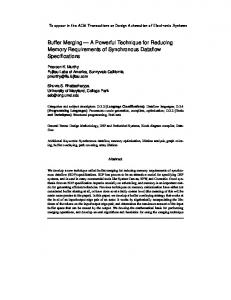
Input Image Row-wise FFT
Columnwise FFT
Output Image Single Input Port
Functional block diagram of 2D-FFT computation.
N row-wise and N column-wise 1D-FFTs, as shown in Fig. 1. Typically, 2D-FFT computation is performed on large images, which require external memory for their storage. Thus, the performance of the 2D-FFT is limited by the bandwidth of external memory, and the FFT computation must be designed carefully to achieve parallelism in conjunction with efficient communication with memory. Previous work has emphasized accelerating 2D-FFT computation by employing multiple 1D-FFT cores. In our approach, we build on this general multiple-core approach, and to make the approach more efficient, we incorporate our recentlydeveloped methods to realize data parallelism within each of the instantiated 1D-FFT cores [1]. We do this by allocating multiple processing units to an individual 1D-FFT core, and incorporating a novel memory addressing scheme. A distinguishing aspect of this approach is that our realization of data parallelism inside a single 1D-FFT core requires only a single pair of vector reading and writing requests to the external memory, regardless of the speed-up factor. Our architecture therefore prevents conflicts among requests from multiple cores in 2D-FFT implementation, and enables better utilization of memory bandwidth. Furthermore, by regularizing the access patterns to external memory, our approach reduces controller complexity and improves predictability. III. 2D-FFT D ESIGN As described above, our approach for ILUT-based acceleration of the 1D-FFT, along with a formal development of the associated addressing scheme, are developed in [1]. In this section, we summarize important features of the ILUTbased approach that are relevant when applying it to 2DFFT implementation, and we present details of the 2D-FFT architecture that we have developed by building on our ILUTbased 1D-FFT accelerator. Henceforth, for conciseness, we refer to our ILUT approach simply as ILUT — that is, by ILUT, we mean our specific approach for FFT inner loop unrolling, as developed in [1], as opposed to the general concept of unrolling inner loops. A. Inner Loop Unrolling Technique (ILUT) (1D) FFT computation involves log N FFT stages, where each FFT stage consists of N/2 butterfly computations. In ILUT, we refer to each FFT stage as an inner loop that “rolls” the butterflies. Also, we roll iterations across FFT stages through a conceptual outer loop. Intuitively, ILUT involves unrolling a given FFT stage by running multiple butterfly operations in parallel. Fig. 2 shows an architectural block diagram of an FFT core after applying ILUT. We parameterize the core with a configurable number B of butterfly units, and increase the value of B to trade-off increased area
1-D FFT Core with ILUT
AGU
Single Output Port
Fig. 2.
N/k
Data Memory Bank0
N/k
Data Memory Bank 1
N/k
Data Memory Bank (k-1)
Interconnection network
Fig. 1.
External Memory
Butterfly Unit 0 Butterfly Unit 1
Butterfly Unit (k-1)
Functional block diagram of ILUT-based, 1D-FFT implementation.
for improved throughput. Addresses for input/output and for the butterfly units are controlled by the address generation unit (AGU). The AGU in our design allows conflict-free, simultaneous read and write accesses to the same dual-ported data memory bank. With this carefully-designed addressing scheme, the size of an individual data memory bank can be reduced by a factor of k when unrolling the inner loop by k (i.e., when k = B). Thus, since k data memory banks are required for an unrolling factor of k, the application of ILUT results in no net change in the overall data memory requirement, regardless of the unrolling factor. In contrast to ILUT, the outer loop unrolling technique (OLUT) allocates multiple FFT cores to achieve parallelism in FFT implementation. OLUT-based approaches have been explored extensively in previous research efforts, such as [8], [7]. Fig. 3 illustrates a functional block diagram of OLUTbased FFT implementation. For an unrolling factor of k, OLUT generally requires a factor of k in memory space increase compared to a single core implementation with no outer loop unrolling applied. Furthermore, OLUT introduces k identical copies of the underlying AGU, so it also involves an increase in the number of FPGA slices required. B. 2D-FFT Architecture Fig. 4 shows a functional block diagram of our proposed 2D-FFT architecture, which we refer to as the IBTF (ILUTBased Two-dimensional FFT) architecture. The IBTF deploys a single 1D-FFT core with ILUT applied within the 1D core to achieve the desired level of parallelism. The 1D-FFT core employed has a single input port and a single output port, regardless of the degree of inner loop unrolling applied to the 1D core. Each of these ports is connected to a dualport memory, which we call the local memory (LM). The LM is used to buffer data between the external memory and the ILUT-based 1D-FFT core. More specifically, the LM is used for sending and receiving vectors of FFT outputs and inputs, respectively, through an external memory interface that operates concurrently with the transform computation within the 1D-FFT core. The LM is divided into two separate regions
Authorized licensed use limited to: University of Maryland College Park. Downloaded on February 26,2010 at 14:21:42 EST from IEEE Xplore. Restrictions apply.
1-D FFT Core with OLUT AGU Multi-Input Ports
N
Data Memory Bank
N
Data Memory Bank
1-D FFT core with ILUT
Butterfly Unit 1-D FFT Core 1
AGU Multi-Output Ports
2-D FFT Core (FPGA Design)
1-D FFT Core 0
CU
Butterfly Unit
N
Fig. 3.
Local Memory For Read (LMR )
External Memory
Fig. 4. AGU
Local Memory For Write(LM W )
Functional block diagram of 2D-FFT with ILUT.
1-D FFT Core (k-1)
Data Memory Bank
Butterfly Unit
Functional block diagram of 1D-FFT with OLUT
— the LMR provides a buffer for reading from external memory, and similarly, the LMW provides a buffer for writing to external memory. Both the LMR and LMW have the same size Sbuffer (in bytes). The LM is implemented on the targeted FPGA device. In general, it can be implemented in FPGA block ram (BRAM) or in FPGA slices (distributed memory). For small to moderate LM sizes, BRAM implementation has the disadvantage that the BRAMs used for the LM are largely underutilized. In our experiments, we have used distributed memory to implement the LM. Such an approach frees up the BRAMs to support other applications or subsystems that co-exist with the IBTF core on the same FPGA device. The control unit (CU) handles the scheduling of all requests for transferring data between the LM buffers and the external memory. Since external memory is volatile, the CU must also take steps to ensure that the data stored in the external memory remains valid throughout its required lifetime. Furthermore, to increase the efficiency of data transfers, the CU accesses external memory through groups of sequential addresses, which are further clustered together in terms of common types of accesses (read or write). This kind of clustered, sequential access pattern is more efficient than more irregular types of patterns (e.g., see [8]). For every iteration of the underlying 1D-FFT transformation, the CU issues Sbuffer read requests followed by Sbuffer write requests. In contrast to ILUT, OLUT-based approaches require k pairs of I/O ports in the external memory interface, along with k 1DFFT cores. Furthermore, the external memory interface in the OLUT approach requires a complex interconnection network, including a crossbar switch, to connect the k pairs of I/O ports, and provide the required external memory access from the set of parallel FFT cores. Furthermore, since the CU must control multiple memory requests from multiple pairs of I/O ports, it needs to incorporate complex scheduling logic to man-
age contention among multiple requests. Hence, OLUT-based implementations of the 2D-FFT can be expected to consume more FPGA slices compared to ILUT-based implementations under the same unrolling factor. We will provide a more indepth comparison on these points in Section IV. IV. A NALYSIS AND C OMPARISON ILUT- BASED AND OLUT- BASED I MPLEMENTATION As described previously, when external memory is involved, the achievable speed-up for a 2D-FFT implementation depends heavily on the bandwidth available for external memory accesses. The on-board external memory on the NI-FlexRio platform provides a bandwidth of 320 MB/s under a 40MHz base clock. Since the default size of data in the interface to the memory is 64 bits, the bandwidth can be viewed as a single sample per a cycle. In both OLUT- and ILUT-based approaches, the CU needs to provide N samples in LMR for the next 1D-FFT computation, and write out N samples from LMW to external memory. Here, N represents the input image size — i.e., the input image contains N xN pixels. During the k-th 1D-FFT computation, the CU must transfer N inputs for the (k + 1)-th 1D-FFT computation in LMR from the external memory. In the same computation frame, the CU also needs to transfer N outputs (produced by the (k − 1)th 1D-FFT computation) from LMW to the external memory. In other words, 2N cycles of data communication are required between the local memory (LM) and the external memory for each 1D-FFT computation, and this is a limiting factor in the achievable throughput. A. Operation of ILUT-based 2D-FFT Implementation A timing diagram for an iteration of ILUT-based 2D-FFT computation is shown in Fig. 5. The data loading and unloading processes can be overlapped in the proposed 1D-FFT IP, and with such overlapping, N clock cycles are required to process N samples. FFT computation follows the loading/unloading process, and for this computation, N/2 · log N cycles are required if no unrolling is applied in the underlying radix-2 1D-FFT. If we apply ILUT with unrolling factor k, then k butterfly units are deployed inside the 1D-FFT core so that the execution time for each 1D-FFT computation can
Authorized licensed use limited to: University of Maryland College Park. Downloaded on February 26,2010 at 14:21:42 EST from IEEE Xplore. Restrictions apply.
be decreased by a factor of k. Therefore, the total time, as a function of the unrolling factor, for 1D-FFT computation is Tinner (k) = N +
N/2 · log N . k
One iteration of FFT computation Load/ Unload
Transformation Process
N cycles
N/2*log(N) cycles
(2)
Now recall that it requires 2N cycles of data communication to prepare the next 1D-FFT computation after the previous 1DFFT computation has completed. Thus, an upper bound on the M AX achieved speed-up can be expressed as Sinner = log N/2. Up to this level of speedup, ILUT exhibits speed-up that is linear to the unrolling factor k. The achieved speedup saturates, M AX however, at Sinner due to bandwidth limitations in the target platform. Note that this analysis is based on our use of 2N cycles as a bound for the required LM-external-memory data transfer between FFT computations. This transfer rate bound is applicable, for example, in the NI FlexRio target platform that we have targeted in our experiments. This bound is also applicable in the OLUT- and external-memory-based 2D-FFT implementations explored in [8]. Changes in this bound, however, require corresponding changes to the speedup analysis presented in this section. ILUT-based implementation promotes efficient utilization of FPGA resources. To see this, recall that LMR (LMW ) connects the input (output) port of the underlying 1D-FFT core to the output (input) channel of the external memory. Because of the regular access patters to and from LM, LMR and LMW can be implemented by FIFO buffers that operate based on standard (push and pop) FIFO access operations, and simple interfacing logic. More specifically, data transfers involving the LM can be controlled by a simple rule — data is pushed or popped as needed whenever the FIFO status is neither “full” nor “empty.” This simplicity is facilitated by the form of data parallelism provided by the ILUT architecture, which is implemented entirely in the 1D-FFT core, and does not require parallel or random-access interfaces to LM. Exploiting this feature allows for resource-efficient implementation of LM and its associated interfaces in distributed memory or BRAM, and allows also for simple, resource-efficient implementation of the CU. B. Operation of OLUT-based 2D-FFT Implementation In OLUT-based FFT implementation, k ≥ 1 FFT cores operate simultaneously, and each of these cores contains a single butterfly unit. Therefore, OLUT enables a reduction in 1D-FFT processing time by a factor of k. To run k 1D-FFT cores in parallel, the associated memory access controller must periodically fill up input data and clear out output data local memory at a sufficient rate. Since 2N cycles are needed for the data transfers associated with each 1D-FFT core, the controller can set up a single 1D-FFT computation frame for each of k 1D-FFT cores every k · 2N cycles. Thus, if Tbase represents the time for 1D-FFT computation without acceleration (k = 1), then we can write
Load Input vector N cycles
Unload Output vector N cycles
One iteration of transferring a pair of input/output vectors with the external memory
Fig. 5.
A timing diagram of ILUT-based FFT computation.
max(Tbase , k · 2N ) k N + N/2 · log N = max( , 2N ). (3) k As with the ILUT-based architecture, the throughput improvement with OLUT is limited by the bandwidth between the FPGA device and external memory. Note also that the minimum inner loop unrolling factor kinner (for ILUT) that is required to reach a given level of throughput is generally larger than the minimum outer loop unrolling factor kouter required to achieve the same level of performance. This is because the total size of the required data memory space (the storage space represented by the blocks labeled as “Data Memory” banks in Fig. 3) for OLUT is kouter times larger than the data memory space required by ILUT, and hence, the net time required for loading and unloading local memory is reduced by a factor of kouter by the ILUT approach compared to OLUT. Note that ILUT requires constant data memory size (independent of the inner loop unrolling factor), and therefore, the net time required by ILUT for loading and unloading local memory is also constant. Overall, even though the larger unrolling factors required by ILUT (for given levels of performance) result in correspondingly higher factors of FPGA resource usage increase due to parallel resource instantiation, this increase is more than compensated by the improvement in the storage requirements of the data memory banks (especially for larger unrolling factors). Thus, when FPGA distributed memory is used to implement local memory, ILUT exhibits a significantly better ratio of achieved throughput to consumed resources (FPGA slices) compared to the OLUT approach. This is demonstrated quantitatively in section V through our experiments. Furthermore, OLUT requires a relatively complex interconnection network to switch paths from multiple I/O ports of the 1D-FFT cores to the local memory subsystem. To maintain peak performance, this interconnection network must be capable of supplying an input vector before each transform computation and receiving an output vector after each computation. Due to the reduced regularity of the memory accesses across the OLUT interconnection network, the loTouter (k)
=
Authorized licensed use limited to: University of Maryland College Park. Downloaded on February 26,2010 at 14:21:42 EST from IEEE Xplore. Restrictions apply.
cal memory cannot be managed in the form of a simple FIFO, as can be done with our ILUT-based architecture. In OLUT, the local memory controller must keep track of the associated row/column vector set for each 1D-FFT transform computation, and must continuously perform book-keeping to switch the interconnection paths. Also, the OLUT controller must perform inter-core synchronization across the set of 1D-FFT cores. As we demonstrate in the next section, the increased control complexity in OLUT results in significant FPGA resource consumption increase compared to ILUT. V. E XPERIMENTAL R ESULTS AND D ISCUSSIONS In our experiments, 2D-FFT designs have been implemented and evaluated for two different sizes of images — 256x256 and 2048x2048. Since a 2048x2048 image requires approximately 33MB of memory, and our targeted platform has 128MB of external memory, 2048x2048 is the largest standard image size (i.e., the number of rows and columns is a power of two) that can be supported on our platform — the next largest image size, 4096x4096 requires approximately 4 × 33MB, which slightly exceeds the available 128MB. We have implemented both inner loop (ILUT) and outer loop (OLUT) unrolling separately in alternative 2D-FFT implementations, and we have carefully compared the results. Each unrolling technique has been applied with increasing unrolling factors until the maximal throughput allowed by the external memory bandwidth was achieved. While the given FPGA target allows us to transfer data between the external memory and FPGA device at a clock frequency of 100MHz, our 2D-FFT implementation cannot operate on such a fast clock. Thus, multiple clock domains are required to support the highest possible memory bandwidth. In this paper, we focus on exploring 2D-FFT design trade-offs for conventional, single-clock-domain implementation, and therefore, we slow the memory interface down to the same speed as the 2D-FFT computation subsystem. More specifically, we use a single clock domain that operates at 40MHz. Applying heterogeneous clock domains to explore further performance enhancement is a useful direction for further investigation. In our OLUT implementation, we employed the LabVIEW FPGA 1D-FFT library module, which is a widely-used commercial 1D-FFT library module that has competitive performance compared to related commercial FPGA cores [1]. In both the OLUT and ILUT implementations, we employed distributed memory to implement the local memory subsystems, as described earlier in Section III. For this purpose, we used the distributed memory library from Xilinx LogiCore [9]. Another useful direction for follow-on research is the integration of block RAM (BRAM) into the design space for optimized ILUT-based 2D-FFT implementation. For our experiments with ILUT, we have restricted the inner loop unrolling factor to be a power of 2 for efficiency in hardware utilization. When ILUT is applied with unrolling factors that are not powers of two, significant resource usage inefficiency results. This is because the 1D-FFT data memory indices cannot be generated simply by concatenating the
binary bit patterns of the memory addresses to that of the associated memory bank addresses, and thus significant overhead results in the address generation logic. While multiple butterfly units jointly compute a single input vector and are controlled by a novel memory address scheme in ILUT, each butterfly unit handles its own individual input vectors separately in OLUT. In this sense, the unrolling factor in OLUT can be a natural number rather than a power of two as in the ILUT case. We compare the proposed ILUT to OLUT under the performance levels that ILUT provides. This comparison may not be a comprehensive comparison between two techniques, but it clearly demonstrates the advantages of ILUT in terms of resource utilization across all of its allowed performance levels. Given a 2D-FFT implementation based on the assumptions described above (a single clock domain and distributedmemory-based local memory), we define the relative resource utilization as the quotient R/T , where R denotes the total number of FPGA slices (including resources for computation and for distributed memory) required for the implementation, and T denotes the throughput in 2D-FFT computations per second. Thus, decreasing levels of relative resource utilization indicate increasing levels of cost-efficiency relative to the achieved processing performance (or conversely, increasing levels of performance-efficiency relative to the achieved cost). Fig. 6 shows the computation time and the number of occupied FPGA slices for 2D-FFT implementation under both ILUT- and OLUT-based approaches with an image size of 256x256. Corresponding values of relative resource utilization are given in Table I. From Fig. 6, we see that OLUT exhibits a smaller computation time compared to ILUT under for an unrolling factor of 2 (k = 2). This is due to the reduced time for local memory loading and unloading, which we discussed in Section IV. Even though there is a difference in throughput for k = 2, both ILUT and OLUT techniques exhibit similar levels of relative resource utilization in Table I. OLUT achieves the maximal achievable throughput (as constrained by the external memory bandwidth) at an unrolling factor of 3, while ILUT achieves the maximal achievable throughput at an unrolling factor of 4. At this maximal performance level, ILUT exhibits 20% less relative resource utilization compared to OLUT, as shown in Table I. This demonstrates the significant resource-efficiency advantage offered by our ILUTbased approach compared to the more conventional approach of OLUT-based 2D-FFT implementation. Computation time and FPGA slice usage results for an image size of 2048x2048 are shown in Fig. 7. While OLUT has a smaller execution time than ILUT with a small unrolling factor, ILUT consistently exhibits better relative resource utilization than OLUT under similar levels of performance. For example, even though ILUT at k = 4 and OLUT at k = 3 employ different unrolling factors, both of these configurations exhibit similar levels of performance, as shown in Fig 7, and these configurations can be compared in terms of the relative resource utilization metric. This is shown in Table II. Furthermore, ILUT consumes a smaller number of FPGA
Authorized licensed use limited to: University of Maryland College Park. Downloaded on February 26,2010 at 14:21:42 EST from IEEE Xplore. Restrictions apply.
12 10 8 6 4 1
2 3 Unrolling Factor
4
5
2700 2400 2100 0
1
2 3 Unrolling Factor
4
5
Computation time and FPGA resource utilization for 2D-FFT with an image size of 256x256.
6000
5200
OLUT ILUT
occupied FPGA slices
Fig. 6.
OLUT ILUT
3000
1800 0
computation time(ms)
3300
OLUT ILUT
16 14
occupied FPGA slices
computation time(ms)
18
5000 4000 3000 2000
OLUT ILUT
4800 4400 4000 3600 3200 2800
0
Fig. 7.
1
2
3 4 5 6 7 Unrolling Factor
8
9
0
1
2
3 4 5 6 7 Unrolling Factor
8
9
Computation time and FPGA resource utilization for 2D-FFT with an image size of 2048x2048.
slices at the highest performance level. The lowest unrolling factor at which OLUT achieves maximal throughput is kouter = 4. However, OLUT cannot be synthesized on our target platform at this unrolling factor. This is because, as indicated by the results from our synthesis attempts, the number of FPGA slices required at this unrolling factor exceeds the number of available slices in the FPGA device. In Table II, we make a note of the “compile error” in the OLUT value at k = 4 to describe that we could not synthesize this case due to limited FPGA resources on the target platform. Even though we cannot synthesize this case, we can estimate its relative resource utilization. Since this case reaches the maximal achievable throughput, it will have the same throughput as the ILUT case with k = 8, as shown in Fig 7. Also, this OLUT configuration (k = 4) is expected to consume more FPGA resources than the OLUT configuration with k = 3 due to increases in the butterfly unit and its associated control logic. In Fig 7, the ILUT configuration with k = 8 shows much better resource utilization than OLUT with k = 3. Hence, we can expect that the ILUT approach has smaller relative resource utilization compared to OLUT when we compare their respective maximal-performance configurations. Another interesting result from our experiments is that the relative resource utilization of ILUT at kinner = 4 is smaller than that at kinner = 8. This is because the potential speed-up at kinner = 8 is not fully realized due to the limited external memory bandwidth. This saturation of performance can be seen in Fig. 7. VI. C ONCLUSION In this paper, we have developed a systematic approach for generating dedicated 2D-FFT subsystems for FPGA implementation. Our approach realizes data parallelism within
TABLE I R ELATIVE RESOURCE REQUIREMENTS FOR AN IMAGE SIZE OF 256 X 256. Unrolling Factor k k k k
=1 =2 =3 =4
ILUT
OLUT
32.96 21.71 N/A 16.18
32.96 21.43 19.36 N/A
TABLE II R ELATIVE RESOURCE REQUIREMENTS FOR AN IMAGE SIZE OF 2048 X 2048. Unrolling Factor k k k k k
=1 =2 =3 =4 =8
ILUT
OLUT
3994 2391 N/A 1632 1736
3994 2546 2244 Compile Error N/A
an individual 1D-FFT core, and minimizes the interface complexity between the underlying 1D-FFT core and local memory. Our approach allows for scalable, parallel 2D-FFT implementation with a relatively simple interconnection network, and correspondingly simple control logic. These features contribute to improved FPGA resource consumption at a given level of performance compared to previous 2D-FFT FPGA architectures. Our methods are demonstrated through extensive synthesis experiments using the Xilinx Virtex-5 FPGA device. Our synthesis results quantify the cost-performance trade-offs provided by our proposed class of FFT architectures. A distinguishing characteristic of our approach, compared to previous techniques for 2D-FFT implementation, is that we provide a
systematic method to generate streamlined, FPGA-based, 2DFFT architectures while taking into account trade-offs between performance and cost. R EFERENCES [1] H. Kee, N. Petersen, J. Kornerup, and S. S. Bhattacharyya, “Systematic generation of FPGA-based FFT implementations,” in Proceedings of the International Conference on Acoustics, Speech, and Signal Processing, Las Vegas, Nevada, March 2008, pp. 1413–1416. [2] J. M. Blackledge, Digital Image Processing. Horwood Publishing, 2005. [3] J. W. Cooley and J. W. Tukey, “An algorithm for the machine calculation of complex Fourier series,” Mathematics of Computation, vol. 19, no. 90, pp. 297–301, April 1965. [4] Y. Ma, “An effective memory addressing scheme for fft processors,” Signal Processing, IEEE Transactions on, vol. 47, no. 3, pp. 907–911, Mar 1999. [5] J. H. Takala, T. S. Ja”rvinen, P. V. Salmela, and D. A. Akopian, “Multiport interconnection networks for radix-r algorithms,” in In Proc. IEEE Intl. Conf. Acoustics, Speech, Signal Processing, 2001, pp. 1177–1180. [6] G. Nordin, P. A. Milder, J. C. Hoe, and M. P¨uschel, “Automatic generation of customized discrete fourier transform ips,” in DAC ’05: Proceedings of the 42nd annual conference on Design automation. New York, NY, USA: ACM, 2005, pp. 471–474. [7] H. Jung and S. Ha, “Hardware synthesis from coarse-grained dataflow specification for fast hw/sw cosynthesis,” in In Proceedings of Int. Conf. on Hardware/Software Codesign and System Synthesis (CODES/ISSS, 2004, pp. 24–29. [8] I. Uzun, A. Amira, and A. Bouridane, “Fpga implementations of fast fourier transforms for real-time signal and image processing,” Vision, Image and Signal Processing, IEE Proceedings -, vol. 152, no. 3, pp. 283–296, June 2005. [9] Xilinx, “Xilinx core generator 10.1,” 2008.
Authorized licensed use limited to: University of Maryland College Park. Downloaded on February 26,2010 at 14:21:42 EST from IEEE Xplore. Restrictions apply.