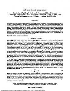
http://www.matweb.com/. [5] Cliff Fung, Rowe Harris, and Terry Zhu, the Foxboro. Co., âMultifunction Polysilicon Pressure Sensors for. Process Controlâ, Sensors ...
Simulation and Modeling of Micro Pressure Sensor Array Jiandong Jin and Zhiping Zhou Microelectronics Research Center Georgia Institute of Technology 791 Atlanta Dr., Atlanta, GA 30332-0269 Fax: 404-894-5172, e-mail: jjin @atlas mirc.gatech.edu
ABSTRACT In order to integrate MEM devices with CMOS circuits, compatibility of materials, micron scale mechanical structures, and the fabrication technology with CMOS is imperative. This paper describes the design of a micron scale pressure sensor array with multi-range and multi-function using ANSYS 5.7. The polysilicon sensor array rests atop multi-layer diaphragms. The specific configuration, the dynamic range, and the performance of individual sensors and the array as a whole are simulated. The resulting sensor array will be integrated with CMOS circuits. Keywords: Pressure sensor array, ANSYS 5.7, CMOS, MEMS, simulation 1. INTRODUCTION Pressure sensors fabricated through MEMS technology are mechanically similar to traditional sensors, with the exception that they are in micrometer scale. The micro scale devices have the additional benefits of small sizes, low inertia and volume, fast response, batch fabrication, and compatibility with the CMOS process (allowing for integration with CMOS circuits). The sensitive resistors of piezoresistive pressure transducers usually rest atop elastic diaphragm. The stress change in the diaphragm causes the resistance change of the pressure sensitive resistor. So, it is very important to calculate the relationship between the stress distribution in the elastic diaphragm and the applied pressure. To increase sensitivity, higher stress is needed on the elastic diaphragm; the highest stress should be much less than the ultimate strength of the material. This includes consideration of the combined effect of piezoresistive coefficient and stress, with regard to the design of resistors. Stress calculation by use of the Finite Element Method has been reported by Yicai Sun [1]. ANSYS has been widely used in industry for simulating the mechanical, thermal, and electrical properties of MEMS structures. It can also be used to simulate the relationship between the mechanical parameters of the pressure sensor and the particular device structures and material parameters. To our knowledge, it has not been used in simulation of the micro pressure sensor array. In this paper, ANSYS 5.7 is used to simulate the stress and strain distributions of particular
the simulation results, the most optimized areas to place sensor resistors, elastic diaphragm shape, sensor measurement ranges, and sensor cavity depths are determined.
2. DESIGN AND SIMULATION 2.1 The outline of the sensor chip The distribution of stress on elastic diaphragm depends on the diaphragm structure and material properties. Each chip includes one temperature sensor, three absolute pressure sensors, one differential pressure sensor, and one signal collecting and processing circuit. One of the absolute pressure sensors has the same diaphragm size as the differential pressure sensor. All the sensitive resistors are doped polysilicon. The size of the sensors varies from tens microns to hundreds of microns; the minimum line width is two microns. Beneath the diaphragm are vacuum cavities and hole ports. When pressure is applied to the sensor array, the diaphragms deform, causing resistance changes that are processed by the circuit on the other side. The layout of the sensor array is shown in Fig. 1. However, the resistors on the diaphragms are not drawn to scale.
CMOSCIRCUIT
AP3
AP1
DP
AP2
Fig.1. The sensor array layout Patterns AP1, AP2 and AP3 are the diaphragms of the absolute pressure sensors. Pattern DP is the diaphragm of the differential pressure sensor. The other two green blocks are the places of the temperature sensor resistors. The middle line is the site for lead pads. The half area above is circuit part. All sensors are rectangular in shape and doped l ili i d ii i l Th l f
line width is two microns. The pressure sensitive resistors are resting atop the elastic diaphragm, consisting of a dual layer of polysilicon and Si3N4, each one-micron thick [5]. When pressure is applied to the sensor, the diaphragms deform, and the resistance changes proportionally. In the resistor pattern design, aluminum is used instead of polysilicon at the parts parallel with the y-axis. The cross sections of the structures of differential and absolute pressure sensors are shown in Figs. 2 and 3.
main steps in procedure 1. Different values of pressure can be applied onto the top of the diaphragm by resuming the saved data through ANSYS menu function after meshing.
2.2.4 Sensor array simulation Procedure 3 was repeated to simulate the different diaphragms with piezoresistors. The stress and strain distributions and the maximum deformation simulation results were obtained under different pressure.
3 ANALYSIS Fig.2. The cross-section of a differential pressure sensor
Fig.3. The cross-section of an absolute pressure sensor
2.2 Simulation
2.2.1 Elastic diaphragm modeling Menu and Program File were used to draw the analysis model. The diaphragm model input was written in Notepad and read into ANSYS. The model input includes the diaphragm shape, size, location and material properties. After the diaphragm model displays on the screen, common pre-processor menus are used to define the simulation parameters.
When analyzing a set of similar models, it is more flexible to create the model by editing program files rather than by working through menus. It is much easier to change the model geometry and physical parameters in the program files. In design, modeling from an edited program can save design time. However, when simulating pressure conducting stress distribution and diaphragm deformation, use of the menu control is more convenient. The file can be saved as “*.db” file after meshing. Different pressures can then be applied by using the resume command from the saved file. The rectangular diaphragm consists of two layers: One layer is polysilicon, and the other is silicon nitride. The resistors are made of polysilicon and aluminum, so there are three different materials in all. All volumes should be defined with respective material parameters. In ANSYS, it is important to use a consistent system of units for all the data. For MEMS, it is important to choose convenient units, since components may be only a few microns in size. This paper uses the conversion factors from standard MKS to µMKSV. To make sure the simulation results are accurate, proper element type should be selected. The mesh size should be set as small as possible. The calculation time will increase as the mesh size decreasing. Table 1 shows the useful parameters of the three materials in the simulation.
2.2.2 Diaphragm size The diaphragm model size or the ratio of length to width was changed in the Notepad and save as another file name. Repeat the procedure 1, different size models can be simulated.
Table 1. Material Properties Poisson’s Ratio
Aluminum[2]
Young’s Modulus (Mpa) 72000
Polysilicon[3]
169000
0.22
Silicon Nitride[4]
158000
0.26
Material properties
0.33
2.2.3 Diaphragm with sensor resistors analysis From procedures 1 and 2 the proper diaphragm shape is selected. Add the pressure sensor resistor model on the selected elastic diaphragm model through the saved Notepad file. Since part of the resistor will use aluminum, the physical parameters of a third material should be
Yield Strength (Mpa) 275.8 1200 (tensile) strength) 172 (tensile strength)
Simulation procedures 1 and 2 obtain the stress and strain distribution plots, comparing the maximum (tensile)
diaphragms are simulated. Thus, certain rectangular diaphragms with large strain or stress ratio can be selected in further simulation. The distributions reveal the positions on the diaphragms that the absolute stress is high. In order to optimize placement of sensor resistors, the polysilicon parts of the resistors are along X direction. Simulation procedures 3 and 4 allow simulation of the stress distribution and diaphragm deformation on the three different-sized pressure sensors. At the point where the maximum (tensile) stress approaches the yield strength, the applied pressure value is the upper limit of the sensor measurement range for a given diaphragm. The maximum deformation value can be used to select a cavity depth. The bottom of the cavity is designed to protect the diaphragm from fracture due to over-range pressure.
the polysilicon resistors that rest on the longer sides of the diaphragm.
Fig.4. Strain distribution on 56µm×84µm diaphragm, applied pressure is 100psi.
4 ANALYSIS RESULTS AND DISCUSSION 4.1 Finding the optimal areas for placement sensor resistors The rectangular distribution simulation on the rectangular diaphragm indicates that under a given pressure, the maximum stress or strain is found at the middle of the longer sides. The minimum stress or strain (compressive) is in the center of the rectangular itself. To obtain the maximum output of sensors, sensitive resistors should be placed on the areas where the strain is large. Furthermore, the strain values on the edges and in the center are opposite. Thus, when pressure increases, the resistance of the resistors on the edges of the longer side also increases, while the resistance of the resistors in the center decreases.
4.2 Selecting elastic diaphragm shape From the simulation result in Table 2, and considering the sensor array arrangement, rectangular diaphragm is selected. The higher the ratio of length vs. width, the higher the ratio of maximum (or minimum) strain (X direction to Y direction), the smaller the influence caused by transverse gauge factor. A rectangular diaphragm with length to width ratio of 1.5 is selected to apply in the further simulation step. The SM represents of maximum stress value, and the SMN means the minimum stress value. Letters X and Y stand for the direction.
Fig.5. Stress distribution on 56µm×84µm diaphragm, applied pressure is 100psi
4.3 Pressure sensor measurement range simulation
Figs 6 and 7 show the simulation results of the relationship between pressure and the maximum stress, and the relationship between pressure and the maximum deformation. The diaphragm size is 64µm×84µm. The yield strength of polysilicon is 1.2±0.15Gpa. When the applied pressure causes the maximum stress on polysilicon to reach the yield strength, the pressure value is the upper limit of the sensor measurement range.
Table 2. Diaphragm shape simulation result compare Length/ width SMX/S MY SMNX/ SMNY
1:1
1.5:1
2:1
3:1
1
1.54
1.92
2.30
1
1.48
1.45
1.38
Figs 4 and 5 show the simulation plots with piezoresistors on the top of the diaphragm. The diaphragm size is 56
Fig.6. Simulation of the relationship between pressure and maximum stress
5
Fig.7. Simulation of the relationship between pressure and maximum deformation of the diaphragm
4.4 Over-range protection Beneath the pressure diaphragm is a cavity. The bottom of the cavity supports the deformed diaphragm. When pressure is applied on the diaphragm, the diaphragm will deform. If the diaphragm deformation is large enough to touch the bottom of the cavity, the bottom will support the diaphragm and will protect the diaphragm from fracture. Under full range pressure, the maximum diaphragm deformation determines the depth of the cavity. The simulation results are shown in Table 3. Table 3. Pressure measurement limit simulation Diaphragm size
25_m× 37.5_m
37.5_m ×56_m
56_m×84_ m
Applied pressure (Kpa) Max. deformation (_m) SMX(X direction max. strain)
6890
3450
689
0.060
0.097
0.114
0.0072
0.0051
0.0156
SMN(X direction min. strain) SMX(X direction max. stress) (KPa) SMN(X direction min. stress) (KPa)
-0.0030
-0.0017
-0.0087
1240
890.676
1036
-442.766
-238.503
-272.414
Experiments will be run to test the simulation results, especially the ultimate strength of each diaphragm. And the influence of residual stress in materials will be included [6].
CONCLUSION
The simulation discussed above gives the following conclusions. ANSYS 5.7 software has been successfully used to simulate strain and stress on one-micron polysilicon and one-micron silicon nitride thin films. A complete simulation model for pressure sensor arrays has been established. Using the model, a variety of pressure sensors array with different measurement ranges, different diaphragm sizes, diaphragm thickness, and cavity depths can be easily designed. The pressure sensors in the array are in micron scale. The materials used are the same as those used in CMOS circuits, and its fabrication process is compatible with IC technology. Therefore, the pressure sensor array can be integrated with CMOS circuits.
REFERENCES [1] Yicai Sun, Yuling Liu, and Qinghao Meng, “Design, Fabrication and Application of Pressure Sensor”, Beijing, Metallurgy Industry Publisher, 2000. [2] "Material properties" http://wotan.me.unm.edu/tran/Mat-Props.html. [3] William N. Sharpe, Jr., bin Yuan, and Ranji Vaidyanathan, “Measurements of Young’s Modulus, Poisson’s Ratio, and Tensile Strength of Polysilicon”, Proceedings of the Tenth IEEE International Workshop on Microelectromechanical Systems, Nagoya, Japan, PP 404429,1997. [4] “The online material information resource”, http://www.matweb.com/ [5] Cliff Fung, Rowe Harris, and Terry Zhu, the Foxboro Co., “Multifunction Polysilicon Pressure Sensors for Process Control”, Sensors, Oct. 19, 1997. [6] Tai-Ran Hsu and Nansheng Sun, "Residual Stresses/Strains Analysis of MEMS," Technical Proceedings of MSM, Santa Clara, pp. 82-87, 1998.