Robust Design of Third Level Packaging in Portable Electronics: Solder Joint Reliability under Dynamic Mechanical Loading Sridhar Canumalla Texas Instruments, 12500 TI Boulevard, MS 8640, Dallas, TX 75243
[email protected] Abstract Solder joint reliability issues that can be identified only at the system level are notoriously difficult to resolve in a timely manner using trial and error experimentation alone. The particular case of solder joint reliability of a side switch in a phone subjected to drop-impact is addressed. An approach employing Response Surface Methodology (RSM) is proposed to solve reliability and robust design problems in advanced packaging. In particular, a 10x improvement in the drop test failure rate is demonstrated with a minimum of trial and error experimentation. Technical contributions are a) a novel drop life response function derived from strain energy principles, and b) an approach to address package reliability issues at the system level. Nomenclature The different variables in the model are: r maximum extension of the rod under dynamic δ max loading s extension of the spring under dynamic loading δ max EA is the constant of the rod with Young’s modulus L E, cross sectional area A and length L spring constant of the spring ks Mg δ sts = s is extension of the spring under static loading k Mg is extension of the rod under static loading r δ st = r k ∆ε P the plastic strain range experienced during fatigue loading PK k = E PK A PK LPK is the stiffness coefficient for the power key k PS = µ PS (1 − AVoid )A PS h PS is the stiffness coefficient for kr =
the power switch AVoid is the void fraction in the solder joint Introduction Portable electronic products, such as mobile phones, music players, and personal digital assistants have become ubiquitous. They not only serve as extensions of our persona but also as fashion accessories. Consequently, along with ease of use, the appearance and industrial design of these handheld electronic products is a key care-about for customers. One way to achieve this balance is to incorporate dedicated controls for functions such as speaker volume, camera shutter release, ON/OFF, etc. via the use of side switches. Mounting side switches along the narrower sides of the portable product makes it possible to devote the front face of the device to the
978-1-4244-2231-9/08/$25.00 ©2008 IEEE
user interface and other attractive design elements such as logo, key pad, etc. Another benefit of using dedicated side switches is that it allows for one handed operation of those controls. The placement of the side switches along the narrower sides of a phone would not have reliability implications if it weren’t for the relatively harsh mechanical loads encountered in the use environment. Phones and other handheld, portable electronic products are subjected to severe mechanical loads when dropped onto a hard surface from heights ranging from 0.5 m to 1.5 m [1]. These drop-impact events are somewhat random in real life with regard to the magnitude of the loads and orientation of the impact. Product failure under drop-impact loads can involve display failures, housing cracks, fracture of the solder joints under chip scale packages (CSPs) mounted on the printed wiring board, etc. In recent years, a large body of literature has been devoted to understanding the mechanics of solder joint fracture for CSPs and other area array components such as land grid array (LGA) packages (see [1] for references). Industry standards are also used to help the original equipment manufacturers (OEMs) assess the susceptibility of their products to failure under drop-impact loading [2]. However, applicability is limited only to 2nd-level packaging (board level) and not to 3rd-level packaging (system level). There is a dearth of published data on system level reliability under drop-impact loading because of the complexity of the loading and specific solutions cannot be generalized over a broad range of product shapes, sizes and construction. One consequence is that the system level product designers and reliability engineers can only resort to costly experimentation, where the outcome is at best an empirical understanding that cannot be generalized to subsequent products. As a result, components whose reliability can only be assessed at the system level, such as the tactile power switch (or side switch), can present high field failure risk. Retooling the product design to address these issues is not preferred because 3rd level packaging failures often come to light very late in the product development process. The goal here is to demonstrate an approach to achieve robust design of the power key + side switch + solder joint subsystem using a more rigorous approach rather than depending solely on empirical testing. The direct benefits of such an approach are rapid and effective resolution of failures with a minimum of trial and error experimentation. Estimating Reliability as a function of different process, design and material variables - Response Surface Methodology (RSM), is a collection of statistical techniques that can be used for developing and optimizing products or processes. A number of monographs are available on the subject, for example, by Myers and Montgomery [3]. RSM is
1187 2008 Electronic Components and Technology Conference
particularly suited in situations where several independent input variables influence the response. Often, the response function is nonlinear with local minima and maxima. Assuming that the response function is linear can lead to incorrect optimization. In practice, the true response function is often unknown, and the experimenter has to resort to a series of controlled experiments and use statistical modeling to develop an empirical approximation of the underlying response. In the current approach, however, a theoretical response function is derived relying on the mechanics of dynamic deformation rather than designed experiments. The applications of RSM can be categorized as a) mapping the response surface over a particular region or operating conditions, b) optimization of the response, and c) selection of independent variable values to achieve specific response values. The approach in this paper falls under the last category and demonstrates how design and material variables can be chosen to meet specific drop test requirements. Robust Design - A “robust” product is one that is insensitive to factors that are difficult to control. The methodology for robust design was introduced and popularized by Taguchi [4]. The RSM approach offers a collection of statistical analysis tools to adopt Taguchi’s robust design concept more efficiently. Accordingly, noise variables are also included in the response function. The statistical analysis in this study was carried out using commercial statistical analysis software [5]. Power Key
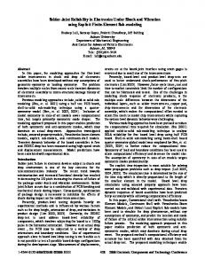
Experimental The portable electronic products under test (mobile phones), were characterized using a Phoenix 160 PCBA Xray machine, a Mettler Toledo analytical balance, standard sample preparation equipment, a Nikon ME6000P Eclipse metallurgical microscope and a LEO1450VP electron microscope. The electron microscope was used primarily in the back scattered detection mode to highlight the compositional contrast in the polished and fracture surfaces. A proprietary product level drop-impact testing machine was used to conduct drop tests on the phones. The composition of the solder used to mount the side switch to the PWB was Sn3.5Ag0.7Cu. Results and Discussion Reliability Testing & Failure Analysis The tactile switch, which is soldered down onto the printed wiring board (PWB), typically consists of two or more leads that can take gull wing or straight down configurations. A metal can is attached to these leads and this houses the switch activation mechanism that is engaged by pushing a plunger (Figure 1). This plunger is in close proximity to the edge of the PWB after phone assembly, and located adjacent to the power key that is usually made of an elastomeric material. The power key engages the plunger and activates the power switch. An X-ray picture of the power switch soldered on the PWB reveals the voids that are often encountered in practice, and must be considered a “noise” variable (Figure 2).
Plunger
Side Switch Soldered Leads Figure 1. Photograph of power key adjacent to a side switch soldered on a PWB. Figure 3. Back-scattered SEM picture of the side-switch lead.
Figure 2. X-ray micrograph of the power switch solder joints illustrating the void content in the joint.
The initial reliability results were obtained by conducting repeated free fall testing on 15 phones, and each phone was dropped 24 times from a height of 1 m on to a concrete surface. Six of the phones failed in these initial reliability tests. In other words, the failure rate was 40% with the initial design. The upper and lower 95% confidence bounds on the failure rate are 64.25% and 19.8%, respectively. Extensive voiding was found on the fracture surfaces as well as in the prepared cross-sections (Figures 3 – 5). The void fraction measured from X-ray radiographs using image analysis was found to vary from 0.1 to 0.3. The solder joint often fractured along the component IMC layer as seen in Figures 4 and 5. In addition, some samples
1188 2008 Electronic Components and Technology Conference
showed concomitant damage under the pad (Figure 4). The IMC morphology (Figure 5b) did not possess any abnormalities to indicate that either the surface mount process was suboptimal or material incompatibilities [5] were limiting the strength of the solder joint. There was little evidence that the solder joint deformed plastically during the drop test. These microstructural observations are used to formulate the appropriate assumptions for deriving the drop life response function.
Figure 4. Backscattered SEM picture of a partially broken side switch solder joint showing the presence of multiple damage modes: IMC fracture at component interface and pad peeling.
a
b Figure 5. a) Metallurgical micrograph of a broken side switch solder joint showing the intermetallic compound (IMC) morphology b) Higher magnification metallurgical micrograph of the boxed region reveal the scallop-shaped IMC morphology.
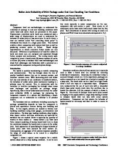
Dynamic Loading and Model Development When the phone is dropped on the power key, the force exerted on the power key is transmitted to the power switch and thereafter to the solder joints anchoring the power switch to the printed wiring board (PWB) (Figure 6a). Conceptually, dropping the phone containing the power key + power switch + solder joint subassembly such that it lands on the power key is analogous to dropping a collar of mass M onto a spring as shown in Figure 6b. Using this analogy, the power key is equivalent to the spring and the solder joints are collectively equivalent to the rod. The strain in the solder joints can be estimated by solving for the deformation of the rod in the reduced dynamic loading model. The key concept in dynamic loading is that the stresses and strains induced by suddenly applying a load (dynamic loading) are much higher than by gradually applying the same load (quasi-static loading) [6]. For example, depressing the power key to activate the switch exerts a quasi-static load while dropping the phone on the power key exerts a dynamic load. A fish bone diagram of the different input variables is shown in Figure 7. The variables not included in the model are a) effect of surface finish (component and PWB pad), b) paste printing quality, and c) reflow profile. The variation in the different variables is summarized in Table 1. The “Distribution(Parameter1, Parameter2) refers to the distribution used for describing the variables. For a Normal distribution, the parameters represent the mean and standard deviation, respectively. For a Uniform distribution, the parameters represent the lower and upper limits, respectively. Unless otherwise specified, a standard deviation of 10% of the mean value is used. The development of the model involved the following simplifying assumptions: 1) The bulk properties of lead free solder can be expected to be significantly different from the solder joints properties because of the abundance of intermetallic phases. Since the constitutive behavior for the solder joints is unknown, the relatively well known bulk, elastic properties are used instead of non-linear properties of questionable validity. As a result, the life predicted by the model can be expected to be approximate and conservative. 2) The criterion for passing the drop test is arbitrarily fixed at 24 drops. 3) The spring inside the power switch, which toggles the activation of the switch, has a very low stiffness. The energy expended in deforming this spring is neglected. 4) The deformation inside the solder joint is uniform elastic shear. This is a simplistic assumption. 5) The strain calculated ( γ solder ) is assumed to be the total strain (elastic + plastic), and is used in the CoffinManson equation to calculate the drop life without partitioning the plastic strain range ( ∆ε P ). The impact of this approximation is an overly conservative estimate of the drop life. 6) Even though failure analysis data indicate minimal plastic deformation and localized fracture process in
1189 2008 Electronic Components and Technology Conference
Design Variables Length of Power Key Diameter of Power Key contacting Power Switch
System Factors
Force required for activating Power Switch
Stress imposed in test (drop height)
Area of Solder Joint
Mass of Portable Product
Height of Solder Joint
Drop Reliability Solder Material
Reflow Profile
PWB pad finish
Paste Printing Quality
Component surface finish Modulus of Power Key
Etc. Void Fraction in Solder Joint
Modulus of Solder Material
Process
Fatigue Coefficient and exponent
Materials
Figure 7. The fish bone (Ishikawa) diagram of the different variables that could affect the drop life in reliability tests. the proximity of the component IMC layer, the entire solder joint participates in absorbing the energy due to the drop-impact. Response Function for Drop Life Dynamic loads are fundamentally different from static loads in terms of the response. A static load is applied gradually, increasing from zero to the maximum value, while a dynamic load is applied very suddenly. The almost instantaneous application of the load gives rise to stress waves, vibrations and other nonlinear effects. Examples of dynamic loading include impact loading, jumping onto a pogo stick or dropping a mass onto a spring. The outcome of the rather complex deformation behavior is that the deflections produced are significantly higher than if the load is applied in a static or quasi-static fashion. Complete analysis of the system behavior and estimation of the drop life for the case when the phone is dropped on the power key is not a trivial exercise, and requires the use of expensive and time consuming finite element analysis coupled with experimental validation. Nevertheless, an approximate analysis can be achieved by using the concept of strain energy and by making some simplifying assumptions. In the rod and collar shown in Figure 6b, the potential energy of the collar (mass M), in relation to the spring, is converted into kinetic energy as the collar falls. At the instant the collar strikes the flange-spring, the potential energy transforms into kinetic energy which is given by Mv 2 2 , where v is the velocity of the falling collar. This kinetic energy is divided into the strain energy of stretched rod, strain energy of spring, partly dissipated as heat and partly as the kinetic energy of the collar, which either continues to move downward or bounces upward. The collar is assumed to stick to the flange and move downward along with the compressing spring. In other words, perfectly plastic impact is assumed. The model is based on the assumption that all the potential energy is converted into elastic strain energy of deformation. Energy losses due to heat, etc. are disregarded. Any change in the potential energy of the rod itself is ignored as is the residual
kinetic energy of the collar after impact. It is assumed that the stresses in the bar remain in the linear elastic range and the stress distribution for the dynamic case is the same as for the static case. Examining the rod and collar case (Figure 6b), the potential energy (PE) of falling mass M is given by the equation r s (1) PE = Mg (h + δ max + δ max ) The second term inside the parenthesis in (1) represents the deformation of the rod due to dynamic loading and is higher than the static deformation due to mass M. Similarly, the third term represents the dynamic deformation for the spring. From a simple force balance, the extension in the spring and rod are related to their spring constants by the relationship kr r s r (2) δ max = s δ max = k *δ max k The sum of the strain energies (U) stored in the spring and rod are given by the following equation
)
(
2
(
)
2
r s k r δ max k s δ max (3) + 2 2 Mechanistically, the drop life optimization can be interpreted as partitioning the total energy between the spring (power key) and the rod (solder joint) to achieve optimal deformation in the rod (solder joint). For the case of a phone, the equivalent stiffnesses are k s = k PK and k r = k PS . Equating the potential energy with the strain energy stored in the assembly, we get the following quadratic equation
U=
(
)
(
)
r k r δ max 2
2
2
+
(
s k s δ max 2
(
)
2 r s = Mg (h + δ max + δ max )
(4)
)
2
r r k r δ max k s k *δ max r r + = Mg (h + δ max + k *δ max ) (5) 2 2 Solving the quadratic equation r s r r (6) (δ max )2 ⎡⎢ k2 + (k * )2 k2 ⎤⎥ − δ max Mg + k * Mg − Mgh = 0 ⎦ ⎣
[
]
and substituting k r = k PS and k s = k PK , we get
1190 2008 Electronic Components and Technology Conference
δ PS =
[(
)
2
(
( ) )]
M g (1 + k * ) + M g (1 + k * ) + 2M g h k PS + k PK k *
( )
k PS + k PK k
* 2
2
1
2
(7) The shear strain in the solder joint can be calculated as δ PS (8) γ solder = PS h Since the drop test is in essence a high strain rate, low cycle fatigue process, the Coffin-Manson relationship is used to calculate the drop life to predict the life is given as (9) (N f )α ∆ε P = θ
solder joint quality of other components in the phone. Changes in the solder material and the mass of the phone involved severe constraints in both time and cost. Solder joint height changes, while relatively inexpensive, would have required changes to the paste printing stencil thickness and SMT process, which would involve lengthy lead times. Most importantly, one variable with relatively small cost and time constraints was identified: power key material.
Power Switch
Power Key
Where α = 0.89, is the fatigue ductility exponent and 0.63 ≤ θ ≤ 0.85 is the fatigue ductility coefficient for Sn-rich
solders [7, 8]. Table 1. The input variables used in the calculation of drop life. The symbol “◊” refers to experimentally measured values. Variable Dist (Param1, Param2) units Normal (2e-3, 1e-4) m Length of Power Key ◊ Dia. of Power Key 5 10-4 m contact area ◊ Normal (8.45·10-7, 2·10-8) m2 Area of Solder Joint ◊ Normal (50·10-6, 2·10-6) m Height of Solder Joint ◊ Void Fraction in Solder Uniform (0.1 , 0.3) Joint ◊ Modulus of Power Key Normal (2.5·109, 2.5·108) Pa Fatigue Coefficient 0.7 Fatigue Exponent -0.89 Solder Shear Modulus 25·109 Pa Normal (83·10-3, 83·10-5) kg Portable Product Mass ◊
PWB
Plunger
Table 2. Constraints on the variables affecting the drop life. Variable Cost Time Solder joint area Low High Solder material High High Solder joint height Medium Medium Power key material Low Low properties Power key dimensions Low Medium Void Fraction Low Medium Mass of Phone High High Response Surface Methodology Budgetary and time constraints are important considerations in any optimization exercise, and these constraints are listed in Table 2. For example, the solder joint area could be changed with little expense but using a side switch with larger lead area would have involved time penalties because the new part would have to be qualified across several products. A second variable, void fraction in the solder joint, was found to be inexpensive to optimize, but would have required lengthy lead times to optimize the surface mount reflow profile without negatively impacting the
Figure 6. a) Schematic of the power key + side switch + solder joint sub-assembly b) reduced dynamic loading model where the spring, collar and rod are analogous to the power key, phone mass and solder joint, respectively The calculated nominal life of the phone using the values (shown in Figure 8) was 27 drops. Monte Carlo simulation with 104 trials indicated that the failure rate was 100%. In comparison, the experimental drop test failure rate was about 40% with lower and upper 95% confidence bounds on the
1191 2008 Electronic Components and Technology Conference
failure rate at 19.8% and 64.25%, respectively. The response function estimates are significantly higher than the experimentally measured failure rate. A sensitivity analysis of the response function indicated that the drop life was sensitive to power key modulus much more than other variables (Figure 9). Since the sensitivity of the response (drop life) to the modulus of power key was significantly higher than for other variables, optimization was first conducted on this variable. Drop life response optimization was carried out by allowing changes only to the power key modulus (shown by the unchecked box in the Lock column), and all other variables were constrained. The lower limit for the power key modulus was fixed at 1 MPa and the upper limit at 10 GPa based on the material choices available to the design team. Optimization calculations converged to a power key modulus of 5 MPa with an associated nominal drop life of approximately 857 drops, which is approximately 30 times higher than the initial drop life (Figure 10). Current X Lock
Factor Mass of Phone A_ps A_void mu_solder h_PS E_PK d_PK L_PK h fatigue_coeff alpha
Response
0.083 8.475e-7 0.2 2.5e+10 0.00005 2.5e+9 0.0005 0.002 1 0.7 -0.89
Lo Limit
Hi Limit
0.008 8.0722e-7 0.1016939 2.5e+10 0.000035 1000000 0.0004014 0.0015416 0.5055479 0.625 -0.9
0.1055637 8.9665e-7 0.2932831 2.5e+10 0.00012 1e+10 0.0005926 0.0024979 1.4959715 0.85 0.2
Current Y
Lo Limit
26.936725
.
Drop Life
Hi Limit Benchmark .
26.936725
Figure 8. Simulation of the drop life with initial conditions. The variation in the optimized response function was examined by varying each variable while holding the others constant, and the results are shown in Figure 11. Again, it is seen that the most sensitive variable is the modulus of the power key, although the sensitivity to diameter of the power key was elevated slightly compared to initial simulations. Tactical feel is a response requirement that needs to be considered when changing the modulus of the power key. In practice, the modulus of the power key cannot be reduced ad infinitum to improve drop life because the tactile response is
degraded. In this case, the tactile response with the 5 MPa modulus power key materials was sufficient to warrant further reliability testing on phones with the more compliant power key material. When choosing a particular optimized solution, it is also important to ensure that the slope of the response function in the immediate vicinity is sufficiently flat to make it robust against natural variation. A contour plot of the variation of drop life as function of the modulus of power key and mass of phone is plotted in Figure 12. For a product mass of 0.083kg and a power key modulus of 5 MPa, the drop life is relatively robust to small changes in the mass and the drop life does exceeds 650 drops even towards the edge of the plot area. The same information can be represented as a surface plot (Figure 13), where the nominal values are indicated by vertical planes. The intersection of the planes is found to lie relatively far away from the regions where the response surface is very steep, indicating that the selected modulus value contributes to a relatively robust design. Intuitively, void fraction in the side switch solder joint may appear to be one of the first variables to control to improve drop life. However, the response surface in Figure 14 suggests that the drop life is relatively insensitive to void fraction as compared to the modulus of the power key for a wide range of power key moduli. The use environment of portable electronic products involves drop-impacts from various heights ranging from 0.5 m to 1.5m, where the lower drop would be representative of the user dropping the phone from the waist level and the higher drop representative of a user dropping the phone while holding the phone to the ear and standing at the same time. Therefore, the response surface is discussed in terms of the height of drop and modulus of power key. The plot in Figure 15 of this response surface shows that the response function is relatively flat in the vicinity of the design value selected for the power key modulus (5 MPa). This indicates the design is robust over phone drop heights ranging from 0.5 to 1.5m. The response function is found to be a nonlinear function of both the power key modulus and the drop height (Figure 16). Experimental Validation of Reliability Improvement The power key material with modulus of 5 MPa was selected based on the response surface methodology described
Drop Life 26.93672
500 400 300 200 100
8.475e-7 A_ps
0.2 A_void
0.00005 h_PS
2.5e+9 E_PK
0.0005 d_PK
1.8e-3 2e-3 2.2e-3 2.4e-3
5.5e-4 6e-4 1.5e-3
5e-4
4e+7 6e+7 8e+7 1e+8 4e-4 4.5e-4
1e+7
1.1e-4
9e-5
0.25 0.3 7e-5
0.2
0.15
8.3e-7 8.5e-7 8.7e-7 8.9e-7 0.1
8e-7
0
0.002 L_PK
Figure 9. Sensitivity profile plots for A PS , void fraction, h PS , E PK , d PK and LPK .
1192 2008 Electronic Components and Technology Conference
earlier in this paper. To validate the model, 26 phones were dropped from a height of 1m for a total of 24 drop-impacts each. Only one phone failed due to the solder joint shearing off the PWB. Weibull plots were also constructed by using Monte Carlo simulation with the variables listed in Table 1. The initial drop life was estimated by using the experimentally measured variation shown in Table 1 with a power key modulus of 2.5 GPa, while the improved drop life data was estimated by using a power key modulus of 5 MPa for 100 test cases. In both cases, a Normal distribution was used with a standard deviation of 1% of the mean value. A 2-parameter Weibull plot comparing the initial and improved life estimation is shown in Figure 17. The characteristic life (η) and the shape parameter (β) estimates are listed in Table 3. Although an improvement in the drop life of approximately a factor of 30 was predicted by changing the modulus of the power key, the experimentally observed improvement is relatively more modest and the nominal failure rate was reduced from an initial value of 40% to less than 5%. Convergence Convergence Limit Criterion
Objective Trips Max Cycles Max Iter 857.08029077
20
50
500
0.00000001
0.000101883
Maximize
Current X Lock
Factor Mass of Phone A_ps A_void mu_solder h_PS E_PK d_PK L_PK h fatigue_coeff alpha
Response Drop Life
0.083 8.475e-7 0.2 2.5e+10 0.00005 5000000 0.0005 0.002 1 0.7 -0.89
Lo Limit
Hi Limit
0.008 8.0722e-7 0.1016939 2.5e+10 0.000035 1000000 0.0004014 0.0015416 0.5055479 0.625 -0.9
0.1055637 8.9665e-7 0.2932831 2.5e+10 0.00012 1e+10 0.0005926 0.0024979 1.4959715 0.85 0.2
Current Y
Lo Limit
857.08029
.
Hi Limit Benchmark .
26.936725
Figure 10. Simulation of the drop life with optimized conditions. The optimization was carried out only on the modulus of the power key. The improvement in drop life was obtained by reducing the strain imposed on the solder joint. The plot in Figure 18
shows the relative change in the solder strain predicted by the model and the corresponding improvement in drop life. The predicted strain values suggest that the improvement in drop life was achieved by reducing the strain in the solder joint of the power switch. Table 3. Weibull parameters for the initial and improved drop life estimations using the response function. Condition Estimate Lower Upper 95% 95% 882.57 868.01 896.93 Improved η Improved β 12.77 10.94 14.74 Initial 28.42 27.96 28.87 η Initial β 13.163 11.23 15.24 Conclusions Solder joint reliability of the side switch has been improved using a theoretically derived response function for the drop life. RSM and Monte Carlo simulation were used to understand the response surface for several variables. Based on sensitivity analysis, the modulus of the power key was changed from an initial value of 2.5 GPa to 5 MPa, which improved the drop test failure rate from 40% to less than 5%. The strain energy based mechanics model proposed in this paper also has broader applicability for addressing other kinds of drop-impact driven reliability issues and would require some modifications to the derived response function. The approach discussed demonstrates how design changes based on response functions and stochastic simulation can improve package reliability in a timely and cost effective manner with a minimum of trial and error. For package development programs that are perennially under severe time and cost constraints, this approach can help improve quality and reliability while including the effect of inevitable variations in packaging materials and processes in mass production. The areas of applicability include warpage control of stacked packages, thermomechanical reliability of solder joints, etc. Even if the response function cannot be obtained in closed form, response surface DOE methods can be employed to estimate the response function. Once the response function is estimated, RSM can be used to arrive at material, design or process variables to improve the reliability with a minimum of trial and error.
Drop Life 857.0803
2500 2000 1500 1000 500
8.475e-7 A_ps
0.2 A_void
0.00005 h_PS
5000000 E_PK
0.0005 d_PK
1.8e-3 2e-3 2.2e-3 2.4e-3
5.5e-4 6e-4 1.5e-3
5e-4
4.5e-4
1e+7 4e-4
7.5e+6
5e+6
2.5e+6
1.1e-4
9e-5
0.25 0.3 7e-5
0.2
0.15
8.3e-7 8.5e-7 8.7e-7 8.9e-7 0.1
8e-7
0
0.002 L_PK
Figure 11. Profiler plot of sensitivity of the drop life with the improved power key material.
1193 2008 Electronic Components and Technology Conference
1050 850 1250 1450
1e+7
David Buraczyk is appreciated. I am grateful to Dr. J. Venkataramana for helpful discussions on the model.
650
9e+6
References
8e+6
1.
E_PK
7e+6 6e+6 5e+6 4e+6
2.
3e+6 2e+6
3.
1e+6 0.01
0.03
0.05 0.07 Mass of Phone
0.09
4.
Figure 12. Contour plot of drop life as a function of power key modulus and the mass of the phone.
5. 6.
7. 8.
9. Figure 13. Surface plot of the drop life as a function of the power key modulus and mass of the phone.
S. Canumalla, and P. Viswanadham, 2007, “Interconnect Reliability Considerations in Portable Consumer Electronic Products,” in Micro- and Opto-Electronic Materials and Structures: Physics, Mechanics, Design, Reliability, Packaging, eds. E. Suhir, Y.C.Lee, and C.P.Wong, Springer, New York, pp. 251-298. JESD22-B111, Board Level Drop Test Method of Components for Handheld Electronic Products, JEDEC Solid State Technology Association, 2003. Myers, R.H., and Montgomery, D.C., 2002, Response Surface Methodology: Process and Product Optimization Using Designed Experiments, Wiley. Taguchi, G., 1986, System of Experimental Design: Engineering Methods to Optimize Quality and Minimize Cost, UNIPUB, White Plains, NY. JMP ™ v7, SAS Institute, NC, USA. S.K.Saha, S. Mathew, and S. Canumalla, 2003, “Effect of intermetallic phases on performance in a mechanical drop environment: 96.5Sn3.5Ag solder on Cu and Ni/Au pad finishes ”, Proc of 2004 Electronic Components and Technologies Conference (ECTC), May 28-30, 2003, Las Vegas, LA, pp. 105-112. J.M. Gere and S. Timoshenko, Mechanics of Materials, 1990. C. Kanchanomai, Y. Miyashita, Y. Mutoh, S.L. Mannan, “Influence of frequency on low cycle fatigue behavior of Pb-free solder 96.5Sn/3.5Ag,” Materials Science and Engineering A, vol. 345 (2003), pp. 90-98. C. Kanchanomai, Y. Miyashita, Y. Mutoh, “ Low cycle fatigue behavior and mechanisms of a eutectic Sn–Pb solder 63Sn/37Pb,” International Journal of Fatigue, vol. 24 (2002) pp. 671–683.
Figure 14. Surface plot of the drop life as a function of the power key modulus and void fraction in the solder. Acknowledgments The help of Sesil Mathew and Murali Hanabe in sample preparation and microscopy, and Al Griffin’s feedback on manuscript are appreciated. The management support of
Figure 15. Surface plot of the estimated drop life as a function of the power key modulus and drop height.
1194 2008 Electronic Components and Technology Conference
Drop Life 857.0803
1500
1
1250
0.5 0.3
1000 750
0.1
500
Strain
250
5000000 E_PK
1.5
1.25
1
0.75
1e+7 0.5
8e+6
6e+6
4e+6
2e+6
0
1 h
0.03
0.01 0.006 0.004
Figure 16. Plot of the drop life as a function of the a) power key modulus and b) height of drop with the finally selected power key material.
0.002
Improved
0.001 0.0006
1
Improved Initial 0.95 0.8 Weibull Cumulative
Initial
0.06
2 3 5
10 20 40 100 Drop Life
1000
Figure 18. The improvement in drop life was obtained by reducing the strain imposed on the solder joint. The plot shows the relative change in the solder strain predicted by the model and the corresponding improvement in drop life.
0.5 0.2 0.1 0.05 0.02 0.01 10
20 30
50
100 200 Drop Life
500
1000
Figure 17. Probability plot of predicted life with initial and improved power key material. Estimated cumulative failures are 16% and 0%, respectively.
1195 2008 Electronic Components and Technology Conference