2.2 Manual tuning principles with multiple optical ring resonators . . . . . 11 .... times T and the extra phase shifts Ï1, Ï2 and Ï3 due to the heater on top of the ring.
University of Twente Department of Electrical Engineering Chair for Telecommunication Engineering
Staggered delay tuning algorithms for ring resonators in optical beam forming networks by R.J. Blokpoel
Master thesis Executed from December 2006 to August 2007 Supervisor: Prof. Dr. Ir. W. van Etten Advisors: Dr. Ir. C.G.H. Roeloffzen Dr. Ir. A. Meijerink Ir. L. Zhuang
Summary The Telecommunication Engineering group at the University of Twente is currently working on two projects about phased array antenna systems with photonic beamformers. One is the SMart Antenna systems for Radio Transceivers (SMART) project. The other is the Broadband Photonic Beamformer project. Some of the advantages of implementing the beam forming network in the optical domain are immunity to electromagnetic interference, high bandwidth and low loss. The optical delays needed for the beamforming are realized with Optical Ring Resonators (ORRs), which can be tuned by varying their parameters. To get higher delay values multiple rings are cascaded and the rings should be tuned in such a way that the delay ripple is minimal in the frequency band of interest. The goal of the assignment was to design a subsystem which converts a desired set of delay values into a set of optimal ORR parameters. The first step to do this was to derive optimality criteria. Three different criteria were the result of this: the delay criterion, phase criterion and power criterion. All of them used a metric value which was the sum of the squared deviation from the target at a certain number of points. Three tuning algorithms followed from those criteria by optimizing for the criteria using Non Linear Programming (NLP) techniques. The phase tuning algorithm was concluded to be best suited to use for the derivation of rules of thumb. This was because negative side effects of improper tuning like the rise of side lobes in the radiation pattern are directly dependent on the phase error and the power tuning algorithm gave only slightly better results at the cost of a significant increase in complexity. Since these algorithms were too complex to implement directly into a microcontroller, rules of thumb were needed. One option was a lookup table, which had severe memory requirements since the 2 kB for a 1×4 OBFN was approaching the limits of the current system. The other option was to store only coefficients of curve-fitted polynomials, which saves a lot of memory at the cost of a little processing time and accuracy. The research also gave solutions for adapting the algorithms when a different ORR response formula is found or when the system needs to be expanded to a 1×M OBFN. Another result from the research was the delay tuning range covered by a certain number of rings. From that the conclusion was drawn that only three rings were needed in the first stage of a 1×8 OBFN instead of four. iii
Contents Summary
iii
1 Introduction 1.1 Background . . . 1.2 Framework . . . 1.3 Assignment goal 1.4 Organization . .
. . . .
1 1 5 5 6
2 Properties of the optical ring resonators 2.1 Structure of a single optical ring resonators . . . . . . . . . . . . . . . . 2.2 Manual tuning principles with multiple optical ring resonators . . . . . 2.3 Crosstalk between different heaters . . . . . . . . . . . . . . . . . . . .
7 7 11 12
3 Effects of optical beam forming network parameter errors 3.1 Delay ripple and phase errors . . . . . . . . . . . . . . . 3.2 Imperfections in the optical beam forming network chip . 3.3 Derivation of optimality criteria . . . . . . . . . . . . . . 3.3.1 Delay criterion . . . . . . . . . . . . . . . . . . . 3.3.2 Phase criterion . . . . . . . . . . . . . . . . . . . 3.3.3 Power criterion . . . . . . . . . . . . . . . . . . .
. . . . . .
15 15 20 21 21 23 23
. . . . . . . . .
27 27 29 29 31 33 35 36 36 38
. . . .
. . . .
. . . .
. . . .
. . . .
. . . .
. . . .
. . . .
. . . .
. . . .
. . . .
. . . .
. . . .
. . . .
4 The Optimal Tuning Algorithms 4.1 Optimization Method . . . . . . . . . . . . 4.2 Results for delay response tuning . . . . . 4.2.1 One ring . . . . . . . . . . . . . . . 4.2.2 Two rings . . . . . . . . . . . . . . 4.2.3 Three rings . . . . . . . . . . . . . 4.2.4 Tuning a 1×4 optical beam forming 4.3 Results for phase response tuning . . . . . 4.3.1 Method used for phase tuning . . . 4.3.2 One ring . . . . . . . . . . . . . . . v
. . . .
. . . .
. . . .
. . . .
. . . .
. . . .
. . . .
. . . .
. . . .
. . . . . .
. . . . . . . . . . . . . . . . . . . . . . . . . . . . . . . . . . . . . . . . . . . . . network chip at . . . . . . . . . . . . . . . . . . . . . . . . . . .
. . . .
. . . . . .
. . . .
. . . . . .
. . . .
. . . . . .
. . . . . . . . . . . . . . . once . . . . . . . . .
. . . .
. . . . . .
. . . . . . . . .
. . . .
. . . . . .
. . . . . . . . .
. . . .
. . . . . .
. . . . . . . . .
. . . . .
39 41 41 42 43
5 Derivation of rules of thumb 5.1 One ring . . . . . . . . . . . . . . . . . . . . . . . . . . . . . . . . . . . 5.2 Two and three rings . . . . . . . . . . . . . . . . . . . . . . . . . . . . 5.3 Comparison between lookup table and fitted polynomials . . . . . . . .
47 47 50 54
6 Practical aspects of delay tuning methods 6.1 Expansion to 1×M optical beam forming network . . 6.2 Different response formulae . . . . . . . . . . . . . . 6.3 Fabrication offsets and unpredictable parasitic effects 6.4 Number of rings required . . . . . . . . . . . . . . . .
. . . .
57 57 59 59 61
7 Conclusions and Recommendations 7.1 Conclusions . . . . . . . . . . . . . . . . . . . . . . . . . . . . . . . . . 7.2 Recommendations . . . . . . . . . . . . . . . . . . . . . . . . . . . . . .
63 63 64
4.4
4.5
4.3.3 Tuning a 1×4 optical beam forming Results for power tuning . . . . . . . . . . 4.4.1 Method used . . . . . . . . . . . . 4.4.2 Results . . . . . . . . . . . . . . . . Comparison of tuning methods . . . . . .
network chip at . . . . . . . . . . . . . . . . . . . . . . . . . . . . . . . . . . . .
. . . .
. . . .
. . . .
once . . . . . . . . . . . .
. . . .
. . . .
. . . .
. . . . .
. . . .
. . . . .
. . . .
. . . . .
. . . .
Appendix A Description of Non Linear Programming method used
69
B MATLAB scripts and functions B.1 Visualization functions . . . . . . . B.2 Optimization algorithms . . . . . . B.3 Scripts used for the rules of thumb B.4 Script used to generate error curve
71 71 74 84 86
. . . .
. . . .
. . . .
. . . .
. . . .
. . . .
. . . .
. . . .
. . . .
. . . .
. . . .
. . . .
. . . .
. . . .
. . . .
. . . .
. . . .
. . . .
. . . .
. . . .
Chapter 1
Introduction 1.1
Background
The major benefits of phased-array antenna systems are their high gain and possibility of electronic beam steering and shaping, which is together called beam forming. A phased-array antenna system consists of multiple antenna elements with corresponding tunable phase shifters or delay elements, and some splitting/combining circuitry. Delay elements should be used instead of phase shifters when it is applied to broadband beam forming. The steering resolution for the system then depends on the tuning resolution of the delay elements. There are several advantages when the beam forming network is implemented in the optical domain. The system will be immune to electromagnetic interference and will have a high bandwidth and low loss. Also it will be compact and have a low weight when it is implemented using integrated optics. More on various types of optical delay elements can be found in [6]. The complete system is shown schematically in Figure 1.1. AEs
E/O
OBFN
angle
control
O/E
Rx
Figure 1.1: The complete antenna system The first block represents the Antenna Elements (AEs), which are fed to the Electrooptic (E/O) converter, to get the signals into the optical domain. Then the signals from the different AEs are delayed in the Optical Beam Forming Network (OBFN). This is steered by the control block which has the beam angle as input. With this angle the delay values for each AE are calculated so that there is positive interference for radio signals coming from the desired direction at the end of the OBFN. Finally the output of the OBFN is converted back to the electric domain in the O/E block and fed to the 1
2
Chapter 1. Introduction
→ group delay
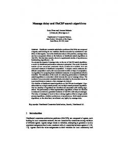
Rx block for detection. PSfrag replacements The OBFN block is very important for the system and will be discussed in more detail. It contains splitters, combiners, Mach-Zehnder interferometers (MZIs) and optical ring resonators (ORRs). Especially the ORRs are interesting, since they cause the required delays for positive interference between signals from different AEs. When a straight optical waveguide is coupled to an ORR, it will behave as an all-pass filter with a periodic bell-shaped group delay response. This is illustrated by the dashed lines in the figure below, which are the individual group delays of the ORRs shown in the inset.
0
f1 f2
f3
φ1
φ2
φ3
in T
T
T out
κ1
κ2
κ3
→f
Figure 1.2: Theoretical group delay response of three cascaded ORR sections (taken from [7]) The resonance frequencies of the ORRs, f1 , f2 and f3 , depend on the round-trip times T and the extra phase shifts φ1 , φ2 and φ3 due to the heater on top of the ring. The group delays at the resonance frequencies depend on the coupling coefficients κ1 , κ2 and κ3 . Both the φs and κs can be tuned using chromium heaters, based on the thermo-optical effect. More details on this can be found in Chapter 2. As can be seen from Figure 1.2 a broadband delay element can be created by cascading multiple ORR sections. The total group delay response (the solid line) simply follows by summing the individual responses (the dotted lines). In this way a flattened response with some ripple on it can be obtained by tuning the ORRs to different resonance frequencies. This is called staggered delay tuning. As can be seen from Figure 1.2 the response of a single ring is much narrower than the cascade of three, so more rings give more bandwidth. When the center frequencies are placed further apart, the bandwidth will be larger but the ripple will also be larger. A solution to keep the ripple at the same level is to use more rings. So more rings means a higher bandwidth or smaller ripple, or a combination of both. However the fabrication costs of the chip increase with the number of rings. Therefore the number of rings is kept minimal. When all the delay elements and splitting/combining circuitry are realized in the optical domain and integrated onto one chip, an optical beam forming network (OBFN)
1.1.
Background
3
is obtained. An example of a 1×4 OBFN, based on a binary tree topology, is shown in Figure 1.3. f3 out 1 k6
in
3
out 2
f1
f2
k3
1
2
f4 out 3
k1
k2
k5 k7
4
out 4
k4
Figure 1.3: 1×4 binary tree OBFN (taken from [1]) This principle was recently demonstrated in [1]. The major advantage of using a binary tree structure is that less rings are required to get four different outputs. Since each output has one ring more in the optical path than the previous one, the delay can be selected in steps. This can be seen in Figure 1.4, where some group delay response measurements of this 1×4 OBFN chip are shown. Output 1 does not have any rings and is therefore not present in the graph. Output 2, 3 and 4 respectively have 1, 2 and 3 rings in their path, which results in a linearly increasing delay, when properly tuned. In [7] the same is done for a 1×8 OBFN chip. 0.6 ~ 1.5 GHz
® group delay (ns)
0.5
output 2 output 3 output 4
0.4 0.3 0.2 0.1 0.0 1549.97 1549.98 1549.99 1550.00 1550.01 1550.02 1550.03 ® wavelength (nm)
Figure 1.4: Output measurements of 1×4 binary tree OBFN (taken from [1]) The heater elements in the OBFN chip were manually tuned such that flat group delay responses over a bandwidth of 1.5 GHz were obtained. As mentioned earlier, the
4
Chapter 1. Introduction
manual heater tuning is a laborious procedure, which becomes increasingly complicated for increasing number of cascaded ORR sections. Obviously manual tuning is not desirable in a phased-array antenna system using optical beam forming. The next block in Figure 1.1 to discuss is the control block. Its main function is to calculate the voltages which should be applied to the heaters of the ORRs. This is not a straightforward operation and therefore it can be divided into several functions. This is shown in Figure 1.5 Transmit/receive angle(s)
Group delays, amplitudes
Optical parameters
Voltages
Figure 1.5: The project layers
The first layer is the transmit or receive angle of the antenna system. This angle is determined from the position of the other end of the communications link. When either end of the link is moving, a tracking system should also be included in this layer. In Figure 1.1 it is shown as input for the control element. When the angle is known, the group delays and amplitudes for the array elements can be calculated. This is done in the second layer, which passes information about delays to the next layer. Here the optical parameters for the ORRs are calculated to get an optimal delay or phase response. The layer should also compensate for additional optical phases due to some problems which are specific for the chosen OBFN structure. More on those problems can be found in Chapter 2 and 3. The last layer calculates and applies the voltages to the heaters of the ORRs using information of the layers above. So using the ORRs described in [1] and [2], the implementation of the layers remain as a problem to complete the system. In [3] a solution to the problem of crosstalk between the heaters is presented. It also considers the problem in the last layer of voltage calculation. A solution to apply the voltages to the heaters is presented in [4]. It makes use of a microprocessor which controls a multichannel DAC chip with an analog amplifier at the output. The distribution of control signals and the voltages is done by means of a bus using IDE connectors. The current and temporal solution for the third layer is manual tuning of the OBFN chip. This is an undesirable activity, which is increasingly complicated with the number of elements in the antenna system and the number of ORRs in the chip.
1.2.
1.2
Framework
5
Framework
This assignment is part of two research projects carried out by the Telecommunication Engineering group at the University of Twente. The aim of these projects is to develop an antenna array system with photonic beamformers. One is the SMart Antenna systems for Radio Transceivers (SMART) project, which should provide mobile wireless broadband communication access. The pilot should be a system suited to place in an aircraft and uses novel broadband (2 GHz) antenna concepts to receive satellite television. The delays should be tunable between 0 and 5 ns. The project is carried out in cooperation with LioniX, National Aerospace Laboratory NLR and Cyner Substrates. The other project is the Broadband Photonic Beamformer project, which is carried out with LioniX and Astron. The application for the phased array is astronomy in this case. The array will be over one squared kilometer and signals should be processed very accurately over a very broad frequency range. So both projects use the same kind of system but have different bandwidths and frequencies and delay values.
1.3
Assignment goal
With such a large aimable antenna array as in the Broadband Photonic Beamformer project or with a moving object like in the SMART project, the tuning cannot be done manually since it would take too much time for the application. Therefore the tuning should be done automatically. A subsystem should convert a desired delay value to a set of φs and κs to pass on to the next layer. As explained before this will belong to the optical parameters conversion function from Figure 1.5. The goal of this assignment is to design such a subsystem for the phased-array antenna system. First an algorithm should be made which just converts the input delay value into the required optical parameters resulting in an optimal delay curve. The algorithm should not have too high memory of processing power requirements. When that is done it should be linked to the next layer and take crosstalk of the heaters into consideration too. When time permits it the assignment could also include a calibration procedure to tackle the problem of fabrication offsets in the ORRs. Another possibility is to go up in the layer structure and look at the problem of a tracking system to keep the array aimed at the other end of the communications link. Which way is chosen depends on the prior results and the total project state at that moment. Of course other ways can come up during the research too.
6
1.4
Chapter 1. Introduction
Organization
A deeper understanding of the working principle of the ORRs is needed to carry out this assignment. Therefore Chapter 2 treats the ORRs in more detail, with formulae for phase and delay responses and the basics of manual tuning. It also contains more details about the crosstalk problem. The next chapter describes the effect of OBFN parameter errors (such as delay ripple) to the performance of the system, resulting in criteria to evaluate tuning algorithms. In Chapter 4 of this report the theoretical algorithm is explained. The next chapter will treat a solution based on a rule of thumb, which is easier to implement and saves a lot calculation time but will be less accurate. Also the alternative of a lookup table will be considered. Finally in Chapter 6 conclusions will be drawn.
Chapter 2
Properties of the optical ring resonators 2.1
Structure of a single optical ring resonators
To be able to solve the problem of tuning the delay elements, it is of course necessary to have a deep understanding of the working of a single ORR. The structure of the ORR is shown in Figure 2.1. In the figure E is the optical field, with E1 the input of the ORR and E2 the output. Two parameters in the structure are tunable: the first one is the coupling constant κ of the coupler and the second is the additional phase φ. The roundtrip time of the ring is T . Using these parameters the group delay response for a single lossless ORR is, according to [1], given by τ (f ) =
κT 2 − κ − 2 1 − κ cos (2πf T + φ) √
(2.1)
In [2] a more accurate formula for this response is presented. This one takes losses in the optical ring into account
τ (f ) =
1 − r2 (1 − κ) T √ · 2 1 + r2 (1 − κ) − 2r 1 − κ cos (2πf T + φ) T r2 − (1 − κ) √ + (2.2) 2 1 − κ + r2 − 2r 1 − κ cos (2πf T + φ)
with r = 10−α/20 and α is the loss of the ring in dBs. More about these losses can be found in Chapter 3. The formulae (2.1) and (2.2) are derived for an ORR with a single fixed coupler, but the one used in this research is a tunable coupler, consisting of two fixed couplers with a phase shifter in between them. To get more insight in the differences between those, the structure of the fixed type is presented schematically in Figure 2.1 and the tunable one in Figure 2.2. 7
8
Chapter 2. Properties of the optical ring resonators
φ
PSfrag replacements
T κ
E3
E4
E1
E2
Figure 2.1: Detailed structure of the fixed ORR with only one directional coupler φ PSfrag replacements
T θ E3 E1
κi
κi
E4 E2
Figure 2.2: Detailed structure of the tunable ORR with two directional couplers. Direct derivation of formulae for the group delay in the tunable structure gives quite large expressions. Therefore it is better to keep working with (2.1) and (2.2) while doing the staggered delay tuning and apply a correction afterwards. This correction can be derived by writing the structure of the tunable ORR in the same way as the old one with some corrections. The relation between the fields at the inputs and outputs in the fixed one is given by # #" # " √ " √ 1−κ j κ E3 E4 √ (2.3) = √ E1 j κ 1−κ E2 The tunable structure consists of two of such couplers and an extra phase shift in the upper branch between those two couplers. It is easy to produce equal values for the κi s of both couplers in the fabrication process and therefore they will be assumed identical.
2.1. Structure of a single optical ring resonators
9
When the extra phase shift is included into the second matrix the following expression is obtained for the new structure "
E4 E2
#
=
#" #" √ #" # √ √ 1 − κi j κi 1 − κi j κi ejθ 0 E3 √ √ √ √ 1 − κi 1 − κi j κi 0 1 j κi E1
" √
(2.4)
When those three matrices are multiplied it results into the transmission matrix (H) of the complete system with the following entries � � H11 = ejθ/2 (1 − κi )ejθ/2 − κi e−jθ/2 i hp p H12 = ejθ/2 j κi (1 − κi )ejθ/2 + j κi (1 − κi )e−jθ/2 i hp p −jθ/2 jθ/2 jθ/2 H21 = e j κi (1 − κi )e + j κi (1 − κi )e � � H22 = ejθ/2 (1 − κi )e−jθ/2 − κi ejθ/2
(2.5)
Note that this matrix could also be obtained by analyzing all possible paths for each matrix entry, which of course gives the same result. The factor ejθ/2 is pulled out of the matrix. This is done to make the rewriting of the entries H12 and H21 (which are equal) easier and is done as follows H12 = H21 = 2jejθ/2
p
κi (1 − κi ) cos (θ/2)
(2.6)
From this the total κ for the ORR (like the κ in Figure 2.1) can be derived which is expressed in κi and θ as κ = 4κi (1 − κi ) cos 2 (θ/2)
(2.7)
Using this definition for κ it can be seen that H12 and H21 can now be written as √ j κejθ/2 , which makes those entries equal to those of (2.3). For the entry of H11 a more advanced trick has to be applied to get to an expression which fits into the original structure. First the Euler formula is applied to get (1 − κi )ejθ/2 − κi e−jθ/2 = (1 − 2κi ) cos (θ/2) + j sin (θ/2)
(2.8)
The next step is to write this in the polar representation: H11 =
p 1 − 4κi (1 − κi ) cos 2 (θ/2) · exp (jΦ + jθ/2)
(2.9)
The square root in the first part of the right hand site of the equation is equal to √ 1 − κ when compared to (2.7). To keep the formulae small and comprehensible an argument Φ is defined by tan Φ =
tan (θ/2) (1 − 2κi )
(2.10)
10
Chapter 2. Properties of the optical ring resonators
The derivation of H22 is analogous to the one of H11 and results into the same modulus but this time with a phase of −Φ + θ/2. Combining these results the transmission matrix H now becomes H=e
jθ/2
"
ejΦ 0 0 1
#" √
# #" √ 1−κ j κ 1 0 √ √ j κ 1−κ 0 e−jΦ
(2.11)
With this result for H, the ORR of Figure 2.2 is expressed with almost the same transmission matrix as in (2.3). The only differences are some phases. With those phases pulled out of the matrix the use of formulae (2.1) and (2.2) is justified again. The phase of ejθ/2 was already out of the matrix and can be seen as two phase shift blocks between the coupler and the outputs E2 and E4 . For the phases Φ and −Φ the matrix of (2.3) should have its upper row multiplied with eΦ and its left column with e−Φ . The same effect can be achieved by adding a phase shift of Φ between the coupler and output E4 and a phase shift of −Φ between input E1 and the coupler. However the input of the ORR is E1 and the output is E2 , so from a system point of view it does not matter whether the shift of −Φ is placed after E1 or before E2 . Using these derivations a new equivalent structure for the one of Figure 2.2 can be made in which the formulae of (2.1) and (2.2) can be used. This structure is presented in Figure 2.3. φ PSfrag replacements
Ψ1 E3
κ E4 Ψ2
E1
E2
Figure 2.3: Detailed structure of the corrections applied to the fixed ORR to be equal to the tunable one. The phase shift Ψ1 is equal to Φ + 2θ and Ψ2 is equal to −Φ + 2θ . When the staggered delay tuning using (2.1) and (2.2) is finished φ can be corrected by subtracting Ψ1 and Ψ2 has to be taken into account when the optical phases in the different ports of the OBFN chip have to be matched. In an ideal ORR, κ can be varied between 0 and 1. However when taking a closer look at (2.7) and the structure of the ORRs in Figure 2.2 (which is used in [2]), it
2.2. Manual tuning principles with multiple optical ring resonators
11
can be seen that the coupling constants, κi s, of the directional couplers determine the maximum value of κ. As mentioned earlier it is not difficult to get equal values for the κi s in the fabrication process, but it is hard to get them exactly at 0.5. As can be seen from (2.7), the maximum value of the total κ is reached when the phase shift θ is 0 degrees, since the cosine term then becomes one, and is given by κmax = 4κi (1 − κi )
(2.12)
The best value for the fabricated κi s currently achieved was 0.465 and using (2.12) this results in 0.9951 as maximum for κ. The minimum value of κ is always zero, since the cosine term is zero when θ is set to π2 .
2.2
Manual tuning principles with multiple optical ring resonators
To get more insight in the tuning procedures it is useful to look at some basic principles of manual tuning. Using this, one can immediately compare the results of the automatic tuning algorithm with it and see whether the algorithm gives meaningful results. In Figure 2.4 an example of manually tuning a 1×4 OBFN chip is given. Note that the axes are both normalized with respect to the roundtrip time T . Tuning the first output (one ring) is quite easy: the phase should be tuned so that the bell-shaped response is exactly in the middle of the tuning bandwidth. The κ should be set to a value which gives a slightly too high delay value in the center of the tuning range and slightly too low on the edges. That way the average error is the smallest. The second output with two ORRs is more difficult. One ring should have its peak delay value a little to the left of the tuning range and the other to the right. That can be seen from the dotted responses which are the two separate rings which together form the second output. That way a response is created which is higher at the edges and lower in the middle. It can be tuned more flat by pulling both responses to the middle, but that would not benefit the last output. Also important is the symmetry for the tuning: both ORRs should have the same κ and should lie at equal distance from the center. The sum of the first and second output gives the last output. Since the first one is always too high in the middle it should be compensated for by the second one to get the last as flat as possible. However the optimalization algorithm should give the answer to what is exactly the best way of tuning. Now the difference in delay between the first and second output is too small in the center and too big at the edges, with a relatively flat response for the third one. One could imagine that there is a certain
12
Chapter 2. Properties of the optical ring resonators
5.5 5
Normalized Group Delay
4.5 4 3.5 3 2.5 2 1.5 1 0.5 0 -0.2
-0.15
-0.1
-0.05 0 0.05 Normalized Frequency
0.1
0.15
0.2
Figure 2.4: Results of manually tuning a 1×4 OBFN chip. The outputs have increasing delay values with the number of rings. The first output is with only one ring (dash-dotted), the second with two rings (dashed) and the last (solid) is the sum of both and thus has the highest delay value. The output with two rings is composed of the two dotted responses. The dashed grid represent the target bandwidth and delay values for the tuning. optimum between tuning the third one flat or tuning the second one flat. This is also where the relations between the different outputs in the chip become important and that is described in Section 3.3.
2.3
Thermal crosstalk between different heaters
The problem of crosstalk between the heater elements on the OBFN chip was already mentioned in the introduction and will be further explained in this section. In [3] the problem for two heaters which should cause certain phase shifts is treated. The relation between phases and voltages is given by: "
φ1 φ2
#
=
"
a b c d
#"
V12 V22
#
(2.13)
in which the φs are the phase shifts, the V 2 s the squared input voltages to the heaters and a, b, c and d are the transfer coefficients between the voltages and phases. So not only V1 determines φ1 , but also V2 as can be seen from the formula. This is due to the
2.3. Thermal crosstalk between different heaters
13
crosstalk between the heaters. The heat from one heater will spread out over the chip and causes some heating in other regions too. When for example the heater on top of Figure 2.2 is turned on, there will be a rise in temperature in the environment of the lower heater too. When a and d are taken 9 and b and c are 1 for example, it results in Figure 2.4, which is taken from [3]. 8
6
4
2
0 0
2
4
6
8
Figure 2.5: Possible values for the phase shifts, φ1 and φ2 , while tuning with crosstalk. The allowed values are in the white area (taken from [3]) As can be seen from the figure it is not possible to have a shift of π at φ1 and 0 at φ2 . The solution to reach those values is to turn on the other heater too such that φ2 will become 2π, which of course has the same effect as 0. In [3] an iterative scheme is presented to calculate the voltages while taking the crosstalk into account. First it determines the value as if there were no problem with negative phase shifts. This is done by inverting the matrix. However some desired values, the ones in the gray areas to the left and below the white parallelogram, will result in negative phase shifts when the matrix is inverted. This is when the iterative part of the scheme comes in since it starts to add 2π to each heater outside the tuning range until a valid solution is reached. That way a solution is reached without negative phase shifts. It can be
14
Chapter 2. Properties of the optical ring resonators
used to any number of heaters. The parallelogram in Figure 2.4 would then become an n-dimensional one, but the principle remains the same.
Chapter 3
Effects of optical beam forming network parameter errors 3.1
Delay ripple and phase errors
The goal of this assignment is to design a subsystem which converts a desired delay value to a set of φs and κs in such a way that an optimal response results. This section describes the effects of errors in the phase response. Using that theory it is possible to evaluate whether the subsystem reaches an optimal solution or not. The delays are required to aim the phased array antenna in a certain direction. So only with correct delays the signals will have optimal constructive interference resulting in the highest output power. To get more insight in the effects of delay or phase errors to the output power, it is good to take a look at the direct effects of delay ripple to the output of a single DE. In Figure 3.1 the group delay response of a DE with much ripple and one with little ripple is presented. Details about those simulations can be found in [9]. It can be clearly seen that the input pulse is severely distorted when the DE has a large ripple. Also the transcient time will be much longer which could be a source for Inter Symbol Interference (ISI). The next step to get the total output power is to take a look at the expression for the desired signal s(t) =
X
rn (t) cos (2πfIF,n t + ψn (t))
(3.1)
n
The set n represents the different subcarriers in the spectrum considered, so fIF,n are the carrier frequencies. The amplitude rn (t) and phase ψn (t) depend on the modulation type of the signal. When all carriers are summed the desired signal results. In fact this can be seen as the input for the system. It is also important to look at the kind of modulation and detection used in the system to get to an expression for the output power. In Figure 3.2 a block diagram of 15
16
Chapter 3. Effects of optical beam forming network parameter errors 50
1.25 1
Light intensity
Normalized group delay
1.5
40
30
20
10
0.75 0.5 0.25
Output Input
0 -0.25 -0.5 0
0 -0.1
0.05 -0.05 0 Normalized frequency (times 2pi)
0.1
25
50
75
100
125
150
175
200
Time (Unit delay)
(a)
(b)
C d
(c)
(d)
Figure 3.1: A group delay response with large ripple (a) and the corresponding pulse response (b) and the same with a small ripple in (c) and (d). For comparison the Desired Output (DO) is plotted in (d) too. (taken from [9])
the system concentrating on the modulation is presented. There is a Single SideBandSupressed Carrier SSB-SC) modulation block for each output signal of an AE, but first each signal is amplified by a Low Noise Amplifier (LNA). The index m represents the different AEs and goes from 1 to M . More details about the SSB-SC block can be found in [16]. Now the basic principle behind the delays in the OBFN is presented. This is the last step toward an expression for the output power. In a phased-array antenna system the desired signal is received in each AE with a certain time delay due to the physical location of the antenna. So each AE will receive s(t) with an additional time delay (T m ). When extra time delays are added in a correct manner all signals from the different AEs will have constructive interference for radio waves coming from a certain direction. These extra time delays are caused by the DEs in the OBFN chip. So s(t) should arrive at the detector for all AEs with a delay of Tmax , which is an arbitrary common delay
3.1. Delay ripple and phase errors
17
AE
PSfrag replacements
LNA E1 (t)
SSB-SC Ein (t)
Eout (t)
AE
OBFN
Iout (t)
LNA EM (t)
SSB-SC
Figure 3.2: OBF system with optical SSB-SC modulation and balanced coherent detection. (taken from [12]) and should be larger than all delay values Tm . To achieve this, the OBFN should add a delay of Tmax − Tm to every signal. In [5] the theory of [8] with formulae for the output power in the ideal case is used together with a few assumptions to get the relation between output power and phase error. So when the magnitude response and group delay response within a particular channel are assumed to be flat, the output field is equal to
1 Eout (t) = 2
r
M Po X X am |Hm (fo + fIF,n )| exp (j∆φm (fo + fIF,n )) 2Ls Lc n m=1
· rn (t − Tmax − ∆τm (fo + fIF,n )) exp (j2πt(fo + fIF,n ))
+ j2π(fIF − fIF,n )Tmax + jψn (t − Tmax − τm (fo + fIF,n )) (3.2)
with Po the optical power, and Ls and Lc the splitting and combining loss, respectively. The index m represents the different AEs, so am is a weighting factor for each different AE to the output, the absolute value of Hm is the magnitude response through the OBFN chip for such a signal. The group delay ripple ∆τ will in general be much smaller than the symbol time, which is 25-50 ns for Digital Video Broadcasting for Satellite (DVB-S). Therefore the envelope shifts can be neglected in (3.2). The detector is a balanced coherent detector with photodiodes as can be seen from Figure 3.2. The following expression results for the detector output current
M Rpd Po X X √ Iout (t) = am |Hm (fo + fIF,n )| rn (t − Tmax ) 2Ls Lc n m=1
· sin (2πfIF (t − Tmax ) + ψn (t − Tmax ) + 2πfIF Tmax + ∆φm (fo + fIF,n )) (3.3)
with Rpd the responsivity of the photodiode. Ideally the sine terms should all be in phase for the different ms, but this is not the case when the phase errors ∆φm in a
18
Chapter 3. Effects of optical beam forming network parameter errors
certain carrier frequency fIF,n are not all the same. In the scope of this assignment only the proportionality of the phase error for each subcarrier is important and therefore only this part will be considered. So the losses of Ls and Lc will not be considered. Also the optical power and responsivity of the photodiode are not in the scope of the assignment. So when those parts are removed, the following proportionality constant remains M X am |Hm (fo + fIF,n )| exp (j∆φm (fo + fIF,n )) m=1
(3.4)
To get the strongest field and thus output current the proportionality constant should be maximized with respect to the phase error. Errors in the phase response cause a lower output power but that could also be seen as a gain reduction. Using the proportionality from (3.3) it can be seen that the gain reduction in dB is equal to PM a m m=1 Pgain = 20 log PM (3.5) m=1 am |Hm (fo + fIF,n )| exp (j∆φm (fo + fIF,n ))
When all am are assumed to be equal and the magnitude response of Hm is assumed to be one for every m, the effect of the phase error can be isolated. When the phase errors are bounded by ±∆φmax , the worst case occurs when half of the errors are +∆φmax and the other half are −∆φmax . The gain reduction in dB then becomes [5] Pgain ≤ −20 log [cos ∆φmax ]
(3.6)
In Figure 3.3 a plot of this function is shown. It can be seen that the gain reduction caused by phase errors is not very severe since the penalty is still below 0.7 dB with a phase error of π/8. Worse interference suppression is another effect of errors in the phase response. Small errors in there cause some residual signal from unwanted directions since the destructive interference is not completely destructive anymore then. A measure for the consequences of this is the Normalized Residual Null Level (NRNL), which is the output signal level from an unwanted direction (which should be zero) normalized with respect to the signal level from a wanted direcetion. Just as for the gain reduction case all am and Hm are assumed to be equal and worst case is considered, so half of the errors is +∆φmax and the other half −∆φmax . Using those assumptions the NRNL, is derived in [5] to be approximately equal to � � 2 sin (∆φmax ) (3.7) N RN L ≈ 20 log π The figure below shows a plot of the function.
3.1. Delay ripple and phase errors
19
3
PSfrag replacements
2.5
→ Pgain [dB]
2
1.5
1
0.5
0 0
1 π 16
1 π 8
3 π 16
1 π 4
→ ∆φmax [rad]
Figure 3.3: Gain reduction as a function of the maximum phase error (∆φmax ). (taken from [5]) The NRNL is still below -12 dB when the phase error is π/8 and below -18 dB when the phase error is π/16. However it depends on the demands of the system whether those errors are severe or not. However when the complete radiation pattern is considered, the nulls are not that important. It is more useful to look at the sidelobes. This has been done by NLR, one of the partners in the project, in [17] for an array consisting of 8 AEs. When there are phase errors present, the radiation pattern is not fixed anymore and the signal level lies between a maximum and minimum value. The range between those values becomes larger with higher errors. Since only the worst case is interesting, the minimum bound for the signal level will be dropped from now on. Note that the minimum value is important for the main lobe, but that theory was described with (3.5) and (3.6). The first sidelobe is the strongest one and rises from -13 dB (the ideal case) to -9 dB at maximum when the phase error is π/8. For π/16 the rise is reduced to 2 dB and the null is then at -11 dB. The complete patterns for many different phase errors can be found in [17]. From this theory it can be concluded that the sidelobes are most important to look at when it is evaluated whether a certain phase error is still acceptable. However the patterns may differ when an array with more elements is used. The signal levels of the sidelobes are of course higher than the nulls and therefore the nulls are less important. However generally speaking there might be applications in which a specific angle has
20
Chapter 3. Effects of optical beam forming network parameter errors
PSfrag replacements
0
0.5 1.5
→ NRNL [dB]
−10
−20
2.5 −30
−40 0
1 π 16
1 π 8
3 π 16
1 π 4
→ ∆φmax [rad]
Figure 3.4: Normalized residual nulling level as a function of the maximum phase error(φmax ). (taken from [5]) to be suppressed, because a much more powerful transmitter is present in there for example. So all effects have to be kept in mind but the most important for the rest of this research will be the one of the sidelobes, since other transmitters (like other satellites) may be present in there, and according to that one an error of π/16 should still be acceptable. For other applications this could be different however. It is also important to note that this is just a parameter which should be kept in mind during the research and not of fundamental importance for the optimization procedure used.
3.2
Imperfections in the optical beam forming network chip
As mentioned in Chapter 2 there are losses in the OBFN chip. Especially in the rings the losses are quite high with 0.8 dB/cm as is measured in [10], but it will be improved with better technology which is presented in [11]. In [12] a better technology with 0.55 dB/cm is presented and the technology of [13] should even be able to reach 0.1 dB/cm. In Figure 3.5 the same delay response as in Figure 3.1b is presented but now the losses in the ring are taken into account too. As can be seen there is quite a lot of loss because of the ring. Especially for the higher delay tunings this is the case since the ring of 1.2 cm circumference has to be
3.3. Derivation of optimality criteria
21
Figure 3.5: The pulse response with the same delay ripple as in Figure 3.1a but now with attenuation effects taken into account. (taken from [9]) traveled many times then. This effect will cause a high difference in output powers between branches with high delay and low delay. However when the technology of 0.1 dB/cm is used the differences between the OBFN outputs are much smaller and are expected to be small enough to get compensated by tuning the couplers, which divide the power between the branches of the OBFN chip (κ5 , κ6 and κ7 in Figure 1.3) Another issue is the roundtrip time of the ring which can vary due to tolerances in the fabrication process. This introduces a variable φ value in the equations such as (2.1) and (2.2), which of course makes it harder to tune the system. This problem was already mentioned in the introduction, where the need for a calibration procedure was expressed. Note that the effect of those errors on T is negligible so that only a phase difference can be seen.
3.3 3.3.1
Derivation of optimality criteria Delay criterion
The goal of this assignment is to generate an optimal group delay curve of the cascaded ORRs. However when optimizing something, one should first know how optimality is defined. Therefore this section will derive criteria to optimize for together with associated constraints. The first criterion is based on the delay spectrum formula presented in the first section. The first step is to generalize this formula by adding subscripts l to the parameters which could be different between ORRs τl (f ) =
κl T 2 − κl − 2 1 − κl cos (2πf T + φl ) √
(3.8)
22
Chapter 3. Effects of optical beam forming network parameter errors
in which the φs and κs are tunable with heaters. The delay responses, τl (f ), should be summed to get the total delay response of the cascaded ORRs
τtotal (f ) =
X
τl (f )
(3.9)
l
This delay spectrum can now be compared with the target delay (D) and a criterion for optimality can be defined. The value of the delay is only important in that part of the spectrum where the modulated optical signal is located. Therefore the comparison should be carried out in a certain band, defined by a start (fmin ) and end frequency (fmax ). It can be compared by means of the Minimum Mean Squared Error (MMSE) for example
µ=
Z
fmax fmin
(τtotal (f ) − D)2 df
(3.10)
The integral of this squared error function results into a metric (µ), which should be minimized in order to get an optimal result. D is assumed to be constant over the interval considered and therefore has no frequency dependence. The method of minimizing is MMSE as can be seen from the square of the error in the formula. This criterion is chosen because there are many channels in the spectrum which should all have an acceptable signal level. So to prevent a result with most channels perfect, but a few so bad that using them is impossible, the MMSE punishes a larger error harder. The nature of the ORR responses with relatively flat graphs in the considered regions and without discontinuities does not require a higher order error function than a quadratic one. The maximum error in the considered set of frequencies could also be taken as criterion, but that criterion would result into mathematical issues since the second order derivate won’t be a continuous function anymore. The reason why this structure with a metric is chosen is because it is suited for Non-Linear Programming (NLP) solvers. The idea behind this general class of solvers is that they minimize a certain expression, the µ in this case, subject to a couple of constraints. For this problem the values of the κs must be larger than 0 and smaller than 0.9951, as explained in Chapter 1. The bounds for the θs are not really important but it could make the solver more stable when they are bounded in such a manner that the center of the peaks do not lie outside the frequency range between fmin and fmax . More on the solving method can be found in Chapter 4. The evaluation of the integral in (3.10), however, produces an expression which is quite involved and large since it would take over 1 page to display. This would annoy the NLP solver badly, resulting in enormous calculation times. Therefore it would be better to approximate the integral with a Riemann sum
3.3. Derivation of optimality criteria
µ=
X k
23
(τtotal (fk ) − D)2
(3.11)
in which fk is the set of frequencies over which the summation has to be carried out. Note that multiplication with the interval length is left out since that is an unimportant scaling factor in the minimization problem. The number of points in the set fk determines the accuracy of the approximation. In case Frequency Division Multiplexing (FDM) is used all points in the set of the sum could be chosen equal to the FDM carrier frequencies. Also note that the index n, which was introduced in Section 3.1, represents the channel number in there. When the frequencies in fk are chosen equal to the carrier frequencies of the channels as mentioned in Section 3.1, k can be replaced by n and fk by f0 + fIF,n . The previous derivations of the Riemann sum can be linked easily with the result of [5]. In there the assumption was made that the magnitude response and group delay response are constant within one channel to justify the replacement of an integral over f by a sum over the channels. That is in fact the same as done in here when replacing the integral of (3.10) with a Riemann sum in (3.11). Therefore k will be replaced by n from now on.
3.3.2
Phase criterion
Another way to define a criterion is by looking at the phase response in stead of the delay. Note that the delay response was derived from this phase response by taking the derivative and multiplication by −1/2π, as is explained in [2]
ψ(f ) = arctan
�
sin (2πf T + φl ) √ 1 − κl − cos (2πf T + φl )
�
− arctan
�
√ � 1 − κl sin (2πf T + φl ) √ (3.12) 1 − 1 − κl cos (2πf T + φl )
For this equation the same reasoning holds as for (3.8) to (3.11) when MMSE is applied and this results into µ=
X
(ψtotal (f0 + fIF,n ) + 2πD (f0 + fIF,n ))2
(3.13)
n
3.3.3
Power criterion
These criteria are suited for one set of cascaded ORRs. However the criteria should be expanded when a binary tree structure like in Figure 1.4 is used. This is to take the mutual relationships between the paths in the binary tree into account. One could imagine that when output 4 is tuned optimal, the performance of the other outputs
24
Chapter 3. Effects of optical beam forming network parameter errors
could get worse. To get more insight into the tuning of a complete OBFN chip a simple scenario of tuning two outputs is presented in Figure 3.6. Two possible tunings are presented in there. The first one (dotted arrow) is optimized to have the largest power in combination with the first output and the second one (dashed) is optimized on a stand-alone basis to have minimal phase error.
Im
Re Figure 3.6: Representation of output powers in the complex plane. The phase error can be seen from the angle with the real axis, and the power from the absolute length of the vectors. The output of the first ring is represented by the thin solid arrow, and two possible tunings for the second output are displayed (dotted and dashed arrow). The bold line represents the sum of the solid and dotted output vectors. It is rotated to the real axis to make the loss of power with respect to the sum of the solid and dashed vectors clear. From this figure it becomes clear that tuning all outputs individually is not always the best option. The phase error of the combination of the first and second output is better for the option using the dotted arrow than the dashed one, but the combination of both has a smaller modulus and thus less output power. Therefore the theory of the relation between phase errors and system output power from Section 3.1 is needed. For convenience the proportionality of the output power of one subcarrier with the phase is repeated here (the different AEs are denoted by the index m) M X am |Hm (fo + fIF,n )| exp (j∆φm (fo + fIF,n )) (3.14) m=1
Since the usage of n was already implemented in the previous derivations, (3.13) and (3.14) can easily be combined into a new metric, which also takes the relations between the ORRs in a tree structure into account
3.3. Derivation of optimality criteria
µ=
"M X X n
m=1
25
am |Hm (fo + fIF,n )|
#2 M X − am |Hm (fo + fIF,n )| exp (j(ψtotal,m ((f0 + fIF,n )) + Dm (f0 + fIF,n ))) (3.15) m=1
The first step was to substitute the expression for ∆φm (fo + fIF,n ) with ψtotal ((f0 + fIF,n )) + D (f0 + fIF,n ), which was also used in (3.13). Then the ideal power would be reached when all the phases are equal, so the loss of power could be expressed by subtracting the actual output power from the ideal one. In the expression the part to the left of the minus sign between the brackets is the ideal power and to the right is the actual power. After this new way of expressing the error, the result is squared and summed over all frequencies. Three different metrics are now derived to evaluate the optimality of the tuning. One is suited to minimize the delay ripple (3.11), the second one is to minimize the phase error (3.13). Both metrics are suited for a structure of n cascaded ORRs. The last criterion also takes the mutual relations between the phase errors of paths inside a m×1 tree structure into account and minimizes the squared deviation of the optimal power. Now that the metrics are ready, the next step is to implement them into an NLP solver. This will be done in Chapter 4.
26
Chapter 3. Effects of optical beam forming network parameter errors
Chapter 4
The Optimal Tuning Algorithms 4.1
Optimization Method
In this section the method for optimizing the equations (3.11), (3.13) and (3.15) will be treated. As mentioned in Chapter 3 an NLP solver will be used for this. The algorithm which will be used in this research is implemented in the fmincon function of MATLAB. Since the problem is not a large-scale problem according to NLP criteria (e.g. 1000 or more variables to optimize for) the medium-scale method of fmincon is used. The method solves the problem of finding the minimum of a function f (x) subject to several constraints. The usual notation of these problems is as follows min f (x) s.t. l≤x≤u
(4.1)
gi (x) = 0
gi (x) ≤ 0 in which ”s.t.” stands for ”subject to”. The vectors l and u are the piecewise lower bound and upper bound for the vector variable to solve for (x). The structure of the constraints varies in literature but the one with a lower and upper bound is best suited for the problems described in Chapter 3 (recall that the value of κ should lie between 0 and 0.9951). The most general way to specify constraints is to set a certain function of x, (gi (x)), to be equal to or smaller than zero for bound constraints and set it equal to zero for normal constraints. All types of constraints can be written that way. So the equations (3.11), (3.13) and (3.15) can serve as functions to minimize for directly and can be seen as f (x) to the NLP solver used. Specification of the bounds is also quite trivial, since all κs should lie between 0 and 0.9951 and a phase shift of more than 2π is theoretically not meaningful either. After the optimal delay tuning is finished and the crosstalk problem is considered, phases of more than 2π could be introduced. 27
28
Chapter 4. The Optimal Tuning Algorithms
Therefore the φs will be constrained to lie between 0 and 2π. The general structure together with the method of input of the NLP solver is clear now. The next steps to solve the problem are taken inside the fmincon function. This is described in more detail in Appendix A. Concluding from this description of the used NLP algorithm there is no accuracy loss for the kind of problem used in this research. One might wonder why an NLP solver is used and not just a Linear Programming (LP) or Quadratic Programming (QP) technique. This is because the objective function (the metrics from Chapter 3) is not linear. Therefore direct application of LP or QP is not possible. The only drawback of this solution is that there is a risk that the algorithm terminates at a local optimum instead of the global optimum. This is where the initial guess input for the algorithm is needed. When the solution is tried to be reached from all possible directions while the same solution is reached it must be the global solution. When this is not the case, the region in between the solutions has to be checked too and then the global solution can be picked out. Since the problem is not really difficult in the case of this research the effect is not expected to occur or it will be easily tractable. However while tuning with more rings in a single DE the effect should occur. This is because interchanging the tunings of two rings of course does not influence the response, but it results into two different solutions with equal objective function values. In the next section results of the tuning algorithm will be discussed and from that more conclusions about this problem can be drawn. The problem could also be redefined by tightening the constraints so that only one solution is possible and symmetry can be exploited by expressing some of the κs and φs in others. See for example the manual tuning principles in Section 2.2: for two rings the κs should be equal and φ1 should be equal to - φ2 . However this is not done to prevent loss of generality and because the calculation capacity is expected to be by far enough to solve the problem in reasonable time. When a rule of thumb in Chapter 5 is derived these concepts will be exploited since calculation time and memory needed is very important then. In Chapter 3 it is described that the set of frequencies in (3.11), (3.13) and (3.15) should be chosen equal to the carrier frequencies of the system. However when there is not enough information about the system or when less accuracy is needed, the set of frequencies can be chosen differently. When that is the case the points should be spread out evenly in the target bandwidth. Since the responses with multiple ORRs are quite steep at the edges, both edge points will be chosen as optimization point in the algorithm. The more points are chosen the more accurate the solution will be. However the effect of more then 10 points is not expected to be significant since the responses are quite smooth.
4.2. Results for delay response tuning
4.2 4.2.1
29
Results for delay response tuning One ring
The first optimization runs were done for DE sections with only one ring in order to start simple and get more insight in the material. For delay response tuning of a single ORR the formula of (3.11) can be used as object function and the constraints for κ and φ from Section 4.1 will be used. The precision for both the object value and the step size will be set to 10−16 . This is because the calculation time is still below one second for such a small size and it is way below the precision of the used D/A converters of [4]. Due to some issues in the handling of small numbers in MATLAB the object function is multiplied with 109 , which of course does not influence the actual solution. Note that this case with only one ring could have been solved analytically too, but that will not be possible for two or more rings and therefore this one will not be solved analytically either. The results of tuning one ring at 0.2 ns and 0.1 ns are shown in Figure 4.1. A roundtrip time for the ring of 0.08 ns was used and a wavelength of 1550 nm. This corresponds to a carrier frequency of 193.5393817 THz which is chosen as the center point for the part of the spectrum which has to be optimized. These numbers are chosen in consensus with the current research project. The algorithm also works for completely different numbers, but these ones are easier to compare the results with prior research. The optimization results are presented in Table 4.1. Table 4.1: Tuning results for one ring. T = 0.08 ns Target delay κ φ Metric value (ns) (ns2 ) 0.1 0.9850 0.0092 1.0 10−5 0.2 0.7814 0.0092 4.2 10−3 Concluding from the table, the κ for 0.1 ns is higher than for 0.2 ns and both phases are the same. This is just as one would expect according to the manual tuning principles of Section 2.2. So far the algorithm works fine. Supplying different initial guesses gave the same result, so there was no local minimum in which the minimization terminated. Also the inaccuracy in the calculation of the center frequency was compensated. This inaccuracy is caused by the fact that the delay response is a function, which does not have a maximum exactly at the corresponding frequency for 1550 nm. The asterixes in the graph give more insight in the validity of the tuning: the center asterix is slightly below the response and the others are slightly above. This seems reasonable since the response is always bell-shaped. As could be expected the total squared error is higher
30
Chapter 4. The Optimal Tuning Algorithms
2 GHz 0.24 0.22 0.2
Delay (ns)
0.18 0.16 0.14 0.12 0.1 0.08 0.06 193.536
193.537
193.538
193.539 193.540 Frequency (THz)
193.541
193.542
Figure 4.1: Optimization result for one ring tuned at 0.2 ns delay (solid line) and 0.1 ns (dashed line). The stars indicate the reference points for the tuning process. The distance between the outer most stars is 2 GHz. for 0.2 ns than for 0.1 ns as can also be seen from Table 4.1. An optimalization over three points is not very accurate, but was still expected to give acceptable results in Section 4.1. To verify this the calculations with a target delay of 0.1 ns were repeated for 10, 100 and 1000 points. The result for φ was the same for each calculation, but the κs differed from the first calculation with only three points. With 10 points κ was 0.9861, for 100 it was 0.9863 and 1000 gave 0.9864 as result. Adding more than 1000 points to the calculations did not make any difference, so that result could be considered as the actual solution. This confirms the theory of Section 4.1 since the κ of three points is only 0.14% different from 1000 and the one with 10 points is only 0.03% different. The calculations of 0.2 ns were also repeated and the result with three points differed 0.82% from the one with 1000 points, which was 0.7878 and could again be considered as the actual solution since adding more points did not result into a different solution. One might wonder why this deviation is more than in the 0.1 ns case. From Figure 4.1 it can be seen that the ring has to be tuned more peaky than in the 0.1 ns case. This results into a higher error in both the center and the edges of the spectrum. However when taking a closer look at the figure it can be seen that the response is somewhat less too high in the center than it is too low at the edges. Integration over the considered bandwidth confirms this observation since one would expect 0.4 s·Hz
4.2. Results for delay response tuning
31
(bandwidth times target delay value) but the result was only 0.3911 s·Hz. So it is better to tune somewhat less peaky than one would expect when the MMSE criterion is used. This effect causes a higher deviation for calculations with fewer points, but at this level it is still acceptable. Furthermore it is not recommended to use only one ring for a target delay of 0.2 ns in this case since the ripple is quite high. So there seems to be some limit of how much delay can be reached for a certain number of rings. When this limit is approached the delay ripple gets more and more. This is quite reasonable since the total area under the bell-shaped response is constant and thus independent of κ for one period. When a κ of one is set, the delay value is equal to T according to (2.1). The period of the response is 1/T and thus is the total area under the bell shaped response is equal to 1 s·Hz. This area is also the absolute limit for the bandwidth delay product per ring. Therefore it can be concluded that the assumption from Section 4.1 about the number of points needed holds when the tuning is done with a target not too close to the theoretical maximum for the number of available rings.
4.2.2
Two rings
For two rings the results become more interesting, since more parameters influence the result and it is more difficult to obtain manually. For one ring the ripple became quite high at 0.2 ns. Therefore the first optimization was done with a target delay of 0.2 ns. All other parameters were kept the same except for the number of rings, which is now two, and the number of points in the optimization is now set to 10. The second optimization was done at 0.4 ns to test the algorithm in an area where more ripple was expected. The resulting responses are shown in Figure 4.2. Note that the frequency axis is now a normalized one with respect to T and its center is located at 1550 nm. The corresponding tuning results and metric values in Table 4.2. Table 4.2: Tuning results for two Target delay κs φ1 φ2 (ns) 0.2 0.9470 -0.8663 0.8847 0.4 0.6507 -0.4065 0.4249
rings. Metric value (ns2 ) 1.1907 10−7 9.6455 10−4
The response for 0.2 ns is very flat, since the ripple is hard to notice in the figure. For 0.4 ns the ripple is larger, but not as large as for 0.2 ns with only one ring even though it is just as close to the maximum delay for the number of rings used (double the number of rings double the delay). This emphasizes the strength of using more rings. In contrast with the one ring case is the area under the curves not significantly
32
Chapter 4. The Optimal Tuning Algorithms
2 GHz
0.45 0.4
Delay (ns)
0.35 0.3 0.25 0.2 0.15 0.1 0.05 0 -0.2
-0.16 -0.12 -0.08 -0.04 0 0.04 0.08 Normalized Frequency
0.12
0.16
0.2
Figure 4.2: Optimization result for two rings tuned at 0.2 ns delay (solid line) and 0.4 ns (dashed line). The bandwidth in which the optimization took place is 2 GHz and is marked by the dashed axes. different from the bandwidth target delay product. This is as one would expect since the reasoning behind the one ring case does not hold in here. The symmetry for tuning two rings as described in Section 2.2 becomes clear from the results. The κs are always the same for both rings and the φs are at equal distance from the center. When checking the last statement it should be kept in mind that the center is at a φ of 0.0092. The most interesting part of the result is how far the rings should be tuned away from the center optimally, which is difficult to determine manually. In Chapter 5 information from the algorithm will be used to obtain a rule of thumb for this parameter to tune optimally. As mentioned in Section 4.1 there should be more than one global minimum in the MMSE function. This is indeed the case. In the described optimizations, the initial estimates were set at -1 for the first ring and 1 for the second ring. When those two numbers are interchanged, the phases in the final solution also interchanged and thus the other global minimum was reached. Some checks with changing the initial estimates confirm the assumption that the minimum found is indeed the global minimum. There was only one local minimum in the function, which could be reached when both rings are set at zero phase for the initial estimate. Then the NLP solver gives a solution in which both rings are placed in the center with the same κ. The next assumption to verify is the number of points needed. Therefore the
4.2. Results for delay response tuning
33
calculations were repeated with 10.000 points, which could be considered as the actual solution. It resulted in a 0.1% higher value for κ and 0.33% for φ at 0.2 ns. For 0.4 ns the differences were 1.66% and 2.11% respectively. Such a small difference will be hard to notice in a graph and therefore the metrics for both tunings with 10.000 points are compared. The actual solution has a metric of 0.5100 and the 10 point solution 0.6697. So the inaccuracy for 0.4 ns is larger than for 0.2 ns. This confirms the conclusion from the one ring case that there are more points needed when the tuning is done closer to the theoretical maximum for the number of available rings. The differences are larger than in the one ring case from which it can be concluded that more points are needed when more than one ring is used. This is also reasonable since there are more parameters to optimize for and thus more points should be needed.
4.2.3
Three rings
When tuning for three rings another problem comes in. Recall the tree structure of Figure 1.3. In there it can be seen that the section of two rings is used twice: it is the only delay section for output 3 and forms output 4 together with a one ring section. So tuning the three rings also influences the output with two rings. To emphasize these effects a comparison is made between tuning for three rings at 0.6 ns without taking the two ring section output into account and the sum of an optimization for one ring at 0.2 ns and two rings at 0.4 ns, which should give a 0.6 ns response as result. The resulting responses are shown in Figure 4.3a-c. Note the differences between separate tuning and tuning for three rings at once. The corresponding κs and φs are presented in Table 4.3. Table 4.3: Tuning results for three rings. Tuning type One ring κ One ring φ Two ring κ Two ring φs separate 0.7814 0.0092 0.6507 -0.4065 and 0.4249 at once 0.6478 0.0092 0.5749 -0.5475 and 0.5749 The assumption that 10 points is enough still holds for three rings since the parameter with the largest deviation from the actual solution was only 1,57% away. Changing the initial values revealed that the described solution indeed was the global minimum. The only local minimum could be reached when all rings are set in the center of the spectrum initially. Then the NLP solver gives a solution in which all rings are placed in the center with the same κ. As can be seen from the figure the solid line is optimal for three rings but the other outputs have unacceptable ripple. For the dashed line the first two outputs are optimal but the third one is significantly below the target at the edges. So the optimal way to tune for three rings is to put the maxima of the two ring section further outside the
34
Chapter 4. The Optimal Tuning Algorithms
0.3
0.4
0.25
0.35
0.2
0.15
0.3
0.25
0.1
0.2
0.05
0.15
0 -0.24
-0.16
-0.08
0 0.08 Normalized Frequency
2 GHz
0.45
Delay (ns)
Delay (ns)
2 GHz
0.16
0.1 -0.24
0.24
-0.16
-0.08
(a)
0.16
0.24
0.16
0.24
(b) 2 GHz
2 GHz
0.7
0 0.08 Normalized Frequency
0.55
0.5
0.6
0.45
Delay (ns)
Delay (ns)
0.5
0.4
0.4
0.35
0.3 0.3 0.2
0.1 -0.24
0.25
-0.16
-0.08
0 0.08 Normalized Frequency
(c)
0.16
0.24
0.2 -0.24
-0.16
-0.08
0 0.08 Normalized Frequency
(d)
Figure 4.3: Group delay response optimized for three rings (solid line) and optimized for one and two rings separately (dashed line). In (a) the response for the one ring section is shown, (b) is for the two ring section and (c) is the sum of both. In (d) the three ring results for 0.5 ns consisting of 0.1 ns and 0.4 ns are shown. center so that there is a dip in the target region. The dip should then be compensated by a one ring response which is more peaky than in the normal one ring case. This confirms the statement from Section 2.2 that there is some kind of trade-off between tuning the three ring output optimally and the others. This emphasizes the need to optimize the whole chip at once, which will be done in the next subsection. An argument against this could be that the numbers of the example are not chosen very well since 0.2 ns is somewhat outside the tuning range for one ring. Therefore the optimization is repeated for 0.5 ns for three rings, consisting of 0.4 ns for two and 0.1 ns for one. The response for 0.5 ns is shown in Figure 4.3d. From there it can be seen that
4.2. Results for delay response tuning
35
summing 0.1 ns and 0.4 ns still has an acceptable ripple, which is comparable with the optimized 0.4 ns response. However the solid line which is optimized for three rings has a much flatter response. So there still is a trade-off despite the fact that the one ring section is not close to its maximum capacity anymore. Later on, in Section 4.5, another comparison between tuning all rings at once and tuning separately will be made according to the power metric.
4.2.4
Tuning a 1×4 optical beam forming network chip at once
This subsection will treat the tuning of a whole chip at once. This is done to find the optimum of the previously discussed trade-off and to check whether there is such a trade-off. The implementation is a quite easy step when starting from the three ring situation. Since the only thing which has to be done is to add the two ring objective function to the three ring one. The objective function of the one ring section does not need to be added for tuning the complete chip at once. This can be seen in Figure 1.3, since there are two separate one ring sections for output 2 and 4. So when tuning a complete ring the results from Subsection 4.2.1 can still be used as part of the optimal solution. The rings for output 3 and 4 can then be optimized at once. The results are presented in Table 4.4. The one ring section was tuned in the center with a slightly more peaky tuning than the one ring section tuning of Subsection 4.2.1. This is one of the advantages of taking a look at tuning all rings at once, since now a different value for the one ring section for output 4 is chosen. Although the deviation is small, it is in contradiction with the manual tuning rules from Section 2.2, which assumed that both one ring sections should be tuned the same way. Table 4.4: Tuning results for the whole chip at once. Target delays Two ring κs Two ring φs Third ring κ Metric value (ns) (ns2 ) 0.6 and 0.4 0.6235 -0.4302 and 0.4486 0.7777 5.6 · 10−3 0.5 and 0.4 0.6505 -0.4094 and 0.4278 0.9831 2.0 · 10−3 Just like in the previous subsection the optimizations were repeated for 0.5 ns as three ring delay and 0.4 ns as two ring delay. Again the one ring section was tuned in the center with a κ, which is also slightly more peaky then the separate one ring tuning. The responses are shown in Figure 4.4. From the results it can be concluded that the optimal tuning for the whole chip is somewhere in between the tunings for two rings and one ring separately and three rings at once. However it is closer to the two and one ring solutions than to the three ring solution.
36
Chapter 4. The Optimal Tuning Algorithms
2 GHz
0.7
0.6
0.6
0.5
0.5
Delay (ns)
Delay (ns)
2 GHz
0.7
0.4
0.3
0.4
0.3
0.2
0.2
0.1
0.1
0 -0.24
-0.16
-0.08 0 0.08 Normalized Frequency
0.16
0.24
0 -0.24
-0.16
-0.08 0 0.08 Normalized Frequency
(a)
0.16
0.24
(b)
Figure 4.4: Group delay response optimized for the complete chip at once. Both the three ring outputs (solid lines) and two ring outputs (dashed lines) are shown. In (a) the target delay was 0.5 ns for the three ring output and in (b) it was 0.6 ns. In both cases the target for the two ring output was 0.4 ns.
4.3 4.3.1
Results for phase response tuning Method used for phase tuning
The phase will also be used as a possible criterion to tune the ORRs as mentioned in Chapter 3 with equation (3.13). The formula for the phase response of (3.12) is repeated in here ψ(f ) = arctan
�
� sin (2πf T + φl ) √ − 1 − κl − cos (2πf T + φl ) � arctan
√ � 1 − κl sin (2πf T + φl ) √ (4.2) 1 − 1 − κl cos (2πf T + φl )
A plot of the phase response is shown in Figure 4.5. In the figure it can be seen that there are several phase jumps in the function. These are caused by the first term in √ (4.2). Since the cosine term in the denominator can become smaller than the 1 − κl , √ the fraction goes from minus infinity to plus infinity as the cosine approaches 1 − κl from above and eventually becomes smaller than that. This causes the arctangent function to make an upwards jump of π. When the cosine is on the rising edge one could think that there should be a jump of π downwards, but this is not the case since the sine in the numerator is then negative. This phenomenon makes comparison with an ideal linear phase response quite difficult and therefore a trick should be applied. Converting to the Z-domain could be an option and according to the results of [2] it gives a phase response without jumps
4.3. Results for phase response tuning
37
2.5 2 1.5
Phase (rad)
1 0.5 0 −0.5 −1 −1.5 −2 −2.5
0
0.2
0.4
0.6 0.8 1 Normalized Frequency
1.2
1.4
1.6
Figure 4.5: Phase response plot with normalized frequency for κ=0.8 and φ=0. in the normalized domain. However conversion of the system to the Z-domain and calculation of the phase response from that is unnecessarily complex. Since the phase jump is always in the positive direction and always of magnitude π, the data can be modified easily to remove the jumps. Furthermore it is easier to do this while working with normalized frequencies since else all periods of the function before the considered bandwidth should formally be modified too to prevent a wrong offset in the phase function. Symmetry can also be exploited easier when working in the normalized domain. It is justified to use it since delay tuning already proved that the optimal solutions are indeed symmetric, so there will not be loss of generality when symmetry is implemented before the optimization starts. When the center of the optimization bandwidth is set to a normalized frequency of zero several phase parameters can be fixed. The phase of the one ring sections can be fixed at zero and for the two ring sections the phases should lie at equal distances from the center, so φ1 = −φ2 . With these fixed parameters, the optimization now only has to be carried out in half of the bandwidth from the center frequency to one edge. This is justified because the other half is equal because of symmetry. To get better insight in the differences between the results of phase and delay tuning, the same bandwidth and target delay values as in the previous section should be used. Therefore the bandwidth of 2 GHz should be converted into a normalized bandwidth. The normalization is done with respect to T and the new normalized
38
Chapter 4. The Optimal Tuning Algorithms
bandwidth becomes 0.16. The target delay value is more difficult to convert since now a phase is considered. The delay was derived from the phase by taking the derivative with respect to frequency and multiplication by −1/2π. For 0.2 ns this means the slope of the phase should be −1.26 · 10−9 rad Hz−1 (see also (3.13)) and after normalization the slope should be -15.708. A direct formula to calculate the slope in the normalized phase response is thus given by D · 2π dψ = (4.3) dΩ T in which Ω is the normalized frequency, D the target delay and T the roundtrip time of the ring. The starting point of phase responses with normalized frequency is always at zero. This can be seen from (4.2) since the one-ring sections should have a phase of zero, meaning that the sine terms are all zero too when n = 0. In the two ring sections the phases of the individual rings cancel out because of symmetry. Strictly spoken the arctangent should however be replaced by the complex argument operation according to the theory in [2] and then it would start at π, but using the normal arctangent is also possible in this research. Using this last derivation about the starting point, the ideal phase response is exactly known.
4.3.2
One ring
Now there is enough information to implement the criterion of (3.13) into the NLP solver. The first situation considered is one ring with target delays of 0.1 ns and 0.2 ns. The optimizations were done with 10 points in accordance with Section 4.1. As explained the phases are fixed at zero so there will not be a result for them from the optimization. The results for the κs are shown in Table 4.5 together with the corresponding metric values. The responses are shown in Figure 4.6. Table 4.5: Phase tuning results for one ring. Target delay κ Metric value (ns) (rad2 ) 0.1 0.9868 1.63 · 10−5 0.2 0.7903 5.40 · 10−3 From the figure it can be seen that the response for 0.1 ns is nearly perfect just as the objective function suggests (see the metric value in the table). For 0.2 ns, the error becomes more visible. It depends on the application whether or not this error is still acceptable. The result of 0.1 ns with 10 points was only 0.01% away from the actual solution and for 0.2 ns it was 0.33% . So the statement about the number of points needed from Section 4.1 still holds in case of phase tuning. Some checks with
4.3. Results for phase response tuning
39
0
-0.5
Phase (rad)
-1
-1.5
-2
-2.5
-3
0
0.02
0.04
0.06 0.08 0.1 Normalized Frequency
0.12
0.14
0.16
Figure 4.6: Phase response plot optimized for one ring. The solid lines represent the actual responses for 0.1 and 0.2 ns, while the dashed lines are the theoretical ideal responses. The optimization bandwidth was from 0 to 0.08 on the normalized frequency axis. the initial value revealed that there were no local minima in the function, which is of course quite obvious with only one ring.
4.3.3
Tuning a 1×4 optical beam forming network chip at once
The individual optimizations for two and three rings are not useful since the two ring section is used for both outputs as explained in Section 4.2 about the delay tuning. Therefore the next step for tuning the complete chip is to optimize for the two and three ring outputs at once. The one ring tuning can be taken from the previous subsection again. The tuning of the whole chip is done by adding the metrics for the two and three ring outputs just like in Section 4.2 for delay tuning. The tuning results are presented in Table 4.6 together with the correspoding metric values. The results for 0.6 and 0.4 ns for the outputs are shown in Figure 4.7 and for 0.5 and 0.4 ns in Figure 4.8. From the figures the errors are hardly visible. This is because of two reasons. The first is that the error is harder to see because of fact that it should be compared with a linearly decreasing line instead of a certain value on the Y-axis. The second is that the error is indeed less than in the delay tuning case as can be seen from the values of the
40
Chapter 4. The Optimal Tuning Algorithms
Table 4.6: Phase tuning results for one ring. Target delays Two ring κs Two ring φ Third ring κ Metric value (ns) (rad2 ) 0.5 and 0.4 0.6670 0.4015 0.9867 5.50 · 10−4 0.6 and 0.4 0.6429 0.4209 0.7902 3.50 · 10−3 0 -1 -2
Phase (rad)
-3 -4 -5 -6 -7 -8
0
0.02
0.04
0.06 0.08 0.1 Normalized Frequency
0.12
0.14
0.16
Figure 4.7: Phase response plot of two and three ring output optimized for the complete chip at once for 0.4 and 0.6 ns. The solid lines represent the actual responses for the outputs, while the dashed lines are the theoretical ideal responses. The optimization bandwidth was from 0 to 0.08 on the normalized frequency axis. objective functions. This can be explained with the relation between delay and phase, which is an integration to go from delay to phase. Then errors can cancel out in the phase domain. For example, when the delay in the center is too high while the edge is way too low, then the integration compensates the way too low part on the edges with some kind of reserve which was build up in the center. This also emphasizes the need to tune for phases instead of delays, since some different effects occur. Besides the stressed effect about error cancellation there is on the other hand an effect that when the delay is slightly too high in the complete bandwidth, then the error starts to build up because of integration. However this effect does not occur very often because delays are most of the time fluctuating around the target value in the target bandwidth. Since the performance is directly dependent on the phase error, as explained in Chapter 3, these effects should be taken into account.
4.4. Results for power tuning
41
0
-1
Phase (rad)
-2
-3
-4
-5
-6
-7
0
0.02
0.04
0.06 0.08 0.1 Normalized Frequency
0.12
0.14
0.16
Figure 4.8: Phase response plot of two and three ring output optimized for the complete chip at once for 0.4 and 0.5 ns. The solid lines represent the actual responses for the outputs, while the dashed lines are the theoretical ideal responses. The optimization bandwidth was from 0 to 0.08 on the normalized frequency axis. Therefore phase tuning is better than delay tuning. The deviations from the actual solution for 10 points were still acceptable with at maximum 0.89% for 0.6 and 0.4 ns and 0.80% for the tuning at 0.5 and 0.4 ns. However care should be taken with the local minima problem since with 10 points in the objective function, the initial values needed to be set very close to the solution to prevent the solver to end at a local minimum.
4.4 4.4.1
Results for power tuning Method used
The last criterion is based on (3.15) and relies solely on the output power from the system. This is in fact the final metric for the system performance. However the phase error should not become too large for reasons already mentioned in Chapter 3. These reasons include stronger side lobes, higher NRNL and gain reduction. A maximum of π/16 was proposed, and this should be checked once the optimization has taken place. When taking a closer look at (3.15) some factors which are not dependent of the ORR tunings can be observed. These factors are am and |Hm (fo + fIF,n )| and they can
42
Chapter 4. The Optimal Tuning Algorithms
be replaced by ones in (3.15), resulting in the following expression µ=
X n
"
M #2 X M − exp (j(ψtotal,m ((f0 + fIF,n )) + Dm (f0 + fIF,n ))) m=1
(4.4)
Since the method of implementing the phase error was already explained in Section 4.3, all parameters to implement the problem into the optimizer are now known. Another difference with the previous criteria is that the mutual relations between different outputs are now taken into account. This means that looking at individual outputs is meaningless and therefore only results for the whole chip at once are presented in this section. Of course the parameters of the two one ring sections will be treated as separate variables for the optimization. Also the symmetry as described in Section 4.3 will be exploited again.
4.4.2
Results
For power tuning the same target bandwidth and delays as for phase tuning were used. However this time also the one-ring output target can be varied whilst keeping the other outputs equal. Therefore more interesting combinations were possible and the results are presented in Table 4.7. Table 4.7: Results for power tuning for different target delay values. The total error is the averaged power loss per point in dB over 10.000 points. Target delays One ring κ Two ring κ Two ring φ Third ring κ Total error (ns) (dB) 0.6,0.4,0.2 0.7898 0.6689 0.3990 0.7898 -61.73 0.6,0.4,0.1 0.9868 0.6450 0.4189 0.7898 -68.21 0.5,0.4,0.2 0.7898 0.6945 0.3714 0.9867 -68.56 0.5,0.4,0.1 0.9868 0.6697 0.3994 0.9867 -92.97 From these results it can be seen that when the one ring output is tuned at 0.2 ns, which results into too high delay at the center and too low at the edges, that the two ring section is also tuned with more delay at the center. So the target delay of the one-ring output does affect the other outputs even though it does not share ORRs with those outputs. This agrees with the theory of Section 3.3, which was the main reason to derive the power criterion for tuning. When looking at the results for the total error one can see that the total error and thus the loss of power is very small over the 10.000 points considered. Even the worst performing target delays have an average power loss of -61.73 dB which is not significant.
4.5. Comparison of tuning methods
43
The algorithm took more calculation time than previous methods. While the phase tuning took 8 seconds at maximum for 10.000 points, the power tuning took 38 seconds. These times are wall clock times on a AMD Athlon 64 processor rated 3200+ with 1 GB of RAM. Another difference with the other tuning methods was the presence of many local minima, especially when few points were used. An initial estimate within 0.05 for the κs and φs was needed to reach the correct solution. In most cases when the algorithm was not on its way to the global solution it did not converge resulting into high calculation times. Mostly it was limited by the maximum number of iterations in fmincon.
4.5
Comparison of tuning methods
So far three methods for delay tuning have been carried out. The results were satisfactory since the optimal solution could be reached in any case. However in the scope of this research the algorithms were needed to derive rules of thumb. Therefore a choice has to be made which algorithm is best suited to derive those rules. The first one, delay tuning, was most intuitively appealing and easily comparable with prior research results. However in the formulas (3.2) and (3.3) it can be seen that the delay error does not play a direct role in the output power of the optical detector. It is the absolute value of the addition of the complex phase vectors, which determines the output power. Also the other negative side effects of improper tuning, like the rise of sidelobes and the NRNL do not directly depend on the delay error. In fact they do depend on the phase error. This phase error can be derived from the delay by integration and multiplication with a factor. So therefore another criterion was implemented in the optimization algorithm. It uses the formula for the phase response and determines the phase error from it which should of course be minimized. A major advantage of phase tuning is that the negative side effects of improper tuning are minimized. The method is also one step closer to maximizing the output power, but still not there since the power is determined by the absolute value of the addition of complex phase vectors. From this it is a small step to go to direct optimization of the power. Theoretically this is the best way to tune the chip when the negative side effects (like side lobes etcetera) of improper tuning are still kept in mind. So the algorithm is only optimal for the height of the main lobe. However the algorithm for power tuning has its drawbacks. Many points and an accurate initial estimate were needed to reach the correct solution. Also the different results for the κs and φs of output 3 and 4 when output 1 is changed make it difficult to derive rules of thumb. The different metric values for all solutions of the different methods are shown in Table 4.8. This is to compare the results of the different optimization methods. For
44
Chapter 4. The Optimal Tuning Algorithms
the delay and phase metrics the values of the one ring output and combined two and three ring output are added, since the same happens with power tuning. Table 4.8: Comparison between different tuning methods by determining all metric values of the results for each method with eachother. All metric values are averaged values per point over 10.000 points. Target delays Tuning type Delay metric Phase metric Power metric (ns) (ns2 ) (rad2 ) (dB) 0.6,0.4,0.2 0.6,0.4,0.2 0.6,0.4,0.2 0.6,0.4,0.2 0.6,0.4,0.1 0.6,0.4,0.1 0.6,0.4,0.1 0.6,0.4,0.1 0.5,0.4,0.2 0.5,0.4,0.2 0.5,0.4,0.2 0.5,0.4,0.2 0.5,0.4,0.1 0.5,0.4,0.1 0,5,0.4,0.1 0.5,0.4,0.1
Delay Phase Separate phase Power Delay Phase Separate phase Power Delay Phase Separate phase Power Delay Phase Separate phase Power
7.4819·10−4 8.0809·10−4 1.1555·10−3 1.0796·10−3 3.4455·10−4 4.1841·10−4 7.4683·10−4 3.9236·10−4 5.0966·10−4 5.4878·10−4 5.5762·10−4 8.2341·10−4 1.0602·10−4 1.4015·10−4 1.4899·10−4 1.4344·10−4
9.4097·10−4 6.9570·10−4 9.0970·10−4 9.4929·10−4 4.3716·10−4 2.6740·10−4 4.8139·10−4 2.9633·10−4 6.0624·10−4 4.6814·10−4 4.6880·10−4 7.0732·10−4 1.0243·10−4 3.9827·10−5 4.0494·10−5 4.1451·10−5
-56.17 -59.26 -60.13 -61.73 -64.35 -66.90 -61.93 -68.21 -61.21 -64.68 -65.00 -68.55 -82.50 -92.30 -91.02 -92.97
As mentioned in Subsection 4.2.3 another comparison was planned to be made between separate tuning of the one and two ring DEs for output 3 and 4 and tuning them at once. The results of separate tuning are also presented in Table 4.8. The phase criterion was used in separate tuning because it was already considered better than delay tuning. Separate power tuning is not possible, since it fully relies on the mutual relationships between the outputs. Compared with the normal phase tuning algorithm its performance is slightly better when the delays are linearly increasing or close to that when looking at the power metric. However the performance is clearly worse with 5 dB more power loss when the delays are not linearly increasing. Although -60 dB does not seem to be a high power loss, things will become worse when more difficult taget delays have to be tuned. On the other hand separate tuning is easier than doing it at once and especially the rules of thumb will be easier to derive. Therefore it will depend on the demands of the final system whether the benefits of separate tuning compensate for the possible loss
4.5. Comparison of tuning methods
45
of performance. Also the higher phase errors of the separate method can strengthen the negative side effects, since they all depent on ∆φmax (see Section 3.1). This should of course also be kept in mind. From the metric values it becomes clear that delay tuning has the worst performance (the delay criterion was not considered to be useful) and that phase and power tuning do not differ much from each other. When looking at the power metric values, it can be seen that the power loss of the phase optimized tunings is not significant. Even when all the power loss of the largest value of phase tuning is concentratated in one point, only 9.8577 · 10−3 W will be lost when the maximum power would have been 1 W, which is a power loss of less than 1% (for the phase criterion this would be significant, since when all errors for the worst case are concentrated in one point it would be 9.4929 rad). This worst-case scenario is of course not possible when 10.000 points are taken and therefore it can be concluded that power tuning does not have a practical meaning. So the theoretical advantage of power tuning does not match the practical disadvantages when compared to phase tuning, because of these insignificant differences. Therefore the final conclusion from this comparison is that phase tuning will be used as a starting point in Chapter 5 for the derivation of rules of thumb.
46
Chapter 4. The Optimal Tuning Algorithms
Chapter 5
Derivation of rules of thumb 5.1
One ring
Now that there is an algorithm to acquire the optimal settings, the rules of thumb can be derived. To start simple, the one ring tuning of output 2 from Figure 1.3 is treated first. The phase tuning algorithm will be used with normalized bandwidths and delays. The result of the derivation will be an optimal value for κ. Therefore the target delay and bandwidth for each application should be calculated back to a normalized version in order to use this. For the delay (D) the following formula can be used. Dnorm =
D T
(5.1)
with T the roundtrip time of the ring and for the bandwidth (B) B norm = B · T
(5.2)
Since the phase tuning method only gives a κ, the φ should be calculated afterwards. This φ should then be added to all the rings after determining the κs and φs using the rules of thumb. The calculation is quite straightforward using the theory of the previous chapter, where it was concluded that the φ should be set to such a value that the maximum of the delay curve is at the center frequency (fc ). Since the delay response curve repeats every FSR, multiples of 2π should be substracted as is done in the following formula for the phase: φ = 2π [fc · T − round(fc · T )]
(5.3)
where round() is a rounding operation to the nearest integer. Using these normalized parameters, the optimal solution could have been calculated easily with the phase tuning algorithm. A great advantage of using normalized parameters is that the rules of thumb can be used for every application no matter what frequency or bandwidth is used. Also any value of T can be used in the system. 47
48
Chapter 5. Derivation of rules of thumb
To derive a rule of thumb a polynomial fit should be made of κ as a function of the normalized delay and bandwidth. Here a problem arises since κ is a function of two variables: the bandwidth and delay. Since the bandwidth is fixed in most applications, κ should be derived as a function of delay for fixed bandwidth values. A plot of κ as function of the delay is given in Figure 5.1. In this plot 120 points are used between the start and stop delay value. The stop delay value is chosen at a normalized value of 2.5. This is because the error becomes unacceptably high at that point, as will be shown in Section 6.4.
1 B = 0.05 B = 0.15 B = 0.25 0.95
k
0.9
0.85
0.8
0.75 1.0
1.5
2.0
2.5
Normalized Delay
Figure 5.1: The optimal κ as a function of the normalized delay for different bandwidths. The most straightforward solution to put this into the system is a lookup table. Then there is a trade-off between accuracy and memory requirements. Another solution is to derive a formula which approximates the optimal curve. However there is no formula which satisfies all curves for the different bandwidths as can be seen from the figure. The curves are not linear but can be very well approximated by a second order polynomial of the following form. κ = a · D2 + b · D + c
(5.4)
Because of the limit of 0.995 for κ the derivative of the curve is discontinuous at a target delay of approximately 1.2. Therefore the polynomial should be fitted in the region from 1.2 to 2.5. The function polyfit of MATLAB is used to fit these polynomials and the results of that are presented in Table 5.1
5.1. One ring
49
Table 5.1: Results of polynomial fitting for the Target bandwidth a b −2 (ns) (ns ) (ns−1 ) 0.05 -0.0186 -0.0724 0.15 -0.0251 -0.0623 0.25 -0.0370 -0.0465
one ring output. c 1.1082 1.1052 1.1030
After using these polynomials all values larger than 0.995 should be set back to 0.995. The polynomials are fitted using the curves with 120 points. More points are not needed since the function is very smooth. 1
0.95
k
0.9
0.85
0.8
0.75 1.0
1.5
2.0
2.5
Normalized Delay
Figure 5.2: The curve-fitted polynomial (solid line) and optimal κ (dashed line) as a function of the normalized delay for a normalized bandwidth of 0.25. The largest error occurs for the B = 0.25 curve which is shown in Figure 5.2. From the figure, the error of the approximation does not appear to be very large. The largest error is 0.0036 at a bandwidth of 0.25. At that point the approximation was 0.7554 while it should have been 0.7590. The metric value for the total squared phase error over the entire bandwidth increased from 5.9445 to 6.0039, which is a 1.00% increase. The relative increase is higher in the region with low target delay, for example at 1.2 the κ was 0.0035 too high which resulted in an increase of 0.0109 to 0.3908. However that is in a region of less interest since the errors are much smaller in there. The errors are considered to be small enough and therefore third or fourth order polynoms were not tried. For a third order polynomial the maximum deviation of the κ was 0.0010
50
Chapter 5. Derivation of rules of thumb
and for fourth order it was 0.0002. So when the demands are high it could be decided to use third or fourth order. However it should be kept in mind that it is not useful to have such a high precision when other parts of the system don’t. When the heating voltages are steered by an 8 bit DA converter for example, it makes no sense to have 64 bit precision in the calculated κs.
5.2
Two and three rings
Derivation of rules of thumb was quite easy for the one ring case. However since the two and three ring tunings depend on each other, this one will not be that easy. The most simple solution would be to ignore the problem, which would be possible in some cases as described in Section 4.5. The procedure to derive rules of thumb would not need an assumption about the mutual relationships then. At the end of this section this method will be described. However when the problem is taken into account an assumption about the mutual relationships has to be made in order to reach an unambiguous solution. Linear increasing delays are the best as starting point for an approximation and therefore the κs and φs will be derived from a target delay, which is linear increasing from the two to three ring output. The starting point for the derivation will be at normalized delays of 2.0 and 3.0 and it will continue until 5.0 and 7.5 using 241 points. Fixed normalized bandwidths of 0.05, 0.15 and 0.25 will be used again. When the system has to be tuned in a way that the delays are not linearly increasing, the tuning algorithm has to take the κs and φs for the two ring section as if it were linearly increasing. For the third ring a κ should be taken which corresponds to the correct difference between the two and three ring output. When for example 3.0 and 4.5 are taken as starting point and the actual delay should be 5.0, the metric value becomes 0.0460 instead of the 0.0313 in case of direct optimization for those values. This was for the case when the third ring has to be tuned at a higher delay then linear, when 3.0 and 4.0 are taken with the same starting point the metric rises from 0.8118 to 1.6310. Because the third ring can be tuned at a higher and lower delay than linear, a linear increasing delay as starting point is good as a starting point. When these errors are unacceptable a two-dimensional lookup table can be created which gives the correct κs and φs as a function of both the two and three ring target delays. Of course this is at the cost of a lot of memory since the size of the table would almost square (combinations where [output 4 - output 3] ≤ T are not possible). While calculating the ideal κs and φs another problem arises. The initial estimate needs to be adapted when the target delays change. This was not a problem in the one ring case since there were no local minima. However when optimizing for two and three rings at once there are local minima and especially in the low target delay regions an
5.2. Two and three rings
51
accurate initial estimate is needed. This is because κs around the maximum of 0.995 are needed to achieve these small delays, which in their turn cause the bell-shapes to be very flat resulting in minor effects of φ changes. To solve this problem the initial estimate will be set equal to the previous solution while working through the set of normalized target delays.
1 B = 0.05 B = 0.15 B = 0.25
0.95 0.9 0.85
k
0.8 0.75 0.7 0.65 0.6 0.55 2.0
2.5
3.0
3.5 4.0 Normalized delay
4.5
5.0
Figure 5.3: The optimal κ of both rings for the two ring section as a function of the normalized delay for different bandwidths. The results of the derivation for the ideal κs and φs are shown in Figure 5.3, Figure 5.4 and Figure 5.5. The delays for the three ring output are only reached when the two ring output is tuned at 2/3 of the three ring value. That way the outputs are tuned linearly increasing. Another possibility would be to put the difference between the two and three ring output on the x-axis, which would result into a graph almost equal to that of the one ring tuning. However the linear increasing delay is more in consensus with Chapter 4. Of course the data from the graphs can be put directly into a lookup table again, but just as in the one ring case, a polynomial is also possible. The coefficients for the different tunings together with their maximum deviation from the actual data are shown in Table 5.2. The results for the κs are quite accurate. The worst case occurs for B = 0.25 with two rings and the deviation in κ of 0.0050 results in an increase of the metric from 7.3286 to 7.5693. According to the power metric the loss summed over 1000 points raises from 0.0152 to 0.195. This is an acceptable error since the power loss is still
52
Chapter 5. Derivation of rules of thumb
1.8 B = 0.05 B = 0.15 B = 0.25
1.6 1.4
f
1.2 1 0.8 0.6 0.4 0.2 2.0
2.5
3.0
3.5 4.0 Normalized delay
4.5
5.0
Figure 5.4: The optimal φ of both rings for the two ring section as a function of the normalized delay for different bandwidths. Table 5.2: Resulting coefficients for polynomial fitting for the two ring κ and φ and the three ring κ together with the maximum parameter deviation. Tuning type a b c Maximum deviation −2 −1 (ns ) (ns ) (-) −2 Two ring κ, B = 0.05 0.6869·10 -0.1536 1.2834 0.0034 −2 Two ring κ, B = 0.15 0.5150·10 -0.1537 1.2913 0.0040 Two ring κ, B = 0.25 0.1549·10−2 -0.1546 1.3089 0.0050 Two ring φ, B = 0.05 0.1542 -13.5861 0.3407 0.4130 Two ring φ, B = 0.15 0.1530 -13.4175 0.3381 0.4723 Two ring φ, B = 0.25 0.1484 -12.9308 0.3306 0.4733 −2 Three ring κ, B = 0.05 0.6869·10 -0.1536 1.2834 0.0030 −2 Three ring κ, B = 0.15 0.6869·10 -0.1536 1.2834 0.0032 Three ring κ, B = 0.25 0.6869·10−2 -0.1536 1.2834 0.0034
insignificant (see also Section 4.5). However the results for φ have an unacceptable error. This can be understood by taking a look at Figure 5.4. From the graph it is clear that the function is more similar to a function of the form 1/x2 than to a polynomial. Therefore the φs will be fitted to a function of the following form:
5.2. Two and three rings
53
1 B = 0.05 B = 0.15 B = 0.25 0.95
k
0.9
0.85
0.8
0.75 3.0
3.5
4.0
4.5
5.0 5.5 6.0 Normalized delay
6.5
7.0
7.5
Figure 5.5: The optimal κ of the third ring for the three ring section as a function of the normalized delay for different bandwidths. Note that these delays are for the three ring output.
φ = a/(D − b)2 + c/(D − d) + e
(5.5)
A second order approximation is used just as in the case of (5.4). This is again because the error is not expected to be large. Third or higher order can be used when the demands on the system are very high. Using this method the coefficients found are shown in Table 5.3. Table 5.3: Resulting coefficients for the fitting method of (5.5) for the two ring φ together with the maximum deviation between the delay values of 2.5 and 5.0. Target bandwidth a b c d e Maximum 2 (ns ) (ns) (ns) (ns) (-) deviation B = 0.05 -1.0835 1.4085 1.3596 1.7187 0.0525 0.0018 B = 0.15 -0.8717 1.4615 1.1989 1.7448 0.1142 0.0015 B = 0.25 -0.6474 1.5183 1.0014 1.7722 0.2098 0.0027 The region of 2.0 to 2.5 has larger errors and is displayed in Figure 5.6. The first datapoint has an error of 0.0941, caused by the existence of two global optima. The approximation chose the first one and the algorithm the other one, but since they are both global optima, the approximated result has the same performance as the
54
Chapter 5. Derivation of rules of thumb
optimal solution. In the region around a target delay of 2.3 the error is also higher with a maximum of 0.0155. However these errors do not have a large effect on the performance of the system, since the metric values in that region are much smaller than close to a target delay of 5.0. Furthermore the region could also be covered with only one ring. The same effects occur for B = 0.15 and B = 0.25.
1.8
Approximation Ideal curve
1.7 1.6 1.5
f
1.4 1.3 1.2 1.1 1 0.9 0.8 2.0
2.1
2.2
2.3 2.4 Normalized delay
2.5
2.6
2.7
Figure 5.6: The optimal φs at B = 0.05 of the two ring sections together with the optimal approximation of the form in (5.5). As described at the beginning of this section it was also possible to ignore the problem that the two and three ring tunings depend on each other. Then curves would have been obtained for the two ring κ and φ optimized solely for output 3. The same curve as for the one ring output can be used for the tuning of the third ring used for output 4. This method saves some steps in the derivation procedure and a twodimensional lookup table is not needed for sure. However it could be at the cost of some performance.
5.3
Comparison between lookup table and fitted polynomials
Now that all parameters for the 1×4 OBFN are known, a lookup table can be compared with fitted polynomials. The size of the table will be 2 bytes per entry, since 1 byte is not precise enough with only 256 values and 2 is with 65536 possible values. When 256 points are used per parameter, the largest resolution of the table for the normalized
5.3. Comparison between lookup table and fitted polynomials
55
delay would be 0.0175 and that is for the table of the third ring κ. There are four parameters which should be stored in the memory of the chip, so the total amount of memory required is 2 kB: 256 · 2 · 4 = 2048 bytes. This is 25% of the memory unit (FM25640 by Ramtron) chosen in [3], but there are memories up to 256 kB (AT27C02090JU by Atmel) on the market for the same price as the one chosen in [3]. The latter device is One Time Programmable (OTP), but that should be enough for a lookup table of this kind. So a lookup table is possible for a 1×4 OBFN chip, but it is approaching the memory limits, since a different memory unit is probably needed to apply it. The solution of a curve-fitted polynomial requires only 12 coefficients to be stored in the memory for the complete chip. According to [3] there is a microprocessor with a clock frequency of 30 MHz in the system, which should be capable of calculating the actual values of the κs and φs easily within a millisecond. Therefore this solution is more realizable than the lookup table. It is also important not to forget that both methods require the extra phase calculated in (5.3) to be added afterwards. Of course also the corrections of Figure 2.3 and 2.5 have to be applied afterwards.
56
Chapter 5. Derivation of rules of thumb
Chapter 6
Practical aspects of delay tuning methods 6.1
Expansion to 1×M optical beam forming network
The research was carried out for a 1×4 OBFN chip, but it is also useful to know how the principles can be expanded to 1×8 and finally 1×M, with M = 2n and n is the number of stages. This is because the final system is expected to be of a much higher dimension than 1×4. To get a better understanding of what happens when the OBFN is expanded to 8 outputs a 1×8 OBFN is shown in Figure 6.1. When this figure is compared with Figure 1.3 it becomes clear that stage 2 and 3 contain two structures similar to the 1×4 OBFN. In stage 1 there is a branch with four rings and a branch without rings. So except for the first stage the two branches are identical, which makes the structure symmetric. Further expansion to 1×M is done with the same trick: place a copy of the previous structure under the current one and add a new stage in front of them, one without rings and one with M/2 rings. The knowledge about the symmetry can be exploited in the tuning problem. All outputs of the two branches in the first stage should give as little ripple as possible, and therefore the tuning of the other stages should be independent of the first stage. So dips or peaks in the tunings of the other stages should not be compensated by the first stage since the upper branch does not contain any rings to do so. Therefore the four ring section (and all further M/2 sections) should be tuned to give optimal phase response independent of the other rings in the chip. One could ask why the two ring section was tuned together with the third ring of output 4. That seems to be a contradiction with the tuning principle explained in the previous for four and more rings. However the first case was about combining an odd number of rings (one) with an even number of rings (two), while in the further tuning it is about combining an even number of rings with another even number of rings. Take 57
58
Chapter 6. Practical aspects of delay tuning methods stage 1
stage 2
stage 3
PSfrag replacements stage 1 stage 2 stage 3
κ15
φ7
out 1
7
out 2
φ6
κ7
5
6
φ8
out 3
κ5
κ6
8
out 4
φ5 κ14
11
in
κ16
κ8
κ13 φ1
φ2
φ3
φ11
φ4 κ18
1 κ1
2 κ2
3 κ3
11
4 κ4
out 5
out 6
φ9
φ10
κ11
9
10
φ12
out 7
κ9
κ10
12
out 8
κ17
κ19
κ12
Figure 6.1: 1×8 binary tree OBFN (taken from [12]) a look at Figure 6.2 to get a better understanding of this.
1.0
0.9
Delay (ns)
0.8
0.7
0.6
0.5
0.4 107.52
107.52
107.52
107.53 107.53 107.53 Frequency (THz)
107.53
107.52
107.52
Figure 6.2: Optimal tunings for 2 rings at 0.5 ns (dashed) and 4 rings at 1.0 ns (solid). The dip in the center occurs in both responses as can be seen from the figure. Therefore it cannot be compensated. The peaks a little outside the center of the two ring response cannot be compensated either. This is because there are two rings for the four ring output in that area. Giving one of them a lower delay will inherently make the dip in the center or at the edge worse. So therefore a four ring section cannot compensate for the dips and peaks in a two ring section. The same reasoning holds for
6.2. Different response formulae
59
the M/2 ring sections when further expanding to 1×M structures. Another thing to keep in mind is that for every doubling of rings the size of the lookup table will also double just as the calculation time for polynomials. So for a certain size of the OBFN a choice should be made whether a lookup table or a fitted polynomial will be used. The choice will also depend on the processing time and memory requirements of the rest of the system.
6.2
Different response formulae
A problem which can occur while implementing the tuning algorithms is that the responses of the chip are not exactly following the formulae used in this research. The formula of (2.2) will now be used as an example how to adapt the tuning procedure to a different response formula. This is the response of an ORR with a loss of α dB for one roundtrip of the ring. The implementation is quite straightforward. Simply put the new response formula in the function for µ and start optimizing again. The effect of taking this loss into account, however, was minor. According to [12], the loss was 0.55 dB/cm and with a ring circumference of 1.2 cm this results in an α of approximately 0.7. Using that value the κs of both rings should be increased from 0.6614 to 0.6705 while the φs should be decreased from 0.4070 out of the middle to 0.4010. The resulting optimal response almost exactly matched the optimal response without losses. So the algorithm works with different response formulae too. So when other parasitic effects are discovered they can be implemented in the optimization without any problems. In this research it was assumed that the target delays are always larger than or equal to T , but it is also possible to use the algorithms for delays smaller then T . In the phase tuning algorithms, the φ should be fixed to π. That way the minimum of the response is exactly in the center and thus as flat as possible and symmetric. Now a higher κ results into a lower delay value as can be seen from Figure 6.3
6.3
Fabrication offsets and unpredictable parasitic effects
Another class of problems are those which can not be predicted by formulae which is independent of fabrication process or any other time-variable parameter. These problems should be solved using an adaptive algorithm. An example of a fabrication offset is the ring diameter (T ). Some adaptive mechanism is needed which measures the offset and then changes the κs and φs according to
60
Chapter 6. Practical aspects of delay tuning methods
0.22 κ = 0.95 κ = 0.80
0.20 0.18
Delay (ns)
0.16 0.14 0.12 0.10 0.08 0.06 0.04 0.02 107.52
107.52
107.52
107.52 107.53 Frequency (THz)
107.53
107.53
107.53
Figure 6.3: Examples of tunings for delays smaller than T . Note that a complete FSR (12.5 GHz) is shown on the x-axis.
the values found in the lookup tables or calculated with the polynomials using the new T . The normalization procedure, equations (5.1)-(5.3), should also use the new T . A good example of the unpredictable parasitic effects can be seen from the measurement results of [12], which are presented in Figure 6.4. The first outputs until output 3 have quite smooth responses and their form is quite similar to the theoretical work from Chapter 4 and 5. Output 4 shows some asymmetry, which can be caused by improper tuning since these results are acquired while tuning manually, but it could be caused by parasitic effects too. The higher outputs have more and more irregular response curves and output 8 is the most extreme of these. The sharp and pointy delay response of this output can not be acquired by combining seven rings with responses of the kind used in Chapter 4. Therefore there have to be parasitic effects, which are currently unpredictable since there is no straightforward formula which captures this. The effects differ over time and probably also between different copies of the chip. Therefore the solution should be an adaptive scheme, which changes the tuning in order to minimize the errors of these parasitic effects. These schemes to overcome errors due to fabrication offsets and other unpredictable parasitic effects still have to be made and therefore belong to the further research for the SMART project.
6.4. Number of rings required
61
2.5 GHz 0.1 ns
1.2 output 8
group delay
1 output 7
0.8 0.6 0.4 0.2
output 6 output 5 output 4 output 3 output 2
0
1549.98 1549.99 1550 1550.01 1550.02 wavelength
Figure 6.4: Measurement results for 1×8 OBFN (taken from [12]).
6.4
Number of rings required
The results of the optimization algorithms do not only contain the optimal values for the κs and φs, but also the resulting metric value of the tuning. With this information a graph can be made of the metric value as a function of the target delay, for different numbers of rings. According to the graph a decision about the number of rings required for a certain delay value can be made. The graph for one, two, three and four rings is shown in Figure 6.5. All graphs of the different numbers of rings stop when the metric value starts to rise steeply. The absolute maximum should be chosen in consensus with the demands on the system, but it should lie in the region where the graphs stop. The one ring curve is slightly different then the other ones because the curve is descending from a normalized delay of 1 until 1.15. This is because of the limit on κ of 0.995 which causes the delay response to be slightly higher than T at minimum. Another important conclusion which can be drawn easily from this graph is that the tuning with more rings becomes more and more efficient. The total normalized delay per FSR is independent of κ and φ and equal to 1. Therefore the theoretical maximum delay achievable at a bandwidth of 0.15 is 6.67 per ring. When the maximum sum of the squared error is set to 0.67, the limit is reached at a target delay of 2.84, which is 42.56% of the theoretical maximum. For four rings the limit is reached at 18.75, which is 70.31% of the maximum.
62
Chapter 6. Practical aspects of delay tuning methods
1 ring 2 rings 3 rings 4 rings
2
Phase error (rad )
0.6
0.4
0.2
0
0
5
10 Normalized Delay
15
20
Figure 6.5: The total phase error over 1000 points as a function of normalized target delay with a fixed normalized target bandwidth of 0.15. This is a substantial difference which should be taken into account while designing an OBFN chip, since rings could possibly be saved in the stages with four or more rings. The three ring error for example is 0.10 at a delay of 11.36, which is four times the maximum of one ring. So only three rings are necessary to continue the binary tree. The consequences of this propagate further in a higher dimensional OBFN. For example when a doubling of rings is done starting from three rings towards a 1×64 OBFN, only 24 rings are required in the first stage as opposed to 32 when the doubling started at four.
Chapter 7
Conclusions and Recommendations 7.1
Conclusions
The goal of the assignment was to design a subsystem which converts a desired delay value into a set of optimal κs and φs. This goal was achieved without severe memory or processing requirements of the algorithm. The solution was also very robust to different types of the system, bandwidths and frequencies since it uses normalized bandwidths and target delays. So both the SMART-project and the the Broadband Photonic Beamformer project can use the solution found in this assignment. The first step towards the final solution was to derive optimality criteria. From that three algorithms were derived which used an NLP solver to find the optimal solution. From the results of those algorithms it could be concluded that the one which minimized the square of the phase error was the best. There was no significant difference in output power with the algorithm which focused on it, but it was much easier to implement and derive rules of thumb from. Also the other negative side effects of improper tuning, like the rise of sidelobes and the NRNL, are minimized with phase tuning since they directly depend on the phase error. The delay tuning was the most intuitive one, but it was the worst performer. The last step was to derive rules of thumb from the data generated with the phase tuning algorithm, since that one was considered as the best. This was needed because a complete NLP solver would pose too much requirements on the processor and memory of the system. The most simple solution is a lookup table which just stores all values of the κs and φs for a certain target delay and bandwidth. It requires 2 kB for a 1×4 OBFN with a delay resolution of 0.0175 and for larger OBFN chips the size of the lookup table will double for every doubling of rings. The presented solution for the problem of the dependancy between output 3 and 4 took linearly increasing delays as starting point for derivation of the lookup table. However depending on the demands of the final system another choice can be made. The choices include ignoring the problem by just optimizing the one and two ring sections seperately, chosing a different starting 63
64
Chapter 7. Conclusions and Recommendations
point and using a two-dimensional lookup table. The other solution was to fit the curves of the κs and φs with a polynomial function. That way only the coefficients need to be stored in the memory, which saves a lot of memory. This is at the cost of some processing time to calculate the values and some inaccuracy which causes an increase of the total error of approximately 1%. Just like in the lookup table option a solution should be chosen for the problem of the dependancy between output 3 and 4. The same options are possible as in the lookup table case. Since the lookup table for the 1×4 OBFN was already approaching the memory limits of the system, the curve fitted polynomials are considered as the best solution. For different types of system, however, another choice can be made. This depends strongly on the required accuracy and the other system components. It makes no sense to have a very precise value for κ when there’s only an 8 bit DA converter steering it. When applying this method it should also be kept in mind that it works with normalized parameters. So first the target bandwidth and delays have to be normalized with respect to T . After the κs and φs are determined the phase offset of the entire response, which was calculated with the normalization, should be added to the φs. Also phase corrections for conversion to a new type of ORR and for the heat crosstalk effect should be applied. When these corrections are made the voltages can be calculated. Another useful result from the optimization algorithms was the total error of the optimal solution. When plotting that as a function of the target delay for different numbers of rings a choice can be made when to use a certain amount of rings. An important conclusion from it was that theoretically only three rings are needed in the first stage of a 1×8 OBFN, since more than four times the delay of one ring can be reached with three rings at the same error level. This conclusion can save one ring and its hardware needed to operate it for 1×8 OBFN, but many more rings for larger structures.
7.2
Recommendations
The first recommendation directly follows from the last conclusion about the number of rings required for larger structures. The conclusion is valid in theory, but research is needed to see whether it also works in practice. Also when larger OBFN chips are designed it should be researched how many rings are needed at the stages where more than four rings were originally planned. Furthermore it should be researched what the effect on the system is when a two-dimensional antenna array is used instead of one-dimensional. As mentioned in Section 6.3 there are fabrication offsets and unpredictable parasitic effects in the chip which require an adaptive algorithm to compensate the κs and φs for it. Further research should be carried out in order to design such an algorithm. A
7.2. Recommendations
65
calibration scheme could also be a solution to fabrication offset problem and should therefore also be researched. When a different response formula is found during that research, the principles of Section 6.2 should be applied to adapt the tunings to it. It can also be combined with the implementation and testing of the algorithms derived in this research. The splitters in Figure 1.3 can be used for beam shaping purposes and to correct for differences in power loss between the branches caused by the ORRs. Therefore research should be carried out about how to tune these splitters.
66
Chapter 7. Conclusions and Recommendations
References [1] L. Zhuang, C. G. H. Roeloffzen, R. G. Heideman, A. Borreman, A. Meijerink, W. van Etten, “Single-chip optical beam forming network in LPCVD waveguide technology based on optical ring resonators,” Proceedings of the International Topical Meeting on Microwave Photonics (MWP’2006), Grenoble, France, 3–6 October 2006, p. F1.4. [2] Leimeng Zhuang, Time-Delay Properties of Optical Ring Resonators, Master Thesis, University of Twente, May 2005. [3] Timon Vrijmoeth, Implementation of a heater-driving system, Bachelor Thesis, University of Twente, December 2006. [4] Mark Ruiter, Design of a system for driving heaters on optical ring resonators, Bachelor Thesis, University of Twente, December 2006. [5] A. Meijerink, C. G. H. Roeloffzen, L. Zhuang and W. van Etten, Signal processing in smart satellite receivers using a ring resonator-based optical beam forming network, Technical report for the FLY SMART project, University of Twente, 12 September 2006. [6] G. Lenz, B. J. Eggleton, C. K. Madsen, R. E. Slusher, “Optical delay lines based on optical filters,”IEEE J. Quantum Electron., Vol. 37, No. 4, April 2001, pp. 525532. [7] L. Zhuang, C. G. H. Roeloffzen, R. G. Heideman, A. Borreman, A. Meijerink, W. van Etten, “Single-chip ring resonator-based 1×8 optical beam forming network in CMOS-compatible waveguide technology,” IEEE Photonics Technology Letters, vol. 19, no. 15, pp. 1130-1132, August 2007. [8] A. Meijerink, C. G. H. Roeloffzen, L. Zhuang, D. A. I. Marpaung, R. G. Heideman, A. Borreman, W. van Etten, “Phased array antenna steering using a ring resonator-based optical beam forming network,” Proceedings of the 13th Symposium on Communications and Vehicular Technology in the Benelux, Li`ege, Belgium, 23 November 2006, pp. 7–12. 67
68
REFERENCES
[9] L. Zhuang, C. G. H. Roeloffzen, W. C. van Etten, “Continuously tunable optical delay line,” Proceedings of the 12th Symposium on Communications and Vehicular Technology in the Benelux (CDROM, ISBN: 90-365-2264-1), Enschede, The Netherlands, 3rd November 2005, p. P9. [10] C. G. H. Roeloffzen, L. Zhuang, R. G. Heideman, A. Borreman, W. C. van Etten, “Ring resonator-based tunable optical delay line in LPCVD waveguide technology,” Proceedings of the Ninth Annual Symposium of the IEEE/LEOS Benelux Chapter, Mons, Belgium, December 2005, pp. 79-82. [11] R. G. Heideman, A. Melloni, M. Hoekman, A. Borreman, A. Leinse and F. Morichetti, “Low loss, high contrast optical waveguides based on CMOS compatible LPCVD processing: technology and experimental results”, Proceedings of the Ninth Annual Symposium of the IEEE/LEOS Benelux Chapter, Mons, Belgium, December 2005, pp. 71-74. [12] A. Meijerink, L. Zhuang, C. G. H. Roeloffzen, D. A. I. Marpaung, R. G. Heideman, A. Borreman, W. van Etten, “Novel Phased Array Receive Antenna Control System Employing a Fully Integrated Ring Resonator-Based Optical Beam Forming Network,” submitted to Journal of Lightwave Technology. [13] R. G. Heideman, D. H. Geuzebroek, J. A. Walker, “High contrast surface waveguide technology for biochemical sensing and telecom applications”, Proc. IEEE/LEOS Annual Meeting 2006, Montreal, Canada, 29 October–2 November 2006, p. ThDD1. [14] K. Schittkowski, ”NLQPL: A FORTRAN-Subroutine Solving Constrained Nonlinear Programming Problems,” Annals of Operations Research, Vol. 5, pp 485–500, 1985. [15] John C. G. Boot, Quadratic programming : algorithms, anomalies, applications, Amsterdam, 1963 [16] Bas den Uyl, Single Sideband Modulation for optical beam forming in phased array antennas, Bachelor Thesis, University of Twente, August 2006. [17] Pieter Jorna, Radiation Pattern Demonstrator, Technical report for the FLY SMART project, NLR, March 2007.
Appendix A
Description of Non Linear Programming method used The general idea behind Linear Programming (LP) and NLP methods is to transform the problem into an easier subproblem and use that to solve the problem in an iterative process. In this case the subproblem is a Quadratic Programming (QP) problem and the NLP method itself is called Sequential Quadratic Programming (SQP). More details of SQP can be found in [14] but a basic description will be given in here. Using the problem description of (4.1) the QP is based on the following approximation of the Lagrangian function
L(x,λ) = f (x) +
m X
λi gi (x)
(A.1)
i=1
with λi the Lagrange multipliers, which could take any value except zero. The approximation just assumes that the bound constraints are inequality constraints. This can be seen from the formula since λ could be both positive and negative. So therefore the constraint function can be approached from both sides. The constraints used in the problems of this research are all bound constraints so this assumption could theoretically result into an infeasible solution (e.g. some constraints are not matched). However this would immediately be noted by the MATLAB function and corrected, so when a feasible solution is reached no accuracy loss is caused by this step. Lagrange theory is normally used for finding the extrema of a function under a certain number of constraints. The λ operator is in fact used to convert the constraints of f (x) into variables for the function L(x,λ). The next step is generate the QP problem, which is the basis of the SQP method since this problem will be solved every iteration to get 69
70
Appendix A. Description of Non Linear Programming method used
closer and closer to the solution. It is derived from (A.1) by linearizing the constraints � � 1 T T dk Hk dk + ∇f (xk ) dk min 2 s.t.
(A.2)
T
∇gi (xk ) dk + gi (xk ) = 0
∇gi (xk )T dk + gi (xk ) ≤ 0 in which d is the vector variable to solve for and Hk is the Hessian matrix of L(x,λ) from A.1. The Hessian is a matrix containing all second order partial derivatives of a certain function and is often used in optimization theory. The linearization of the constraints can be seen directly. The gradient of the constraint functions is multiplied with d and the current value of the constraint functions is added to it. The objective function is a second order approximation of the original one. It is constructed of two parts: dk T Hk dk is a quadratic part since all columns of Hk are multiplied by the dk T and all rows by dk . The second part is linear since it is the gradient of the original objective function times dk . This problem can be solved with any QP solver. QP problems are much easier than NLP problems. More details can be found in [15]. The solution of d provides an improving direction for the metric. So after solving the QP problem the vector x is updated according to the following rule xk+1 = xk + ak dk
(A.3)
in which ak is the step size for the SQP algorithm. It is calculated by an appropriate line search procedure. It should not be too small because then it will take too many iterations to reach the solution and not too large either since then it could be possible to jump over the solution. The next step is updating the Hessian matrix Hk . These two operations are quite involved and will therefore not be explained in here, more can be found in [14]. After those steps a new iteration is started with new values for x k and Hk to find a new solution for dk in (A.2). Since dk provides an improving direction every iteration will be closer to the final solution. This is done until the stepsize or the metric becomes smaller than a user specified value.
Appendix B
MATLAB scripts and functions B.1
Visualization functions
The MATLAB functions of this section are used to generate plots of the different types of responses of the ORRs. The first function is used to generate a delay response for a certain values of κ and φ. Cascading multiple ORRs can be done easily by just adding the output vectors. function [output,f] = ORR_delayresponse(k,phi,points); % % % % % % % %
ORR_response gives the response of and Optical ring resonator with a unit delay of 0.08 ns between 107.522 and 107.527 THz usage: [output,f] = ORR_response(kappa,phi,points) in which kappa and phi are the parameters of the ring and points is the number of calculated points in the frequency range. The resulting delay response is given in the vector output and the corresponding frequency set is given in f. A graph can be made with plot(output,f).
start = 107.5224817e12; stop = 107.5274817e12; T = 0.08e-9; PI = 4*atan(1); k = k*ones(1,points); phi = phi*ones(1,points); f = start:(stop-start)/(points-1):stop; output = (k*T)./(2-k-2.*sqrt(1-k).*cos(2*PI*f*T+phi));
71
72
Appendix B. MATLAB scripts and functions
The next function takes the loss of one roundtrip time of the ring into account too: function [output,f] = loss_response(k,phi,points,alpha); % % % % % % % % %
ORR_response gives the response of and Optical ring resonator with a unit delay of 0.08 ns between 107.522 and 107.527 THz usage: [output,f] = loss_response(kappa,phi,points,alpha) in which kappa and phi are the parameters of the ring and points is the number of calculated points in the frequency range. Alpha is the loss of the ring for one roundtrip time is The resulting delay response is given in the vector output and the corresponding frequency set is given in f. A graph can be made with plot(output,f).
start = 107.5224817e12; stop = 107.5274817e12; r = 10^(-alpha/20); T = 0.08e-9; PI = 4*atan(1); k = k*ones(1,points); phi = phi*ones(1,points); f = start:(stop-start)/(points-1):stop; output = T/2.*(1-r^2*(1-k))./( 1+r^2.*(1-k)-2.*r.*sqrt(1-k)... .*cos(8.*atan(1).*f.*.08e-9+phi) )... + T/2.*(r^2-(1-k))./( 1-k+r^2-2.*r.*sqrt(1-k)... .*cos(8.*atan(1).*f.*.08e-9+phi) );
B.1. Visualization functions
73
The last visualization function is used to generate phase responses: function [output,f] = phase_response(k,phi,points); % % % % % % % % %
ORR_response gives the response of and Optical ring resonator with a unit delay of 0.08 ns between a normalized frequency of 0 and 2 GHz. usage: [output,f] = phase_response(kappa,phi,points) in which kappa and phi are the parameters of the ring and points is the number of calculated points in the frequency range. The resulting delay response is given in the vector output and the corresponding frequency set is given in f. A graph can be made with plot(output,f).
start = 0; stop = 2e9; T = 0.08e-9; PI = 4*atan(1); k = k*ones(1,points); phi = phi*ones(1,points); f = start:(stop-start)/(points-1):stop; output = atan( sin(2*PI*f*T+phi) ./ ( sqrt(1-k)... - cos(2*PI*f*T+phi) ) )... - atan( sqrt(1-k).*sin(2*PI*f*T+phi) ./ ( 1 - sqrt(1-k)... .*cos(2*PI*f*T+phi) ) ); for l=2:1:points if (output(l)>output(l-1)+PI/2) output(l:1:points)=output(l:1:points)-PI; end end f=f*T;
74
Appendix B. MATLAB scripts and functions
B.2
Optimization algorithms
In this section the functions used for the optimization algorithms are presented. Basically they consist of two functions, one for the optimization and one for the metric function. These two are placed in different files to keep things clarifying. The first one presented is the one for delay optimizing the one ring output. function [tunings,FVAL] = ORR_1opti(points,bandwidth,height); % % % % % % % % %
ORR_1opti optimizes one ring for a target bandwidth and delay Usage: [tunings,FVAL] = ORR_1opti(points,bandwidth,heigth) In which points is the number of points to be used in the optimization. Bandwidth is the target bandwidth in Hz for the optimization around the center frequency of 107.525 THz. Heigth is the target delay in ns. The vector tunings contains the optimal kappa and phi and FVAL is the metric value of the optimal solution.
options = optimset(@fminbnd); %options needed for accuracy options = optimset(options,’TolFun’,1e-16,’TolX’,1e-16); global DREF DREF = height; global FREQARRAY global LENGTH LENGTH = points; start = 107.5249817e12 - bandwidth/2; stop = 107.5249817e12 + bandwidth/2; FREQARRAY(1:LENGTH)=start:(stop-start)/(LENGTH-1):stop; [tunings,FVAL] = fmincon(@delayfun1,[.995,0],[],[],[],[],... [0,-1],[.995,1],[],options) %see fmincon for more details
B.2. Optimization algorithms
The corresponding metric function delayfun1: function mu1 = delayfun1(x) % Function used for optimization in ORR_1opti. global DREF global FREQARRAY global LENGTH mu1 = 0; for k=1:1:LENGTH mu1 = mu1 + ((x(1)*.08)/(2-x(1)-2*sqrt(1-x(1))*cos(8*atan(1)... *FREQARRAY(k)*.08e-9+x(2)))-DREF)^2; end
75
76
Appendix B. MATLAB scripts and functions
The next function is used to optimize for the two and three ring output at once, the separate functions for the two and three ring outputs on their own are not presented in this appendix since they are based on the same principles as the ones presented in here. function [tunings,FVAL] = ORR_totopti(points,bandwidth,height,height2); % % % % % % % % % %
ORR_totopti optimizes one ring for a target bandwidth and delay Usage:[tunings,FVAL] = ORR_totopti(points,bandwidth,heigth,heigth2) In which points is the number of points to be used in the optimization. Bandwidth is the target bandwidth in Hz for the optimization around the center frequency of 107.525 THz. Heigth is the target delay in ns for the three ring output and heigth2 is for the two ring output. The vector tunings contains the optimal kappas and phis and FVAL is the metric value of the optimal solution.
options = optimset(@fminbnd); %options needed for accuracy options = optimset(options,’TolFun’,1e-16,’TolX’,1e-16); global DREF DREF = height; global DREF2 DREF2 = height2; global FREQARRAY global LENGTH LENGTH = points; start = 107.5249817e12 - bandwidth/2; stop = 107.5249817e12 + bandwidth/2; FREQARRAY(1:LENGTH)=start:(stop-start)/(LENGTH-1):stop; [tunings,FVAL] = fmincon(@delayfuntot,[.6,.8,.6,-.8,.8,0],[]... ,[],[],[],[0,-2,0,-2,0,-2],[.995,2,.995,2,.995,2],[],options) % see fmincon for more details
B.2. Optimization algorithms
The corresponding metric function of ORR totopti is given by: function mutot = delayfuntot(x) % Function used for optimization in ORR_totopti. global DREF global DREF2 global FREQARRAY global LENGTH mutot = 0; for k=1:1:LENGTH mutot = mutot + ( (x(1)*.08)/(2-x(1)-2*sqrt(1-x(1))*cos(8... *atan(1)*FREQARRAY(k)*.08e-9+x(2))) + (x(3)*.08)/(2-x(3)... -2*sqrt(1-x(3))*cos(8*atan(1)*FREQARRAY(k)*.08e-9+x(4)))... + (x(5)*.08)/(2-x(5)-2*sqrt(1-x(5))*cos(8*atan(1)... *FREQARRAY(k)*.08e-9+x(6)))-DREF)^2; mutot = mutot + ( (x(1)*.08)/(2-x(1)-2*sqrt(1-x(1))*cos(8... *atan(1)*FREQARRAY(k)*.08e-9+x(2))) + (x(3)*.08)/(2-x(3)-2... *sqrt(1-x(3))*cos(8*atan(1)*FREQARRAY(k)*.08e-9+x(4)))-DREF2)^2; end
77
78
Appendix B. MATLAB scripts and functions
For phase tuning the following functions are used: phase 1opti, phase 2opti, phase 3opti and phase totopti. Since their structure is quite similar only phase totopti will be presented in this appendix: function [tunings,FVAL]=phase_totopti(points,bandwidth,... height,height2,varargin); % % % % % % % % % % %
phase_totopti optimizes one ring for a target bandwidth and delay Usage:[tunings,FVAL]=phase_totopti(points,bandwidth,heigth,heigth2) In which points is the number of points to be used in the optimization. Bandwidth is the target bandwidth in Hz for the optimization around the normalized frequency of 0 Hz. Heigth is the target delay in ns for the three ring output and heigth2 is for the two ring output. The vector tunings contains the optimal kappas and phis and FVAL is the metric value of the optimal solution. An initial estimate is optional and can be added after heigth2 in the form [2kappa,2phi,3kappa].
if (length(varargin) == 0) initiale = [0.65,0.4,0.8]; else initiale = [varargin{:}]; end options = optimset(@fminbnd);%needed for accuracy options = optimset(options,’TolFun’,1e-16,’TolX’,1e-16); global DREF DREF = height; global DREF2 DREF2 = height2; global FREQARRAY global LENGTH LENGTH = points; start = 0; stop = bandwidth/2; FREQARRAY(1:LENGTH)=start:(stop-start)/(LENGTH-1):stop; [tunings,FVAL] = fmincon(@phasefuntot,initiale,[],[],... [],[],[0.1,-2,0.1],[.995,2,.995],[],options) % see fmincon for details
B.2. Optimization algorithms
79
The corresponding metric function of phase totopti is given by: function mutot = phasefuntot(x) % Function used for optimization in phase_totopti. global DREF global DREF2 global FREQARRAY global LENGTH PI = 4*atan(1); T = .08e-9; mutot = 0; for k=1:1:LENGTH diff1 = ( atan( sin(2*PI*FREQARRAY(k)+x(2)) ./ ( sqrt(1-x(1)) -... cos(2*PI*FREQARRAY(k)+x(2)) ) ) - atan( sqrt(1-x(1)).*sin(2*PI... *FREQARRAY(k)+x(2)) ./ ( 1 - sqrt(1-x(1)).*cos(2*PI*FREQARRAY(k)... + x(2)) ) )+ atan( sin(2*PI*FREQARRAY(k)-x(2)) ./ ( sqrt(1-x(1))... - cos(2*PI*FREQARRAY(k)-x(2)) ) ) - atan( sqrt(1-x(1)).*sin(2*PI... *FREQARRAY(k)-x(2)) ./ ( 1 - sqrt(1-x(1)).*cos(2*PI*FREQARRAY(k)... - x(2)) ) ) + atan( sin(2*PI*FREQARRAY(k)) ./ ( sqrt(1-x(3))... - cos(2*PI*FREQARRAY(k)) ) ) - atan( sqrt(1-x(3)).*sin(2*PI... *FREQARRAY(k)) ./ ( 1 - sqrt(1-x(3)).*cos(2*PI*FREQARRAY(k)) ) )... + DREF*FREQARRAY(k)*78.54); diff2 = ( atan( sin(2*PI*FREQARRAY(k)+x(2)) ./ ( sqrt(1-x(1)) -... cos(2*PI*FREQARRAY(k)+x(2)) ) ) - atan( sqrt(1-x(1)).*sin(2*PI... *FREQARRAY(k)+x(2)) ./ ( 1 - sqrt(1-x(1)).*cos(2*PI*FREQARRAY(k)... + x(2)) ) )+ atan( sin(2*PI*FREQARRAY(k)-x(2)) ./ ( sqrt(1-x(1))... - cos(2*PI*FREQARRAY(k)-x(2)) ) ) - atan( sqrt(1-x(1)).*sin(2*PI... *FREQARRAY(k)-x(2)) ./ ( 1 - sqrt(1-x(1)).*cos(2*PI*FREQARRAY(k)... - x(2)) ) ) + DREF2*FREQARRAY(k)*78.54); if (diff1 > 3) %remove phase jumps diff1 = diff1 - floor((diff1+0.5)/PI)*PI; end mutot = mutot + diff1^2; if (diff2 > 3) %remove phase jumps diff2 = diff2 - floor((diff2+0.5)/PI)*PI; end
80
Appendix B. MATLAB scripts and functions
mutot = mutot + diff2^2; end
B.2. Optimization algorithms
81
The last optimization algorithm treated in this appendix is for power tuning. Since this can only be done for the whole chip at once, there is only one function of this type. function [tunings,FVAL] =... power_opti(points,bandwidth,heigth,heigth2,heigth3); % % % % % % % % % % %
power_opti optimizes one ring for a target bandwidth and delay Usage:[tunings,FVAL] = power_totopti(points,bandwidth,heigth,heigth2,heigth3) In which points is the number of points to be used in the optimization. Bandwidth is the target bandwidth in Hz for the optimization around the normalized frequency of 0 Hz. Heigth is the target delay in ns for the three ring output, heigth2 is for the two ring output and heigth3 for the one ring output. The vector tunings contains the optimal kappas and phis and FVAL is the metric value of the optimal solution.
options = optimset(@fminbnd); %needed for accuracy options = optimset(options,’TolFun’,1e-16,’TolX’,1e-16); % add the following when you think more iterations are needed: %,’MaxFunEvals’,50000,’MaxIter’,50000); global DREF DREF = heigth; global DREF2 DREF2 = heigth2; global DREF3 DREF3 = heigth3; global FREQARRAY global LENGTH LENGTH = points; start = 0; stop = bandwidth/2; FREQARRAY(1:LENGTH)=start:(stop-start)/(LENGTH-1):stop; [tunings,FVAL] = fmincon(@powerfun,[0.69,0.37,0.95,0.78],[],[]... ,[],[],[0.1,0,0.1,0.1],[.995,2,.995,.995],[],options)
82
Appendix B. MATLAB scripts and functions
The corresponding metric function for power tuning is complicated but the structure is quite similar to the function of phase tuning. function mu = powerfun(x) % Function used for optimization in power_opti. global DREF global DREF2 global DREF3 global FREQARRAY global LENGTH PI = 4*atan(1); T = .08e-9; mu = 0; for k=1:1:LENGTH powersum = 1; diff1 = ( atan( sin(2*PI*FREQARRAY(k)+x(2)) ./ ( sqrt(1-x(1)) -... cos(2*PI*FREQARRAY(k)+x(2)) ) ) - atan( sqrt(1-x(1)).*sin(2*PI*... FREQARRAY(k)+x(2)) ./ ( 1 - sqrt(1-x(1)).*cos(2*PI*FREQARRAY(k)... + x(2)) ) )+ atan( sin(2*PI*FREQARRAY(k)-x(2)) ./ ( sqrt(1-x(1))... - cos(2*PI*FREQARRAY(k)-x(2)) ) )-atan( sqrt(1-x(1)).*sin(2*PI*... FREQARRAY(k)-x(2)) ./ ( 1 - sqrt(1-x(1)).*cos(2*PI*FREQARRAY(k)... -x(2))))+ atan( sin(2*PI*FREQARRAY(k))./( sqrt(1-x(3))-cos(2*PI*... FREQARRAY(k)) ))- atan( sqrt(1-x(3)).*sin(2*PI*FREQARRAY(k))./(... 1-sqrt(1-x(3)).*cos(2*PI*FREQARRAY(k))))+ DREF*FREQARRAY(k)*78.54); diff2 = ( atan( sin(2*PI*FREQARRAY(k)+x(2)) ./ ( sqrt(1-x(1)) -... cos(2*PI*FREQARRAY(k)+x(2)) ) )- atan( sqrt(1-x(1)).*sin(2*PI*... FREQARRAY(k)+x(2)) ./ ( 1 - sqrt(1-x(1)).*cos(2*PI*FREQARRAY(k)... + x(2)) ) )+ atan( sin(2*PI*FREQARRAY(k)-x(2)) ./ ( sqrt(1-x(1))... - cos(2*PI*FREQARRAY(k)-x(2)) ) )- atan( sqrt(1-x(1)).*sin(2*PI*... FREQARRAY(k)-x(2)) ./ ( 1 - sqrt(1-x(1)).*cos(2*PI*FREQARRAY(k)-... x(2)) ) ) + DREF2*FREQARRAY(k)*78.54); diff3 = ( atan( sin(2*PI*FREQARRAY(k))./( sqrt(1-x(4))-cos(2*PI*... FREQARRAY(k)) ))- atan( sqrt(1-x(4)).*sin(2*PI*FREQARRAY(k))./(... 1-sqrt(1-x(4)).*cos(2*PI*FREQARRAY(k))))+DREF3*FREQARRAY(k)*78.54); if (diff1 > 3) %remove phase jumps
B.2. Optimization algorithms
diff1 = diff1 - floor((diff1+0.5)/PI)*PI; end if (diff2 > 3) diff2 = diff2 - floor((diff2+0.5)/PI)*PI; end if (diff3 > 3) diff3 = diff3 - floor((diff3+0.5)/PI)*PI; end powersum = powersum + exp(i*diff1)+ exp(i*diff2)+ exp(i*diff3); mu = mu + (4-abs(powersum))^2; end
83
84
B.3
Appendix B. MATLAB scripts and functions
Scripts used for the rules of thumb
In this section the scripts and functions used for the derivation of the rules of thumb will be treated. The first script is called dplot2 and acquires the optimal values for the κs and φs as a function of target bandwidth and delay for the rings in the two and three ring outputs of the system. The reason why this has been put into a script is that the tuning results are used as initial estimate for the next optimization point. This is to prevent the algorithm from hitting local minima. %note that the first point needs to be calculated manually for k=2:1:241 for i=1:1:3 [Z(k,i,1:1:3),FVAL]=phase_totopti(1000,-.05+i/10,... (.159+k/1000)*1.5,.159+k/1000,Z(k-1,i,1:1:3)); end end X = .05:.1:.25; Y2 = (.16:.001:.4)*1.25; Y3 = (.24:.0015:.6)*1.25;
B.3. Scripts used for the rules of thumb
85
There was no MATLAB function present for fitting functions of the form (5.5), and therefore the a new function was written in order to use in combination with fmincon to fit the coefficients of (5.5). The function is presented below: function fu1 = fitfun1(x) % % % %
Function written to fit the coefficients to a function of the form a/(x-b)^2 + c/(x-d) + e Use in combination with the dplot2 script to acquire a Z variable of the correct form. Then use fmincon to optimize.
global Z global Y2 fu1 = 0; fu1 = fu1 + sum(abs(transpose( x(1)./(Y2-x(2)).^2 +... x(3)./(Y2-x(4)) + x(5) )-abs(Z(:,3,2)) ));
86
Appendix B. MATLAB scripts and functions
B.4
Script used to generate error curve
The last script is used to generate a plot of the metric value as a function of the target delay, for one, two, three and four rings. % % % %
script used to generate a plot of the metric value for different numbers of rings. Note that the last one, phase_4opti is quite sensitive for local minima so postprocessing might be required on that data.
for i=80:1:250 [leeg,err1(i)] = phase_1opti(1000,.15,i/1000); end for i=160:1:600 [leeg,err2(i)] = phase_2opti(1000,.15,i/1000); end for i=240:1:1040 [leeg,err3(i)] = phase_3opti(1000,.15,i/1000); end for i=1240:1:1500 [leeg,err4(i)] = phase_4opti(100,.15,i/1000); end hold on plot([.90:.01:2.50]*1.25,err1(90:1:250)) plot([1.60:.01:6.00]*1.25,err2(160:1:600),’--’) plot([2.40:.01:10.40]*1.25,err3(240:1:1040)) plot([3.20:.01:15.00]*1.25,err4(320:1:1500),’--’)