straint in the design of digital VLSI circuits in recent years. ... Ultra-low power sub-threshold circuits are becoming promi- ... to complete system failures. Since the ...
Sub-threshold Logic Circuit Design using Feedback Equalization Mahmoud Zangeneh and Ajay Joshi Electrical and Computer Engineering Department, Boston University, Boston, MA, USA {zangeneh, joshi}@bu.edu Abstract—Low energy has become one of the primary constraint in the design of digital VLSI circuits in recent years. Minimum-energy consumption can be achieved in digital circuits by operating in the sub-threshold regime. However, in this regime process variation can result in up to an order of magnitude variations in Ion /Iof f ratios leading to timing errors, which can have a detrimental impact on the functionality of the subthreshold circuits. These timing errors become more frequent in scaled technology nodes where process variations are highly prevalent. Therefore, mechanisms to mitigate these timing errors while minimizing the energy consumption in sub-threshold circuits are required. In this paper, we propose the use of a variable threshold feedback equalizer circuit with combinational logic blocks to mitigate the timing errors, which can then be leveraged to reduce the dominant leakage energy by scaling supply voltage or decreasing the propagation delay. At the fixed supply voltage, we can decrease the propagation delay of the critical path using equalizer circuits and, correspondingly decrease the leakage energy consumption. For a 8-bit carry lookahead adder designed in UMC 130 nm process, the operating frequency can be increased by 22.87% (on average), while reducing the leakage energy by 22.6% in the sub-threshold regime. Overall the feedback equalization technique provides up to 35.4% lower energy-delay product compared to the conventional nonequalized logic. Alternately, for a 8-bit carry lookahead adder, the proposed technique enables us to reduce the critical voltage (beyond which timing errors occur) from 300 mV (nominal design) to 270 mV (design with feedback circuit), and provides a 16.72% decrease in energy per operation while maintaining performance.
I. I NTRODUCTION Ultra-low power sub-threshold circuits are becoming prominent in emerging embedded applications with limited energy budgets. Here, scaling supply voltage into the sub-threshold region significantly reduces the dynamic energy consumed by digital circuits. Scaling the supply voltage also lowers down the leakage current due to reduction in the drain induced barrier lowering (DIBL) effect. However, as the supply voltage is scaled below the threshold voltage of the transistors, the propagation delay of the logic gates increases. Effectively, we get a rise in the leakage energy of the devices operating in the sub-threshold logic. As we scale the supply voltage, the two opposite trends in the leakage and the dynamic energy components lead to a minimum energy supply voltage and it has been shown in [1] that the minimum energy supply voltage of digital circuits occurs below the threshold voltage of the transistors. Sub-threshold digital circuits, however, suffer from the degraded ION /IOF F ratios resulting in a failure in providing rail-to-rail output swings when restricted by aggressive timing c 978-3-9815370-2-4/DATE14/�2014 EDAA
constraints. Moreover, circuits working in weak inversion region suffer from process variations that directly affect the threshold voltage, which in turn has a significant impact on the drive current due to the exponential relationship between the drive current and the threshold voltage (VT ) of the transistors in sub-threshold regime. These degraded ION /IOF F ratios and process-related variations thus make sub-threshold circuits highly susceptible to timing errors which can further lead to complete system failures. Since the standard deviation of VT varies inversely with the square root of the channel area [2], one approach to overcome the process variation is to upsize the transistors [3]. Alternately, one can increase the logic path depth to leverage the statistical averaging of the delay across gates [4] to overcome process variations. A similar approach of choosing transistor sizes and logic depths that mitigate the impact of process variations has also been proposed in [5]. The use of gates of different drive strengths to overcome process variations has been proposed in [6]. These approaches, however, increase the transistor parasitics, which in turn increases the energy consumption. Therefore, alternate circuit-level approaches are required to alleviate the timing errors while minimizing the energy consumption of the circuit. In this paper, we propose a new feedback-based technique for mitigating timing errors in weak inversion region. Using a feedback equalizer circuit that adjusts the switching thresholds of the gates just before the flip flops based on the prior sampled outputs, we can reduce the propagation delay of the critical path in the combinational logic block. This makes the subthreshold system more robust to timing errors and at the same time it can reduce the dominant leakage energy of the entire design significantly. The main contributions of this paper are as follows: 1) We propose using a feedback equalizer circuit in the design of digital sub-threshold logic circuits. This feedback equalizer circuit enables fast charging/discharging of the load capacitance of the critical path, which creates opportunities for increasing the operating frequency of the circuit and/or voltage scaling. These opportunities can be harnessed to reduce the circuit’s leakage energy the dominant energy component in sub-threshold regime. 2) Using a 8-bit carry-lookahead adder as an example, we explore the leakage energy reduction when applying the feedback equalization technique using the following approaches: a) Reduce the propagation delay of the critical path using the feedback equalizer circuit and run the adder at a higher frequency to reduce dominant leakage energy. b) Use the feedback equalizer to operate
the circuit at the same frequency as the baseline but using a lower supply voltage and in turn lower leakage energy. c) Use feedback equalizer to mitigate the impact of process variations and avoid the need for oversizing the transistors in turn reducing the leakage energy. 3) We analyze the effect of technology scaling on the use of feedback equalizer circuits for improving performance and reducing leakage energy of circuits operating in the sub-threshold regime. The rest of the paper is organized as follows. Section II discusses the related work in the design of low-power robust sub-threshold circuits. A detailed description of the operation of the feedback equalizer circuit in sub-threshold regime is presented in Section III. In Section IV, we discuss various approaches to use the proposed feedback equalizer circuit to reduce the energy-delay product of the digital circuits operating in the sub-threshold region. Section V discusses the effect of technology scaling on the leakage reduction using the feedback equalizer circuit in sub-threshold region followed by concluding remarks in Section VI. II. R ELATED W ORK Several techniques have been proposed to design robust ultra-low power sub-threshold circuits. As described earlier, transistor upsizing [3], increasing the logic path depth [4], [5] and using gates of different drive strengths [6] can be used to overcome process variations. Using near-threshold friendly flip flops, multiplexers and level converters, the authors in [7] have analyzed the required techniques for reliable operation of weak inversion logic circuits. A custom sub-threshold cell library has been proposed in [3] to address output voltage failures and propagation delays in logic gates. The authors in [8] propose to boost the drain current of the transistors using minimum-sized devices with fingers to mitigate the inverse narrow width effect in sub-threshold domain. An analytical framework for sub-threshold logic gate sizing based on statistical variations has been proposed in [9] which provides narrower delay distributions compared to the state-of-the-art approaches in 90 nm CMOS technology node. Body-biasing approaches have also been proposed to mitigate the impact of variations [10], [11]. A controller that uses a sensor to first quantify the effect of process variations on sub-threshold circuits and then generates an appropriate supply voltage to overcome that effect has been proposed in [12]. In [13] the authors have used a current reference circuit to design a voltage regulator providing a supply voltage that makes the propagation delay of the sub-threshold digital circuits almost insensitive to temperature and process variations. Using a configurable ring oscillator that compensates the delay variation of the critical path, the authors in [14] have reported the measurement results of a 32-bit sub-threshold processor with adaptive supply voltage control. Equalization techniques have been proposed to design robust energy-efficient circuits operating in the above-threshold regime. The authors in [15] developed a circuit-level technique which uses the Feedback Equalization with Schmitt Trigger
Q
D
Variable Threshold Inverter
DFF Q_bar Clk Q
D DFF
Q_bar
Combinational Logic Block
D
DFF
Q Q_bar
Clk
Clk Q
D DFF
Q_bar
Equalized Flip flop
Clk
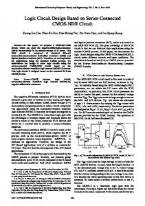
Fig. 1: Feedback equalizer (designed using a variable threshold inverter [17]) can be combined with a traditional master-slave flip flop to design an equalized flip flop. (FEST) to suppress the intersymbol interference (ISI) resulting from aggressive voltage scaling in CMOS digital circuits. Using the FEST circuit, they lower down the critical supply voltage of a 4-bit Kogge-Stone adder as well as a 3-tap 4bit finite impulse response (FIR) filter leading to 20% and 40% decrease in the total consumed energy, respectively. We use the equalization technique developed in [15] for designing logic circuits in sub-threshold regime. The authors in [16] proposed an equalized pass-transistor logic (E-PTL) design technique which consumes between 15% to 30% lower energy per operation than PTL and static CMOS logic, respectively. We propose a circuit-level scheme that uses a communications-inspired feedback equalization technique in the critical path to mitigate the timing errors rising from aggressive voltage scaling in sub-threshold digital logic circuits. It should be noted that we are not designing sub-threshold communication circuits. We are proposing the design of sub-threshold logic circuits that leverage principles of communication theory. Using feedback equalizer circuits, we further scale down the operating voltage of the sub-threshold circuit to decrease the dynamic energy as well as the leakage energy in sub-threshold CMOS circuits. We also propose to increase the operating frequency of the sub-threshold circuits at the fixed supply voltage to reduce the leakage energy. III. E QUALIZED F LIP FLOP VERSUS C ONVENTIONAL F LIP FLOP
In this section, we first explain the use of the feedback equalizer circuit in the design of an equalized flip flop and then provide a detailed comparison of the equalized flip flop with a conventional flip flop in terms of area, setup time and performance. We propose the application of a feedback equalizer (designed using a variable threshold inverter [17] shown in Figure 1) along with the classic master-slave positive edgetriggered flip flop [18] to implement an equalized flip flop. The equalized flip flop dynamically modifies the switching threshold of the gate before the flip flop based on the previous sampled data. If the previous output of the gate is a zero, the equalized flip flop lowers down the switching threshold which speeds up the transition to one. Similarly if the previous output is one, the equalized flip flop increases the switching threshold which speeds up the transition to zero. In this configuration, the circuit adjusts the switching threshold and facilitates faster
Supply voltage (mV)
Propagation delay NE-logic (nsec)
Propagation delay E-logic (nsec)
tc−q NE-flip flop (nsec)
tc−q E-flip flop (nsec)
Setup time NE-flip flop (nsec)
Setup time E-flip flop (nsec)
350 330 310 290 270 250
255 378 532 842 1159 1820
226 336 489 750 1064 1661
3.82 5.66 8.23 12.61 17.87 27.89
3.85 5.72 8.30 12.72 18.04 28.15
6.07 9.01 13.11 20.09 28.49 44.46
8.62 12.80 18.62 28.55 40.49 63.20
TABLE I: Comparison between the characteristics of the equalized flip flop (E-flip flop) with the conventional non-equalized master-slave flip flop (NE-flip flop) at different supply voltages operating in sub-threshold regime. Feedback equalization technique reduces the propagation delay of the 8-bit carry-lookahead adder CMOS logic whereas the setup time and tc−q delay of the conventional flip flop is smaller than the equalized flip flip.
(1)
In Equation (1), EDY N and EL are the dynamic and leakage energy components, respectively. Cef f is the total capacitance of the entire circuit, VDD is the supply voltage and TD = 1/f is the total delay along the critical path of the digital logic block. Feedback equalization enables us to reduce the delay of the critical path in the digital logic block, which in turn reduces the leakage energy. In Equation (1), Ileak is the leakage current and can be written as
����� �
���
���
� �
����
���
���� � � �
�
�� �� �� ������
���
����
���
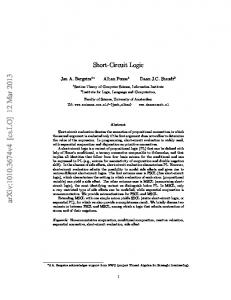
Fig. 2: DC response of the variable threshold circuit in subthreshold regime. The switching threshold of the inverter is modified based on the previous sampled output data. � � � � � �������� �
2 + Ileak VDD TD ET = EDY N + EL = Cef f VDD
��� ��������������� ������ ��� ��������������� ������ ��� �������� �� ������
�� �� �� ������
high-to-low and low-to-high transitions. The DC response of the feedback equalizer circuit in sub-threshold regime is shown in Figure 2. The switching of the variable threshold inverter is dynamically adjusted based on the previous sampled output data. Compared to the above-threshold regime, the reduced noise margin in weak inversion region does not allow for aggressive overscaling of the supply voltage while using the variable threshold inverter. The equalized flip flop has 6 transistors more than the conventional master-slave positive edgetriggered flip flop [18]. Compared to a classic master-slave flip flop with 22 transistors (7 inverters and 4 transmission gates (T G)), the area overhead of the equalized flip flop is around 27%. This area overhead gets amortized across the critical path of the sub-threshold logic. The total energy consumed by a digital circuit in the subthreshold regime can be calculated using
� � � � � � � � � ��
� �
� �
� �
� �
� � � ����� ����
� �
�
�
�
(2)
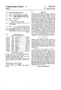
Fig. 3: Comparison between the timing waveforms of the clock signal (A), input node of the conventional flip flop (B), output node of the conventional flip flop (C), input node of the equalized flip flop (D), output node of the equalized flip flop (E). Feedback circuit makes sharper transitions in the waveforms of the logic output node helping the equalized flip flop sample the correct data.
In Equation (2), VT is the transistor threshold voltage, Vth is the thermal voltage, n is the sub-threshold slope factor and η is the DIBL coefficient. There is an exponential relationship between the leakage current and the supply voltage (due to the DIBL effect and for VDS ≈ VDD ). Using the equalized flip flop, we can scale down the supply voltage while maintaining the zero word error rate at a given operating frequency and achieve lower dynamic energy consumption (due to the quadratic relationship between the dynamic energy and the supply voltage) as well as lower leakage energy (due to smaller DIBL effect which exponentially decreases the leakage current). Similar to the area overhead, the dynamic energy as well as the leakage energy overhead of the variable threshold
inverter gets amortized across the entire sub-threshold combinational logic block. Figure 3 illustrates the timing waveforms of the output carry bit of an 8-bit carry-lookahead adder implemented in UMC 130 nm process using static complementary CMOS logic. In the Figure, we show the waveform of clock signal, the input node of the non-equalized flip flop (NE-flip flop), the input node of the equalized flip flop (E-flip flop) and the latched output for both cases. Compared to the signal at the input node of the non-equalized flip flop, the variable threshold circuit provides sharper transitions and decreases the propagation delay of the critical path of the sub-threshold logic. However, it should be noted that excessive positive feedback might lead to increased glitches at the input of the equalized flip flop
Ileak = μ0 Cox
ηVDS −VT W 2 (n − 1)Vth e nVth L
������������ �� �� �
7
NE−logic E−logic
�
� ��������������
Frequency (Hz)
10
6
10
250
260
270
280
290
V
300 310 (mV)
320
330
340
350
DD
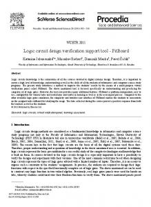
Fig. 4: Operating frequency of the 8-bit carry lookahead adder for zero word error rate as function of different sub-threshold supply voltages. The equalized logic (E-logic) can run 22.87% (on average) faster than the non-equalized logic (NE-logic). which increases the probability of occurrence of timing errors. Therefore, the transistors in variable threshold inverter need to be precisely sized to avoid the errors rising due to the glitches. The setup time of the conventional master-slave positive edge-triggered flip flop [18] is tsetup = 3tinv + tT G . Since the equalized flip flop uses an extra variable-threshold inverter at its output, the setup time of the equalized flip flop will be larger tsetup ≈ 4tinv +tT G . The tc−q delay of the conventional flip flop is tc−q = tinv + tT G . Since the equalized flip flop has the variable threshold inverter as extra load at the output, the tc−q delay of the equalized flip flop is tc−q = tinv + Δt + tT G which is slightly larger than the tc−q delay of the conventional flip flop. Here Δt is the increase in inverter delay due to the extra load. However, the feedback equalizer circuit can significantly lower down the propagation delay of the critical path by providing a faster charging (or discharging) path for the input capacitance of the flip flop. Table I compares the propagation delay, setup time and the tc−q delay of the two 8-bit carry-lookahead adders designed with conventional flip flop and equalized flip flop in UMC 130 nm when operating with different supply voltages. The variable threshold inverter has been accurately sized to minimize the total delay of the critical path. IV. E VALUATION In this section, we perform a detailed comparison, in terms of performance and energy consumption, of a sample 8-bit carry-lookahead adder designed in UMC 130 nm process using both equalized and non-equalized flip flops. We analyze the impact of the proposed feedback equalization technique when the frequency of the sub-threshold logic is improved at a fixed supply voltage and also when the energy of the subthreshold logic is reduced by scaling down the supply voltage at a fixed operating frequency. We also explore the use of the proposed feedback equalizer circuit to reduce the amount of transistor oversizing for mitigating the process variation effects. A. Performance improvement at the fixed supply voltage We first explore the case where the feedback equalizer circuit reduces the rise/fall time of the last gate and hence the delay of the critical path of the combinational logic block
� �
�
� ���
���!�� ������" ����#�� $�!%!��� ������" ����#�� �� !�#�� ������" ����#�� ���!�� ������ ����#�� $�!%!��� ������ ����#�� �� !�#�� ������ ����#��
���
���
���
���
��� � � ��� ����
���
���
� �
���
Fig. 5: Comparison between the total consumed energy as well as the dynamic/leakage components of the 8-bit carry lookahead adder for different supply voltages. Operating at the respective minimum energy supply voltage, the equalized logic is burning 18.4% less total energy compared to the nonequalized logic. leading to a higher operating frequency. The variable threshold inverter can be used to reduce the propagation delay of the critical path at any operating supply voltage. Figure 4 shows the operating frequency of the 8-bit carry lookahead adder for different sub-threshold supply voltages at zero word error rate when using an equalized and a conventional flip flop. Here, we determined the optimum sizing for the feedback equalizer circuit that minimizes the propagation delay of the critical path and avoids sampling of glitches to achieve zero error rate operation at each supply voltage. The sizing of the combinational logic block is the same for both the equalized and non-equalized circuit and is determined using the design methodology described in [3] to address the degraded noise margin levels in sub-threshold regime. The operating frequency of the equalized logic is 22.87% (on average) higher than the non-equalized logic over the range of 250 mV to 350 mV . The amount of performance acceleration in aggressively scaled supply voltages is more promising compared to voltages close to the threshold as the variable threshold inverter is capable of significantly decreasing the large transition times of the logic designed in the deep sub-threshold region. At 250 mV supply voltage, the equalized flip flop improves the operating frequency of the logic by 27.8% whereas the amount of performance improvement at 350 mV is 16.2%. By reducing the propagation delay of the critical path, the feedback equalizer circuit is capable of reducing the dominant leakage energy of the digital logic in sub-threshold regime. Figure 5 illustrates a head-to-head comparison between the total energy, the dynamic energy and the leakage energy of the 8-bit carry lookahead adder for different supply voltages while using the equalized or conventional non-equalized flip flops. By adding the feedback equalizer to the conventional flip flop, the dynamic energy of the logic with the equalized flip flop is 3.47% (on average) larger than the logic designed with nonequalized conventional flip flop. This is negligible compared to the 22.6% reduction in the leakage component of the design. The feedback circuit drops the minimum energy supply voltage of the equalized logic by 10 mV while maintaining the zero word error rate operation. If operated at the respective minimum energy supply voltage, the equalized logic consumes
1.28 1.22 0.64 0.4 0.52
1.62 1.49 0.71 0.47 0.66
TABLE II: Comparison between the minimum energy point and the corresponding operating frequency of the equalized logic (E-logic) vs. non-equalized (NE-logic) design of various logic blocks. 18.4% less total energy compared to the non-equalized logic and runs 5.12% faster. If both designs are operated at the minimum energy supply voltage of the non-equalized logic, the equalized logic runs 26% faster and consumes close to 18% less energy. Decreasing the dominant leakage energy component of the sub-threshold logic together with reducing the propagation delay of the critical path, the feedback equalization technique lowers the energy-delay product of the logic designed in weak inversion region. On average, the equalized 8-bit carry lookahead adder has 30.44% smaller energy-delay product value compared to the non-equalized logic over the range of 250 mV to 350 mV for zero word error rate operation. If we compare the energy-delay product at the respective minimum energy supply voltages, the equalized flip flop reduces the energy-delay product of the 8-bit carry lookahead adder by 35.4%. Table II compares the minimum energy point and the corresponding operating frequency of the equalized logic design (E-logic) vs. non-equalized logic design (NE-logic) of an 8-bit Carry-lookahead adder (CLA), 8-bit Array Multiplier, 3-tap 8-bit FIR filter, 16-bit Ripple-carry adder (RCA) and 16-bit Carry-select adder (CSA) all designed in UMC 130 nm process. On an average, the equalization technique has 24.97% lower energy-delay product than the non-equalized logic design. B. Leakage reduction at the fixed operating frequency As described in Section III, the equalized flip flop can be used to scale supply voltages (while maintaining the operating frequency) to lower down the dominant leakage energy by decreasing the leakage current of the sub-threshold logic. We designed the feedback equalizer circuit for each scaled supply voltage that ensured the reliable operation of the equalized design without any timing error. Figure 6 illustrates the dynamic and leakage energy components of the 8-bit carry lookahead adder at the minimum energy supply voltage (of the nonequalized design) and below when the operating frequency of all design points with zero word error rate is f = 1.28 M Hz (the frequency of the minimum energy supply voltage for the non-equalized design). Compared to the non-equalized design, the equalized design can operate at 30 mV lower supply voltage leading to 16.72% lower energy consumption. The equalized design cannot operate for VDD < 270mV due to timing errors resulting from increased rise/fall times.
10 8 6 4 2 0 VDD (mV)
E− 3 lo 00 gi c
10.3 15.24 94.84 34.7 80.6
Dynamic Component Leakage Component
N
12.63 16.27 100.32 37.81 89.8
12
E− 2 lo 90 gi c
8-bit CLA 8-bit Multiplier 8-bit FIR filter 16-bit RCA 16-bit CSA
14
E− 2 lo 80 gi c
E-logic Frequency (MHz)
E− 2 lo 70 gi c
NE-logic Frequency (MHz)
Energy (fJ/cycle)
E-logic Energy (fJ/cycle)
Fig. 6: Comparison between the energy consumed by the equalized (E-logic) vs. non-equalized (NE-logic) 8-bit carry lookahead adder for different supply voltages with fixed performance (f = 1.28 M Hz) at zero word error rate. The non-equalized logic design consumes minimum energy at 300 mV . The equalized flip flop enables 30 mV supply voltage scaling leading to 16.72% lower total consumed energy. The equalized flip flop cannot operate at VDD < 270mV due to the occurrence of timing errors. 40 Energy−delay product (fJ.µsec)
Logic block
NE-logic Energy (fJ/cycle)
Baseline design (Wbaseline) 95% × Wbaseline 85% × W
30
baseline
75% × W
baseline
20
10
0 0.25
0.26
0.27
0.28
0.29
V
0.3 0.31 (V)
0.32
0.33
0.34
0.35
DD
Fig. 7: Energy-delay product of the scaled-down equalized 8bit carry lookahead adder for zero word error rate operation. We can achieve reliable operation even when the transistors in the equalized logic design are scaled down to as small as 75%×Wbaseline . C. Mitigating process variations Using the proposed feedback-based technique, the critical sizing approach used for designing the sub-threshold logic circuits in [3] can be relaxed. The transistor sizing can be scaled down while ensuring the reliable operation using feedback equalizer circuit in presence of process variations. For the 8-bit carry-lookahead adder in UMC 130 nm process, the transistors sized using [3] (Wbaseline ) can be scaled down to 75%×Wbaseline while matching the operating frequency of the equalized design and non-equalized design. Figure 7 illustrates the energy-delay product of the scaled down equalized logic and baseline non-equalized logic for different sub-threshold supply voltages. At a given voltage, compared to the nonequalized design, the equalized design uses smaller transistors and has lower propagation delay resulting in a reduction of both dynamic and leakage energy. For a 3σVT = 30mV systematic variability in threshold voltage, the equalized design can reliably operate without the occurrence of any timing errors. Table III summarizes the amount of energy savings of the equalized logic with scaled down transistors compared to the baseline non-equalized and the equalized logic where the baseline logic has been sized according to the method
Scaled-down equalized logic size
Total energy saving w.r.t non-equalized
95%×Wbaseline 85%×Wbaseline 75%×Wbaseline
12.87% 16.79% 20.72%
Total energy saving the prior sampled outputs, the feedback equalization circuit w.r.t equalized enables a faster switching of the logic gate outputs and 6.72% 10.92% 15.12%
TABLE III: Energy savings in scaled-down equalized logic compared to baseline non-equalized and equalized logic at the minimum energy supply voltage with zero word error rate operation. Energy−delay product (fJ.µsec)
1.4 1.2
NE−logic E−logic
1 0.8 0.6 0.4 0.2 0
45
65 90 Technology node (nm)
130
Fig. 8: Energy-delay product of a 8-bit carry lookahead adder designed using equalized logic (E-logic) vs. non-equalized logic (NE-logic) at zero word error rate at different technology nodes. The equalized logic approach reduces the energy-delay product of the sub-threshold logic by up to 26.46% across all technology nodes in the minimum energy supply voltage. proposed in [3]. Overall the feedback equalization along with transistor size scaling consumes up to 20.72% lower total energy compared to the conventional non-equalized design in sub-threshold regime. V. E FFECT OF T ECHNOLOGY S CALING In this section, we analyze the effect of technology scaling on the performance improvement and the energy reduction obtained using feedback equalization technique in sub-threshold regime. In scaled technology nodes, the contribution of leakage energy component dominates due to larger DIBL effect as well as smaller VT values. Running the sub-threshold logic faster, the equalizer will more effectively reduce the leakage energy component and in turn decrease the energy-delay product in scaled technology nodes. Figure 8 illustrates the value of the energy-delay product of the 8-bit carry lookahead adder designed using PTM [19] for 4 different technology nodes and operating at zero word error rate at minimum energy supply voltage. Compared to the non-equalized logic design, the energy-delay product of the equalized logic design is 20.45%, 24.32%, 27.82% and 33.25% smaller in 130 nm, 90 nm, 65 nm and 45 nm technology nodes, respectively. On average, the equalized flip flop reduces the energy-delay product of the sub-threshold logic by up to 26.46% across all technology nodes at the minimum energy supply voltage. VI. C ONCLUSION We proposed the application of a variable threshold inverterbased feedback equalization circuit to reduce the dominant leakage energy of the digital CMOS logic operating in subthreshold regime. Adjusting the switching thresholds based on
provides the opportunity to reduce the leakage current in weak inversion region. We implemented a non-equalized and an equalized design of an 8-bit carry lookahead adder in UMC 130 nm process using static complementary CMOS logic and managed to reduce the propagation delay of the critical path of the sub-threshold logic and correspondingly lower the dominant leakage energy, leading to 35.4% decrease in energy-delay product of the conventional non-equalized design at minimum energy supply voltage. In an alternate design approach, using the feedback equalizer circuit, we obtained 16.72% reduction in energy through voltage scaling while maintaining an operating frequency of 1.28 M Hz. We also showed that the equalized sub-threshold 8-bit carry lookahead adder requires lower upsizing to tolerate process variation effects leading to 20.72% lower total energy. R EFERENCES [1] A. Wang and A. Chandrakasan, “A 180-mv subthreshold fft processor using a minimum energy design methodology,” Solid-State Circuits, IEEE Journal of, vol. 40, no. 1, pp. 310–319, 2005. [2] M. Pelgrom et al., “Matching properties of mos transistors,” Solid-State Circuits, IEEE Journal of, vol. 24, no. 5, pp. 1433–1439, 1989. [3] J. Kwong et al., “A 65 nm sub-vt microcontroller with integrated sram and switched capacitor dc-dc converter,” Solid-State Circuits, IEEE Journal of, vol. 44, no. 1, pp. 115–126, 2009. [4] N. Verma et al., “Nanometer mosfet variation in minimum energy subthreshold circuits,” Electron Devices, IEEE Transactions on, vol. 55, no. 1, pp. 163–174, 2008. [5] B. Zhai et al., “Analysis and mitigation of variability in subthreshold design,” in Proc. ISLPED, 2005, pp. 20–25. [6] S.-H. Choi et al., “Novel sizing algorithm for yield improvement under process variation in nanometer technology,” in Proc. DAC, 2004, pp. 454–459. [7] H. Kaul et al., “Near-threshold voltage (ntv) design-opportunities and challenges,” in Proc. DAC, 2012, pp. 1149–1154. [8] J. Zhou et al., “A 40 nm inverse-narrow-width-effect-aware subthreshold standard cell library,” in Proc. DAC, 2011, pp. 441–446. [9] B. Liu et al., “Standard cell sizing for subthreshold operation,” in Proc. DAC, 2012, pp. 962–967. [10] N. Jayakumar and S. Khatri, “A variation-tolerant sub-threshold design approach,” in Design Automation Conference, 2005. Proceedings. 42nd, 2005, pp. 716–719. [11] B. Liu, H. Pourshaghaghi, S. Londono, and J. de Gyvez, “Process variation reduction for cmos logic operating at sub-threshold supply voltage,” in Digital System Design (DSD), 2011 14th Euromicro Conference on, 2011, pp. 135–139. [12] B. Mishra, B. Al-Hashimi, and M. Zwolinski, “Variation resilient adaptive controller for subthreshold circuits,” in Design, Automation Test in Europe Conference Exhibition, 2009. DATE ’09., 2009, pp. 142–147. [13] G. De Vita and G. Iannaccone, “A voltage regulator for subthreshold logic with low sensitivity to temperature and process variations,” in Proc. ISSCC, 2007, pp. 530–620. [14] S. Luetkemeier et al., “A 200mv 32b subthreshold processor with adaptive supply voltage control,” in Proc. ISSCC, 2012, pp. 484–486. [15] Z. Takhirov et al., “Error mitigation in digital logic using a feedback equalization with schmitt trigger (fest) circuit,” in Proc. ISQED, 2012, pp. 312–319. [16] ——, “Energy-efficient pass-transistor-logic using decision feedback equalization,” in Proc. ISLPED, 2013, pp. 335–340. [17] S. Sridhara et al., “Joint equalization and coding for on-chip bus communication,” VLSI Systems, IEEE Trans. on, vol. 16, no. 3, pp. 314– 318, 2008. [18] J. Rabaey, A. Chandrakasan, and B. Nikoli´c, Digital Integrated Circuits. Pearson Education, 2003. [19] (2011) Predictive technology model. [Online]. Available: http://ptm.asu. edu/