1
Threshold Logic Computing: Memristive-CMOS Circuits for Fast Fourier Transform and Vedic Multiplication Alex Pappachen James, Dinesh S. Kumar, and Arun Ajayan Abstract—Brain inspired circuits can provide an alternative solution to implement computing architectures taking advantage of fault tolerance and generalisation ability of logic gates. In this brief, we advance over the memristive threshold circuit configuration consisting of memristive averaging circuit in combination with operational amplifier and/or CMOS inverters in application to realizing complex computing circuits. The developed memristive threshold logic gates are used for designing FFT and multiplication circuits useful for modern microprocessors. Overall, the proposed threshold logic outperforms previous memristive-CMOS logic cells on every aspect, however, indicate a lower chip area, lower THD, and controllable leakage power, but a higher power dissipation with respect to CMOS logic. Index Terms—Threshold logic, memristors, digital circuits, digital integrated circuits, programmable circuits
I. I N T RO D U C T I O N There has been several attempts to functionally and electrically mimic the neuron activity and its networks [1]. However, major challenge that deters the progress in VLSI implementations of brain like logic gates is the scalability of the networks and its practical limitations in solving large variable boolean logic problems. The possibility to mimic the brain like circuits and logic networks is a topic of intense debate. One possibility is to apply the threshold logic gates in designing conventional computational blocks, while other option is to develop a completely trainable architecture that does not strictly bind itself to conventional computing topologies. In this brief, we restrict the notion of the brain mimicking to develop a generalised memristive threshold logic cell in application to designing conventional computing blocks. Nonetheless, this topic is one of the forefront challenges in development of on-chip brain computing, and would require us to investigate not just new circuit design logic, but also new devices and systems. Threshold logic is the primary logic of human brain that inspires from the neuronal firing and training mechanisms. The progress in threshold logic circuits [2] are often limited to implementation of logic gates with few number of input variables, this leads to limited progress being made in the development of practical computing circuit topologies. Memristor like switching devices [3] unlike many other electronic devices has an interesting appeal in on-chip brain computing, as it offers switching state through its bi-level resistance values. Further these resistors are mapped to the binary memory space and offer the advantage of low on-chip area and low leakage currents. We explore this aspect of memristor, and extend over our previous work [4] in designing FFT computing useful for signal processing applications, and vedic additions and multiplications for efficient ALU design. The resulting circuits can be used in combination with conventional CMOS circuits to develop threshold logic processor designs. II. C O M P U T I N G C I R C U I T S
W I TH
T HR ES H O LD L O GI C
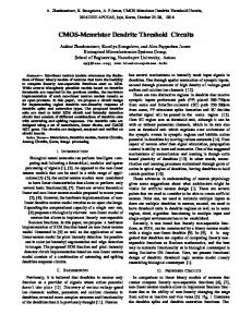
The memristive threshold logic (MTL) cell shown in Fig. 1 is the basic cell which consists of two parts; a memristor based input A.P. James is a faculty with Electrical and Electronic Engineering department, Nazarbayev University. D.S. Kumar and A. Ajayan are member research staff with Enview R&D labs. Contact Email:
[email protected] Manuscript received Oct. 7, 2013; revised Feb. 16, 2014; July 14, 2014; 12 Oct., 2014.
Fig. 1: Memristive threshold logic cell
voltage averaging circuit and an output threshold circuit. In contrast to our previous work on resistive threshold logic [4], the proposed cell has the input potential divider circuit modified by removing the pull-down resistor to form an input voltage averaging circuit and the threshold circuit modified with the combined use of operational amplifier and CMOS inverter. In particular, by removing the pulldown resistor from [4], an important improvement over lower power dissipation is achieved in cell as shown in the Table I. In the presented work, the threshold unit consisting of a combination of an op-amp [5] and a CMOS inverter that allows for fault tolerance in terms of logical output signal stability. The generalization of the cell to work as different logic gates is achieved with the ability of the cell to utilize a wider range of threshold value. TABLE I: C O M PA R I N G P R E V I O U S C I R C U I T [4] W I T H P R E S E N T P RO P O S E D C I R C U I T B Y I M P L E M E N T I N G A 2- I N P U T NOR L O G I C G AT E . Logic Family
Power dissipation (μW)
RTL without op-amp [4] MTL without op-amp RTL with op-amp [4] MTL with op-amp
8.30 3.00 19.70 16.61
For an N input cell, the resistance circuit part consist of N memristors having equal memristance values, M1 = M2 = ...MN = M . The output PN voltage VA for N input voltages VI can be represented as VA = ( I =1 VI )/N . Table II shows truth table for two input NAND and NOR gates. V1 and V2 are the input voltage that can take values of VL (voltage low) or VH (voltage high). For practical purposes, the boundary conditions are avoided, and in general for any N inputs, if VREF is in between ((N − 1)VH + VL )/N and VH we obtain NAND logic and if it is in between VL and (VL + (N − 1)VH )/N we obtain NOR logic. The combined effect of VREF at operational amplifier and VT H of the inverter provides a stable threshold logic unit, where VT H is the threshold voltage of the inverter. The operational amplifier ensures a wider range of threshold value limiting the role of inverter as a means to ensure stable binary states. The impact of having operational amplifier in the output of the cell is shown in Fig. 2a, while Fig. 2b captures the variations of the output voltage for different values of VREF . The advantages of using opamp in order to fix the threshold of the circuit can be clearly observed. from the Fig. 2. Only for the gates that having inputs higher than 2 input require the use an op-amp in the circuit. In addition to this It has been observed during simulation that, without using an op-amp in the circuit and a +/-15% variability in channel lengths does not have any effect on the output of NAND logic, while minor variations in NOR logic. On the contrary, we observed no variation in outputs even with +/-15% variability in channel lengths when op-amps are incorporated. The reason for this is because the amplification in the voltage range made by the op-amp increases the voltage range to +/1. This offers broader selection range of CMOS inverters thresholds ensuring that the threshold values lie inside this range even if the
2
(a)
(b)
Fig. 2: Relation between output of the memristive divider and output of the inverter of the proposed cell. (a) shows the effect of op-amp on the output of the cell, and (b) shows the variation in output of the cell for different values of VREF .
(a) NAND
(b) NOR
Fig. 3: The graphs illustrate the effect of change in the technology length on the output of MTL logic family without op-amp.
technology length are changed. Additionally change in the speed of the transistors will reflect in the delay introduced by inverter, i.e., slow-slow (0.89ns), fast-fast (0.23ns), slow-fast (0.50ns), fast-slow (0.52ns) tested with an input pulse with speed of 10ns. The delay is high for the slow-slow condition and less in-case of fast-fast. Fig. 3 shows the effect of change in technology length on the output of MTL logic gates. While checking the effect of other process variations, temperature and chain of logic gates, it is observed that the power dissipation has a linear change in accordance with the temperature change and has no effect by the chain of logic gates. In case of delay, change in temperature doesn’t have any significant effect but the chain of logic gates will increase the delay linearly with an increase of d1 in each level, where d1 is the delay of a single cell. For this study, inverter configuration of the proposed cell is used and a chain of 6 inverters are checked in order to get the effect of chain of logic gates. The results are shown in the Fig. 4. Throughout this paper, we use the non-ideal resistive switching model of memristor reported in [4] for our study with an area of 10nm × 10nm and resistances in the range of [10−6 Ω, 10−12 Ω], while CMOS circuits uses 0.25 μm (both in the MTL and CMOS logics)
(a)
(b)
Fig. 4: The graphs show the effects of (a) changes in temperature, and (b) delay introduced by chain of logic gates on power dissipation and delay.
(a)
(b)
Fig. 5: Operating range of two input (a) NOR cell (b) NAND memristive threshold logic cell with VREF = 0.5V .
TSMC (Taiwan Semiconductor Manufacturing Company) technology to reflect the practical applicability in standard silicon technologies. The SPICE (Simulation Program with Integrated Circuit Emphasis) models take into account the extracted parasitics from CMOS layout, so as to ensure the accuracy for practical realisation. Memristor model has a non-ideal behaviour and take into account the boundary effects. In practise, the memristor and CMOS layers can be separated into different layers [6], [7]. Memristors can be fabricated directly above the CMOS circuits by making them as a part of the interconnect. A 2D array of vias provides electrical connectivity between the CMOS and the memristor layers. Since the variability between the memristors are practically limited and there is a large threshold range for VREF for achieving desired logical functionality, the errors resulting from memristance tolerance can be ignored. TABLE II: T RU T H TA B L E LO GIC CE LL V1 VL VL VH VH 1 2
V2 VL VH VL VH
FO R T HE
VA VL +VL 2 VL +VH 2 VH +VL 2 VH +VH 2
MEMR I S TI VE T H R ES HO LD NOR VH VL VL VL
1
NAND VH VH VH VL
2
(N −1)V +V
L H N input NOR threshold: VL