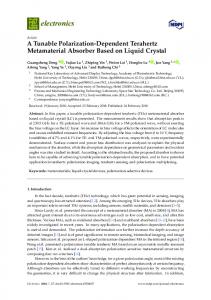
TUNABLE MEMS FILTER REALIZATION USING METAMATERIAL STRUCTURES S. Das1, A. Kundu1, S. Chatterjee1, B. Gupta1, and H. Saha2* 1. IC Design and Fabrication Center, Department of ETCE, Jadavpur University, Kolkata: 700032 2. Center of Excellence for Green Energy and Sensor Systems, Bengal Engineering and Science University, Howrah: 711103 *corresponding author:
[email protected] Abstract: A stop-band filter with tuning capability is presented on a transmission line implemented using complementary split ring resonator (CSRR) and Radio Frequency Micro Electro Mechanical Systems (RF MEMS) varactor. The rejection in the stop-band is -55dB at the centre frequency of 15GHz. The RF MEMS capacitor provides an option of achieving the tunability of the filter. 1. INTRODUCTION Recent advances in the field of electromagnetic theory have led to the emergence of new kind of artificial materials called Metamaterials which may be formed by using novel structures like split ring resonators (SRRs), complementary split ring resonators (CSRRs) etc.[1]. They are designed to obtain controllable properties in the fields of electromagnetics or optics. Metamaterial transmission lines (t-lines) are nothing but host tlines loaded with metamaterial structures. Reactive elements can be embedded on the t-line using a (i) CL loaded approach or (ii) resonant type approach [2, 3]. The advantage of using resonator loaded t-line for filter design is that they are significantly smaller in size (generally less than one-tenth of a wavelength) than conventional resonator structures enabling the design of very compact filters. The small size and controllability of the electrical characteristics of metamaterial t-lines employing SRRs or CSRRs are the main properties to synthesize microwave filters with compact dimensions and exceptional features. This is due to the inherent resonance characteristics of SRRs/CSRRs which enables the filter to have a sharp cut off around the resonance frequency [4, 5]. As both SRRs and CSRRs can be implemented by planar IC technology [4], an added advantage of CMOS compatibility may also be achieved. Very recently, the use of MEMS capacitors with metamaterials has been suggested for the design of tunable filters [2]. The research is still in a very nascent state and much work needs to be done for optimizing the system for the desired applications. The MEMS based variable capacitors may be employed over the SRR/CSRR embedded transmission lines to achieve tunability based on the up and down states of the MEMS capacitor. Such tunable SRR/CSRR loaded metamaterial transmission lines based on varactors may be applied in the design of reconfigurable antennas, phase shifters and matching networks [4]. In this paper, we present a CSRR embedded CPW transmission line on silicon substrate with a MEMS
capacitor. To the best of our knowledge it is the first time that such design has been carried out on silicon substrate to allow CMOS compatibility. The CSRR is etched on the signal strip of the CPW which enables the structure to behave as a band-stop filter. The proposed structure is simulated using ANSOFT HFSS v11®. Results pertaining to the MEMS capacitor in the up state are presented here and it is observed that good rejection is obtained around the centre frequency with acceptable insertion loss in allowed band. The electromechanical characterization of the MEMS capacitor suspended over the CSRR embedded CPW transmission line has been performed using INTELLISUITE v8.5®. Further, we also suggest for the first time an equivalent circuit model of the structure which not only provides an insight into the system but also helps in its optimization. The structure proposed is a proof-of-concept and although tuning has not been demonstrated as a part of this work the authors believe that on selecting proper design parameters a tunable filter with a tuning range around 15-20% is possible. This may be achieved by placing multiple CSRRs loaded with MEMS capacitors in cascade as mentioned in Section 4.2. 2. PROPOSED DEVICE STRUCTURE Fig. 1(a) and 1(b) show the top view and cross section of the CSRR embedded CPW with a MEMS capacitor. A CPW configuration corresponding to W/S/W of 60/100/60 is chosen to obtain 50ohm characteristic impedance. The CSRR is patterned on the CPW central line which is housed on an oxidized high resistivity silicon substrate. The CPW transmission line is made of Al (1µm thick) which allows for the native Al oxide to act as a dielectric between the CPW and the MEMS bridge. This dielectric acts as an isolator between the two when a voltage is applied to pull the bridge down. The MEMS bridge is suspended at an air gap of g0 and has dimensions of length, width and thickness given by l, w and t respectively. The length of the CSRR and width of the rings is given by L and c
respectively. The spacing between the rings and the split on the rings is d and g respectively.
Fig. 1(a): Top view of a CSRR/RF MEMS varactor loaded CPW t-line.
appropriately for rectangular CSRR in the proposed structure through simulations in Ansoft HFSS v11®.
Fig. 1(b): Cross sectional view of the CSRR/RF MEMS loaded CPW transmission line.
3. PROPOSED DEVICE DESIGN The design starts by selecting a suitable CPW for obtaining 50ohm characteristic impedance (Z0). Here we report a single rectangular shaped CSRR etched onto the signal line of the CPW. The length of the CSRR (L) is very crucial for obtaining proper filtering actions. For a centre frequency of 15GHz it is seen that the length of a unit cell (p) would be around 2000µm according to [6]
p = λg / 4.........................(1)
where λg is the guided wavelength and is given by
λg = λ0 / ε eff ..................(2) where εeff is the effective permittivity and is approximately given by
(a) (b) Fig. 2: (a) Representation of CSRR. (b) Equivalent circuit of CSRR
ε eff = (ε r + 1) / 2...............(3)
where εr is the relative permittivity of the substrate which is 11.9 for silicon. A CSRR essentially consists of two concentric split rings etched on a metallic surface as shown in Fig. 2(a). It is obtained from the idea of applying Babinet’s principle to the SRR [4]. According to this principle, in such complementary structures, the electric, magnetic fields, currents interchange their roles [4]. The equivalent circuit of the CSRR can thus be represented as in Fig 2(b). the values of Lc and Cc are given by
Lc = 2π rLpul .......................(4)
Cc = 2π rC pul ......................(5) where Lpul is the per-unit-length inductance of the CPWs connecting the inner disk to the ground, r=(rext-c-d/2) is the mean radius of the CSRR and Cpul is the per unit length capacitance along the slot between the rings. The formulas have been modified
Fig. 3: Proposed equivalent model of CSRR loaded CPW t-line with MEMS varactor. The analysis of MEMS varactor based CSRR loaded CPW t-lines are still an area which needs intensive research. The authors believe that the structure may be represented by an equivalent model proposed in Fig. 3 to provide a better understanding of the system. The analytical expressions of the different elements of the proposed equivalent model are given below.
= Ct Csubs + Cair ................................(6) where Cair = 4ε 0
K ( k0 ) ............................(7) K ( k '0 )
= Csub 2ε 0 (ε r − 1)
k1 =
K (k1 ) ..................(8) K (k '1 )
structure has been carried out in INTELLISUITE v8.5®. Contact analysis indicates that the actuation voltage (Vp) will be around 28V [Fig. 4]. It should be kept in mind that the actuation area is mainly due to intersection of the bridge with the width (b) along the CSRR embedded CPW t-line. The area due to the widths of the split rings will have a small effect (20% of total area) as it is closer to the anchors.
sinh(π S / 4h) ...........(9) sinh{[π ( S + 2W )] / 4h}
where h is the height of the substrate. ' k= 1
1 − k12 ...............................(10)
k0 =
k= 0
S .............................(11) S + 2W
1 − k ............................(12)
'
2 0
Fig. 4: Static analysis of CSRR loaded CPW with MEMS bridge by INTELLISUITE v8.5®. Fig. 5 shows a plot between the gap height (g) and the applied voltage (V) applied analytically using the equation
Now,
2k
ε eff
V g 2 ( g 0 − g ).......(17) = Ct ................................(13) = ε 0 (1.2bw) Cair The black square in Fig.5 indicates the result
which leads to
Z0 =
1 cCair ε eff
.......................(14)
obtained using FEM simulations and it is seen that they are in good agreement. 2.0µ
and
Lt = Z Ct .................................(15) Cb = ε 0 (1.2bw) / g 0 ...................(16) The proposed device structure has been simulated in standard FEM tools and the results are discussed in the following section. 4. RESULTS AND DISCUSSIONS 4.1 Mechanical characterization
and
electromechanical
4.1.1 Static Analysis The dimensions of the CPW to be chosen are governed by the desired RF performance which is discussed later. It is seen that a bridge length l of 320µm is suitable for the chosen CPW dimensions. The bridge width is optimized from the proposed model keeping in mind the center frequency of the stop- band filter. It is seen that a bridge width w of 80µm gives us the desired performance. The thickness t and height of the bridge g0 has been optimized, to achieve acceptable values of actuation voltage and switching time, to 1µm and 2µm respectively. The static analysis of the proposed
Gap Height (m)
1.5µ
2 0
1.0µ
500.0n
0.0 0.0
5.0
10.0
15.0
20.0
25.0
30.0
Voltage (Volt)
Fig. 5: Plot of gap height vs. voltage to obtain the actuation voltage. The actuation voltage is obtained analytically from the following formula:
Vp =
8kg 03 ..........(18) 27ε 0 (1.2bw)
4.1.2 Transient Analysis The dynamic response of the system is given by d’Alembert’s principle as
1 ε 0 (1.2bw)(1.4V p ) .....(19) 2 ( g 0 − x) 2 2
mx + bx + kx = Fe =
This non- linear differential equation has been solved in MATHEMATICA v5® and a switching time of around 25µs is obtained as shown in Fig. 6.
Table 1: Parameters & Results for Electromechanical Analysis m (ng) b k(N/m) Vp (V) t(µs) g0 (μm) Mass Damping Spring Actn. Sw. Gap coeff. const. voltage time 0.173 4.33x10⁻⁴ 5.8594 28 25 2.0
would like to acknowledge the support and guidance of Prof. D. R. Poddar, Dept. of ETCE, Jadavpur University. 0 -10
S-parameter (dB)
The parameters and results of the electromechanical analysis are summarized in Table 1.
-20 -30 -40 S11 S21
-50 -60 0
5
10
15
20
25
30
Frequency(GHz)
Fig. 6: Transient analysis of CSRR/RF MEMS loaded CPW
Fig. 7: Simulated S-parameters for the proposed structure with MEMS capacitor in the up-state.
4.2 RF characterization The choice of the dimensions for the CSRR is very crucial for obtaining the desired performance. As already discussed the length of the CSRR is chosen as 2000µm. The width of the rings, spacing between the rings and the split in the rings have been optimized to 10µm, 10µm and 5µm respectively. Optimization has been done with the help of the proposed model and FEM simulation using ANSOFT HFSS v11®. Fig. 7 shows the simulated sparameters for the MEMS capacitor in the up- state. It is seen that the rejection in the stop- band is around -55dB with an insertion loss of around -0.5dB in the allowed bands. Work is still going on to obtain tunability using the proposed structure. The use of multiple CSRRs loaded with MEMS capacitors may help in achieving the same [Fig. 8]. 5. CONCLUSIONS A CSRR embedded CPW t-line loaded with a MEMS capacitor is presented for tunable filter designs on silicon substrate. An equivalent model of the structure is presented for the first time which provides an understanding of the system behavior. Work is going on for the design and modeling of the complete tunable filter. The use of MEMS in metamaterials is an entirely new concept and fabrication and characterization of such structures is an interesting area for research. ACKNOWLEDGEMENT The authors would like to acknowledge the National Programme on Micro and Smart Systems for providing the necessary support. Ms. Sonali Das
Fig. 8: CPW t-line loaded with multiple CSRRs and MEMS capacitors. REFERENCES [1]Ricardo Marques,Ferran Martin and Mario Sorolla,“Metamaterials with Negative Parameters, Theory, Design and Microwave applications” [2] I. Gil, F.Martin, X. Rottenberg and W. De Raedt, “Tunable stop-band filter at Q-band based on RF MEMS metamaterials,” Electronic Letters, 2007, vol. 43, no. 21. [3]F. Aznar, M. Gil, J. Bonache and F. Martin, “modelling metamaterial transmission lines: a review and recent developments”,Opto-electron review,2008, Vol 16, No. 3, pp 226-236 [4]Marta Gil Barba, Doctoral Thesis, “Resonant-type metamaterial transmission lines and their application to microwave device design,” 2009 [5] I A I Al-Naib, C Jansen and M Koch, “Miniaturized bandpass filter based on metamaterial resonators: a conceptual study,” J. Phys. D: Appl. Phys. 41 (2008) 205002 (4pp) [6]Christophe Caloz, Tatsuo Itoh, “Electromagnetic metamaterials:transmission line theory and microwave applications: the engineering approach”