Jun 15, 2001 - Using these modes, we can obtain very good coupling between a PBG waveguide and a dielectric slab waveguide with similar slab properties.
PHYSICAL REVIEW B, VOLUME 64, 033308
Guiding mechanisms in dielectric-core photonic-crystal optical waveguides Ali Adibi Georgia Institute of Technology, School of Electrical and Computer Engineering, Atlanta, Georgia 30332
Yong Xu, Reginald K. Lee, Amnon Yariv, and Axel Scherer California Institute of Technology, Departments of Electrical Engineering and Applied Physics, Pasadena, California 91125 共Received 26 February 2001; published 15 June 2001兲 We show that the main guiding mechanisms in dielectric-core photonic crystal optical waveguides are total internal reflection and distributed Bragg reflection. We also show that by placing a slab of semiconductor material between two photonic band gap 共PBG兲 mirrors, we can obtain waveguide modes at frequencies out of the photonic bandgap. These modes are similar to the modes of a conventional dielectric slab waveguide. Using these modes, we can obtain very good coupling between a PBG waveguide and a dielectric slab waveguide with similar slab properties. DOI: 10.1103/PhysRevB.64.033308
PACS number共s兲: 42.70.Qs, 42.79.Gn
Photonic crystals1,2 have inspired a lot of interest recently due to their potential for controlling the propagation of light. Photonic crystals with line defects can be used for guiding light. Several aspects of photonic-crystal waveguides have been recently investigated.3,4 Guiding light through sharp bends has been recently proposed5 and demonstrated at microwave6 and optical7 frequencies. In all the proposals and demonstrations of photonic bandgap 共PBG兲 waveguides, the guiding modes were restricted to the photonic bandgap. In this paper, we show that there also exist some guiding modes outside the photonic bandgap and explain their behavior. We also show that we can couple a conventional dielectric slab waveguide to a PBG waveguide with high transmission coefficient over a wide range of frequencies compared to the photonic bandgap. In this work, we show that the properties of the fundamental mode of a PBG waveguide can be understood as the result of total internal reflection 共similar to a conventional dielectric slab waveguide兲 and distributed Bragg reflection 共due to the presence of the photonic crystal兲. We also show that the range of efficient guiding in a PBG waveguide is not limited to the photonic bandgap. In other words, the presence of an absolute photonic bandgap is not necessary for lossless guiding. The main limitation for the loss-less guiding in a PBG waveguide is the coupling of the guided mode to other nonconfined modes of the photonic-crystal cladding. The absence of photonic-crystal modes with the same frequency and wave vector as those of the guided mode, are necessary for loss-less guiding. Therefore, the main role of a photonic bandgap in dielectric-core PBG waveguides is to provide a frequency range in which there are no other modes that couple to the guided mode. The actual frequency range with this property is usually bigger than the absolute photonic bandgap. Having this fact in mind, we use the phrase ‘‘PBG waveguide’’ to refer to the waveguides made by generating a line defect in a photonic crystal without implying that the guiding mechanism is due to the photonic bandgap 共PBG兲 itself. Efficient coupling of light into and out of a PBG waveguide 共for example, from an optical fiber兲 is important in both performing experiments with PBG waveguides and in designing optical elements using photonic crystals. We show 0163-1829/2001/64共3兲/033308共4兲/$20.00
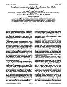
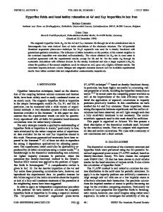
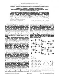
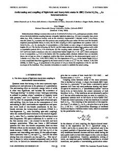
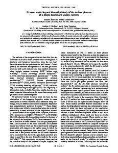
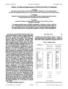
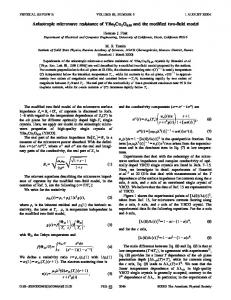
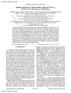
in this paper that a dielectric slab waveguide can be coupled efficiently in a wide frequency range to a PBG waveguide and vice versa. Methods for efficient coupling of light into and out of a dielectric slab waveguide 共from a fiber or from free space兲 are well known. For example, tapered slab waveguide can be used for optimizing the coupling efficiency. Therefore, our results suggest that we can use dielectric slab waveguides for coupling light into and out of PBG waveguides as well as for connecting optical elements made from photonic crystals. The PBG waveguides in the previous reports5–7 were made by removing one row of either air columns or dielectric rods. We consider here a general type of PBG waveguide by placing a thin slab of dielectric material between two PBG mirrors as shown in Fig. 1. By choosing the slab thickness 共d兲 appropriately, we can obtain single mode propagation in the waveguide. The photonic crystal we use throughout this paper is a two-dimensional square lattice of infinite air columns in gallium arsenide 共GaAs兲 as shown in Fig. 1. The radius of the air holes 共r兲 is 45% of the lattice period 共a兲 to assure the existence of a photonic bandgap for TE modes 共electric field parallel to the axis of the air columns兲. To analyze the guiding structures, we used a computer code based on the two-dimensional finite difference time domain method.8 Figure 2共a兲 shows the dispersion diagram for the TE mode of the PBG waveguide shown in Fig. 1. Figure 2共b兲 shows the electric-field pattern of this mode at three different frequencies. The results shown in Fig. 2 were calculated using an order-N spectral method.9 In the calculations of this paper, the speed of light in vacuum 共c兲 is normalized to 1, and all spatial dimensions are in the units of calculation cells. The computational domain we used to calculate the dispersion diagram and mode patterns is shown in Figure 2共b兲. We used Bloch boundary conditions on the left and right sides and perfectly matched layers 共PML兲10 on the top and bottom of the structure. Note that there is an extra GaAs layer between the PBG and PML on both the top and bottom of the structure. The parameters of the structure are summarized in the captions of Fig. 2. The mode shown in Fig. 2 is a confined mode with its energy concentrated mainly in the middle slab region at the frequencies in the middle of the photonic band 关Fig. 2共a兲兴. The mode is lossy at both band edges. We have also shown
64 033308-1
©2001 The American Physical Society
BRIEF REPORTS
PHYSICAL REVIEW B 64 033308
FIG. 1. Connection of a dielectric slab waveguide to a PBG waveguide. The PBG waveguide is made by putting a dielectric slab of thickness d between two PBG mirrors. Each PBG mirror is composed of three periods of a square lattice of air columns in the same dielectric as the middle slab. The period of the photonic crystal and the radius of the air columns are equal to a and r, respectively. For all structures analyzed in this paper, r/a⫽0.45 is used. In the theoretical analysis of this paper, a⫽24 and d⫽9 calculation cells are used. Furthermore, perfectly matched layers are used around the structure 共left, right, top, and bottom兲. We also put a thin layer 共10 calculation cells兲 of either dielectric or air between the PBG and PML on top and bottom of the structure. The dielectric used in this paper is GaAs ( ⑀ 1 ⫽12.96).
the dispersion curve of the fundamental TE mode 共with electric field normal to the calculation plane兲 of a conventional dielectric slab waveguide with the same slab thickness (d ⫽9) and permittivity 共⑀⫽12.96兲 as those of the middle slab of the PBG waveguide. The region above and below the slab in the dielectric slab waveguide is assumed to be air ( ⑀ ⫽1). The dispersion curve of the slab waveguide mode in Fig. 2共a兲 is restricted to the first Brillouin zone of the slab waveguide with imposed artificial spatial periodicity the same as that of the photonic-crystal waveguide. As Fig. 2共a兲 shows, the PBG waveguide mode has a similar dispersion diagram to the slab waveguide mode. The dispersion curve of the TE slab mode of the PBG waveguide becomes more similar to that of the fundamental mode of a slab waveguide with d⫽9 if we replace the air cladding regions ( ⑀ 2 ⫽1) with a material with average permittivity ⑀ ave⫽ ⑀ 1 ⫺ (r/a) 2 ( ⑀ 1 ⫺ ⑀ 2 )⫽5.35 as shown in Fig. 2共a兲. The difference between the dispersion diagrams of the two modes is due to the higher confinement of the PBG waveguide mode that is the result of the presence of the PBG mirrors 共instead of a continuous dielectric兲 on both sides of the middle slab. Figure 2 shows the possibility of low-loss guiding out of the photonic bandgap in the PBG waveguide. Furthermore, the similarity between properties of the dielectric-core PBG waveguide and the dielectric slab waveguide with average cladding permittivity ( ⑀ ave⫽5.35) suggests that total internal reflection plays an important role in the dielectric-core PBG waveguide, especially for guiding out of the absolute photonic bandgap. The possibility of guiding out of the absolute photonic bandgap in a PBG waveguide can be also briefly implied from the work of Meade et al.11 However, Meade et al. attributed the guiding mechanism in the plane of propagation completely to the PBG effect. It is important to note that both total internal reflection and reflection due to the presence of the photonic crystal are present for the guided
FIG. 2. Properties of the PBG waveguide mode. 共a兲 Dispersion diagram of the modes of a PBG waveguide and a dielectric slab waveguide with equal slab thickness 共d⫽9 calculation cells兲 and permittivities 共⑀⫽12.96兲. The cladding region of the slab waveguide is either air 共⑀⫽1兲 or a material with permittivity ⑀ ave⫽5.35 equal to the average ⑀ of the PBG mirrors in the PBG waveguide. The PBG waveguide has the same specifications as those in the caption of Fig. 1 with a thin 共10 calculation cells兲 GaAs on top and bottom of the PBG mirrors. The bandgap of the photonic crystal covers from a/(2 c)⫽0.216 to a/(2 c)⫽0.248 as shown by the dotted lines. 共b兲 Electric-field pattern of the TE mode 共electric field parallel to axis of the air columns兲 in the PBG waveguide at different frequencies.
mode. However, our results suggest that the role of total internal reflection is dominant for the dielectric-core PBG waveguide under consideration. There are two major differences between the modes of a PBG waveguide and those of a corresponding dielectric slab waveguide. First of all, the periodic structure in the guiding direction 共on the top and bottom of the slab region兲 in a PBG waveguide causes distributed Bragg reflection 共DBR兲. This results in the flattening of the dispersion diagram 共as also shown in Refs. 12 and 13兲 of the slab mode of the PBG waveguide at the high-symmetry point X (K x a⫽ ). The second main difference between the PBG waveguide mode and the slab waveguide mode is that the former has some loss at low and high frequencies due to the coupling of energy to the modes that propagate in the photonic crystal. If there are some extended modes of the photonic crystal at the same frequency 共and the same K x 兲 as the guided mode, and
033308-2
BRIEF REPORTS
PHYSICAL REVIEW B 64 033308
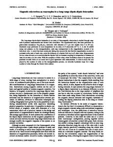
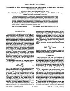
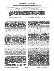
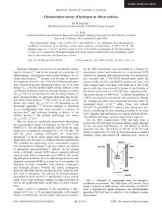
FIG. 3. Electric-field pattern of the TE mode 共electric field parallel to axis of the air columns兲 for the intersection of a dielectric slab waveguide and a PBG waveguide with equal slab thicknesses. The specifications of the waveguides are the same as those in Fig. 1. The normalized frequency of the source is a/(2 c)⫽0.258, which is out of the photonic bandgap of the photonic crystal.
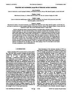
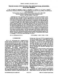
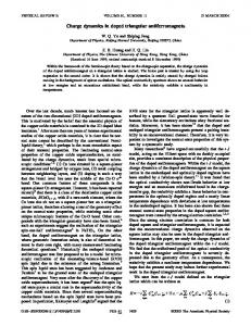
if these extended modes can couple to the guided mode, the PBG waveguide will become lossy, even though the condition for total internal reflection is still valid. Such extended cladding modes do not exist in a dielectric slab waveguide resulting in a wider frequency range for low-loss guiding. For the PBG waveguide analyzed here, this loss is negligible for a range of frequencies 关 0.204⬍ a/(2 c)⬍0.267兴 that is larger than the photonic bandgap 关 0.216⬍ a/(2 c) ⬍0.248兴 . As Fig. 2 suggests, the field pattern of the PBG waveguide mode is similar to that of the slab waveguide. Therefore, we expect very good coupling between the two waveguides over a relatively wide frequency range. Figure 3 shows the electric-field pattern of a TE mode 共electric field parallel to the axis of the air columns兲 at the intersection between a slab waveguide and a PBG waveguide with similar slab thicknesses and permittivities. The field patterns in Fig. 3 were calculated using a constant frequency Huygens source14 to excite the fundamental TE mode 共electric field normal to the calculation plane兲 in the slab waveguide at x ⫽x 0 . The frequency of the source used in this calculation was a/(2 c)⫽0.258, which is out of the bandgap. We chose the thickness of the slab 共d兲 small enough to obtain single mode propagation in both the PBG waveguide and the slab waveguide at this frequency. This is an important criterion for practical applications. The PBG waveguide mode at this frequency 共even though it is out of the photonic bandgap兲 has very low loss since it is well confined in the slab region. To calculate the transmission spectrum from the slab waveguide to the PBG waveguide, we used a pulsed Huygens source to excite the fundamental TE mode in the slab waveguide at x⫽x 0 in Fig. 3. We calculated the spectrum of the power transmitted through the PBG waveguide by taking the Fourier transform of the fields and then integrating the Poynting vector over a surface of 60 calculation cells centered at the middle of the PBG slab at x⫽x 1 in Fig. 3. The power transmission coefficient was then calculated as the ratio of the transmitted and incident powers. Figure 4 shows the power transmission coefficient 共from the slab waveguide to the PBG waveguide兲 versus frequency for the waveguide connection shown in Fig. 3. As Fig. 4 shows, it is possible to
FIG. 4. Spectrum of power transmission coefficient from a dielectric slab waveguide to a PBG waveguide with similar slab properties. The solid curve and the dotted curve show the power transmission coefficients for the cases where there is a GaAs or an air buffer layer on top and bottom of the PBG mirrors 共between the PBG mirrors and the PML兲, respectively. The thicknesses of both buffer layers are 10 calculation cells.
have a high transmission coefficient between a slab waveguide and a PBG waveguide over a relatively wide range of frequencies corresponding to the range of frequencies over which the PBG waveguide mode has very low loss. The minimum transmission at a/(2 c)⯝0.18 as well as the variations 共or ripples兲 of the transmission coefficient in the high transmission region, is due to the distributed Bragg reflection 共DBR兲 of the guiding mode from the periodic structures on the top and bottom of the slab region. The smaller transmission coefficient at the higher frequencies 关 a/(2 c)⬎0.28兴 is due to the excitation of other modes of the PBG structure that are lossy. These modes attenuate as they propagate along the PBG waveguide. As Fig. 4 shows, putting air instead of GaAs on top and bottom of the entire PBG waveguide 共between the PBG mirrors and the PML兲 will affect the smaller peak 关at a/(2 c)⯝0.295兴 in the transmission coefficient. Our calculation also showed that this smaller peak depends on the number of PBG layers used on the top and the bottom of the middle slab. However, the high transmission behavior at middle frequencies is not significantly influenced by either the number of PBG mirror layers or the material at the top and bottom of the structure. This is due to the fact that for these frequencies, the mode is well confined and is not influenced by the structure far from the slab region. Figure 5 shows the power transmission spectra from a slab waveguide to a PBG waveguide for two different PBG waveguide lengths 共10a and 20a兲. The high power transmission coefficient out of the bandgap for both cases is another indication of the guiding with low loss out of the bandgap, since the transmission coefficient of a lossy mode is reduced considerably by doubling the waveguide length. Note that the location of the minimum at a/(2 c)⯝0.18 is the same for both cases in Fig. 5, while the transmission spectrum to the longer waveguide has more ripples in the high transmission region. This can be explained by attributing the transmission minimum at a/(2 c)⯝0.18 to DBR. Our results suggest that the two important physical mechanisms for guiding light in PBG waveguides are 共1兲 total internal reflection 共due to the index contrast between
033308-3
BRIEF REPORTS
PHYSICAL REVIEW B 64 033308
FIG. 5. Spectra of power transmission coefficients from a dielectric slab waveguide to two PBG waveguides with lengths of 10a and 20a, respectively. The buffer layers on top and bottom of the PBG mirrors 共between the PBG mirrors and the PML兲 in both cases are assumed to be air.
middle slab and cladding兲 and 共2兲 distributed Bragg reflection 共due to the presence of the photonic crystal兲. Similar mechanisms are responsible for guiding in photonic-crystal fibers,15 which have a periodic array of holes. These photonic-crystal fibers come in two varieties: 共1兲 fibers whose symmetry has been broken by replacing the central hole with glass to create a high index defect, and 共2兲 fibers whose symmetry has been broken by replacing the central hole with a larger hole. In the former case, guiding is achieved by total internal reflection as the average index of the dielectric region with the holes 共the cladding region兲 is less than that in the central filled region 共or core region兲.16 Although the general guiding mechanisms in planar PBG waveguides and photonic-crystal fibers are similar, there are two major differences between the two types of waveguides. First, the plane of discrete periodicity of the two-dimensional photonic crystal is perpendicular to the guiding direction in photonic-crystal fibers while it includes the direction of propagation in planar PBG waveguides. In other words, planar PBG waveguides have discrete periodicity in the guiding direction while photonic-crystal fibers do not. As a result, DBR in the guiding direction is always present in PBG waveguides while it is not present in photonic-crystal fibers. The second difference between planar PBG waveguides and photonic-crystal fibers is the confinement of light in air-core structures. Light is well confined in the core of an air-core photonic-crystal fiber, since the plane of twodimensional periodicity of the photonic crystal is perpen-
E. Yablonovitch, Phys. Rev. Lett. 58, 2059 共1987兲. S. John, Phys. Rev. Lett. 58, 2486 共1987兲. 3 N. Stefanou and A. Modinos, Phys. Rev. B 57, 12 127 共1998兲. 4 A. Yariv et al., Opt. Lett. 24, 711 共1999兲. 5 A. Mekis et al., Phys. Rev. Lett. 77, 3787 共1996兲. 6 S. Lin et al., Science 282, 274 共1998兲. 7 T. Baba et al., Electron. Lett. 35, 654 共1999兲. 8 K. S. Yee, IEEE Trans. Antennas Propag. AP-14, 302 共1966兲. 9 C. T. Chan et al., Phys. Rev. B 51, 16 635 共1995兲.
dicular to the direction of propagation. On the other hand, the photonic crystal in a planar PBG waveguide can only help confine the light in one perpendicular direction 共compared to the guiding direction兲, since the plane of periodicity includes the propagation direction. In dielectric-core PBG waveguides, the confinement in the third direction is provided by total internal reflection. On the other hand, since air-core PBG waveguides have a low index core, there is no confinement by total internal reflection. This explains why previous experimental work in planar photonic-crystal optical waveguides has been performed using dielectric-core waveguides. Therefore, we limited our attention in this paper to dielectric-core photonic-crystal optical waveguides. The results of this paper prove the possibility of guiding in PBG waveguides out of the photonic bandgap. We believe that this fact must be considered in interpreting the experimental results regarding the PBG waveguides. In other words, we should not interpret any evidence of the guiding in PBG waveguides to the guiding modes inside the photonic bandgap. For example, some experimental results for the design of bends using photonic-crystal optical waveguides have been recently reported.7 The results of this paper suggest that the low experimental transmission through the bends in the reported experiments, could be due to the guided modes out of the photonic bandgap that are not efficiently transmitted in waveguide bends. In conclusion, we showed that there exist some guided modes in PBG waveguides outside the photonic bandgap. These modes are similar to the conventional slab waveguide modes, and are efficiently guided over a frequency range larger than the photonic bandgap. The properties of these modes are the results of total internal reflection and DBR from the periodic structure in the guiding direction. We also showed that we can obtain efficient power transmission from a slab waveguide to a PBG waveguide over a relatively wide frequency range. This is a very important result as it suggests that we can make optical elements using sections of PBG waveguides and using slab waveguides to efficiently connect different PBG optical elements. The results are significant in explaining the experimental results regarding PBG waveguides. The authors thank Mr. Gregory Steckman for helpful suggestions about the graphics of the paper. This work was supported in part by the Air Force Office of Scientific Research under Contract No. AFOSR-61557, and by the Office of Naval Research 共Y. S. Park兲.
J. P. Berenger, J. Comput. Phys. 114, 185 共1994兲. R. Meade et al., J. Appl. Phys. 75, 4753 共1994兲. 12 A. Mekis et al., Phys. Rev. B 58, 4809 共1998兲. 13 A. Adibi et al., Electron. Lett. 36, 1376 共2000兲. 14 D. E. Merewether et al., IEEE Trans. Nucl. Sci. NS-27, 1829 共1980兲. 15 J. C. Knight et al., J. Opt. Soc. Am. A 15, 748 共1998兲. 16 J. C. Knight et al., Science 282, 1476 共1998兲.
1
10
2
11
033308-4