PHYSICAL REVIEW B
VOLUME 60, NUMBER 11
15 SEPTEMBER 1999-I
Action spectra of the two-stage photoinduced insulator-metal transition in Pr1ⴚx Cax MnO3 M. Fiebig* Department of Applied Physics, The University of Tokyo, Tokyo 113-8656, Japan and Japan Science and Technology Corporation (JST), Tokyo 171-0031, Japan
K. Miyano and T. Satoh Department of Applied Physics, The University of Tokyo, Tokyo 113-8656, Japan
Y. Tomioka Joint Research Center for Atomic Technology (JRCAT), Tsukuba 305-0046, Japan
Y. Tokura Department of Applied Physics, The University of Tokyo, Tokyo 113-8656, Japan and Joint Research Center for Atomic Technology (JRCAT), Tsukuba 305-0046, Japan 共Received 6 November 1998; revised manuscript received 1 April 1999兲 The action spectra for the photoinduced insulator-metal transition in Pr1⫺x Cax MnO3 were investigated in the 0.45⫺3.05 eV range. The photon-density threshold for the transition exhibits a gaplike behavior at ⬃0.4 eV with anisotropic features, and it is insensitive to the degree of carrier doping x. A two-stage mechanism is proposed for the transition. In the first stage, photoexcited charge carriers melt down the charge-ordered state by screening effects, which is followed by a local formation of metastable metallic domains. In the second stage, the barrier between the metallic domains is overcome by an applied electric field resulting in a continuous conducting path that remains stable as long as the current is maintained. 关S0163-1829共99兲03935-1兴
I. INTRODUCTION
Perovskite manganites with the formula R 1⫺x A x MnO3 (R and A being rare- and alkaline-earth ions, respectively兲 are a model system for extensive testing of the concept of ‘‘phase control.’’ Charge, spin, orbital, and lattice act as independent yet strongly coupled physical degrees of freedom that can be influenced by a variation of the compositional degrees of freedom R, A, and x. The interplay is subtle and leads to highly complex phase diagrams and a number of unusual magnetic and electronic properties of these compounds.1–3 The most spectacular of these may be a change of resistivity of up to more than ten orders of magnitude in the course of an insulator-metal transition 共IMT兲 upon the application of a magnetic field, the so-called colossal magnetoresistance 共CMR兲.4 In the CMR compound Pr1⫺x Cax MnO3 , the small ionic radii of the cations at the A site lead to a small transfer integral between Mn ions. Charge localization is therefore strong, and the compound shows insulating behavior over the whole composition range. For 0.3⭐x⭐0.5, the material is charge ordered at low temperature, exhibiting a CE-type structure 关Fig. 1共b兲, inset兴, which is incommensurate for x ⫽0.5.5,6 The charge-ordered state is energetically nearly degenerate with the charge delocalized metallic state driven by the double-exchange mechanism. Therefore, a first-order phase transition from the insulating ‘‘charge lattice’’ into a conducting ‘‘charge liquid’’ can be induced when a critical magnetic field is exceeded.7 As the Mn4⫹ sites are replaced by Mn3⫹ ions, the charge transfer along the c axis is progressively promoted. The material thus undergoes the IMT at 0163-1829/99/60共11兲/7944共6兲/$15.00
PRB 60
a systematically lower magnetic field as the composition x varies from 0.5 to 0.3.8 The application of external forces other than a magnetic field can also lead to a breakdown of charge ordering and therefore an IMT.9–12 The photoinduced IMT 共Ref. 12兲 is outstanding in the sense that only a well-localized conducting path is generated whereas the bulk of the sample remains insulating. The phase transition is therefore distinctly localized.13 Not much is known about light induced phase transitions14 and, in particular, about the microscopic mechanism and its relation to the well-studied magnetic field induced IMT in our case. Here we report the action spectra of the photoinduced IMT, from which we propose that the transition proceeds in two distinct steps: creation of metallic domains by light followed by their fusion by the applied electric field. II. EXPERIMENTAL
Five different bulk samples of Pr1⫺x Cax MnO3 with x ⫽0.30, 0.35, 0.40, 0.45, and 0.50 and lateral dimensions of 1–4 mm were investigated. The x⫽0.40 sample was an orthorhombic single-domain single crystal whose a, b, and c axes had been determined by x-ray diffraction. In the other samples, the almost cubic symmetry of the crystal lattice led to a multi-domain structure of the principal axes. After applying the same polishing process to all the samples,4,12 some of them exhibited mirrorlike surfaces whereas others appeared blurred due to an infrequent pattern of microscopic defects. A pair of gold electrodes separated by a straight 25 m gap was vacuum evaporated onto the surface of the samples and connected to a dc regulating power supply pro7944
©1999 The American Physical Society
PRB 60
ACTION SPECTRA OF THE TWO-STAGE . . .
7945
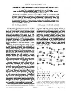
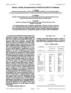
Once the conducting path has been formed, it remains stable without further illumination as long as a current is flowing between the electrodes, but the sample returns to the initial insulating state immediately after the current has been switched off. The path is always formed inside the illuminated region.13 Consequently, the phase transition is most easily induced if the laser spot is well focused and fully covers the space between the electrodes at an arbitrary position along the gap. Since the light-intensity threshold for the transition is highly sensitive even to tiny misalignments, great care had to be taken to achieve and maintain an optimal adjustment. For this purpose the image of the sample was monitored with a CCD camera equipped with a telephoto lens. This enabled the adjustment of the laser beam and helped to detect and avoid damages of the sample surface or the electrodes. Still, frequent fine alignment was required since wavelength tuning of the OPO led to defocusing and a beam walk off. The criterion for the best adjustment was minimization of the pulse energy required for the photoinduced IMT. Gradually occurring effects, due to the unstable performance of the OPO laser beam or to microscopic damages of the electrodes after recurrent induction of the phase transition, were taken into account by repeating the measurement several times during one experimental run. Asymmetries originating in an elliptical laser-beam profile were compensated by verifying the threshold for the IMT for selected photon energies with the sample rotated by 90°. FIG. 1. 共a兲 Spectral and polarization dependence of the photon density required to trigger the IMT in a Pr0.6Ca0.4MnO3 single crystal at 30 K for a voltage of 50 V applied to the sample electrodes separated by a 25 m gap. Circles and squares denote a transition induced by applying the voltage 共U兲 along the b or c axis of the crystal, respectively. Open and closed symbols denote a polarization of the incident light along the b or c axis of the crystal, respectively. The inset shows the spectral dependence of the anisotropy ratio (b)/ (c). 共b兲 Optical conductivity spectrum of the sample at 10 K for electric fields of the incident light (U opt) polarized along the b and c axis, respectively. The inset shows the collinear CE-type spin-, orbital-, and charge-ordering structure. Lobes denote the manganese d 3x 2 ⫺r 2 and d 3y 2 ⫺r 2 orbitals.
tected by a 500-⍀ resistance. On the x⫽0.4 single-domain sample, two pairs of electrodes with gaps perpendicular to each other were evaporated so that the electric field could be applied along the b and c axes simultaneously with independent power supplies. The samples were mounted in a continuous-flow helium cryostat and kept at a temperature of 30 K unless otherwise stated. As light source, an optical parametric oscillator 共OPO兲 pumped by the third harmonic of a Nd:YAG laser was used. The IMT was induced by illuminating the gap between the electrodes with 5 ns light pulses from the OPO at a photon energy of 0.45⫺3.05 eV, while applying a fixed voltage of up to 50 V to the electrodes. The transition was noted as a sudden drop of the resistance between the electrodes after a single light pulse.12 The polarization and intensity of the light pulses were controlled with three revolving Glan-Thompson prisms. The pulse energy was monitored with a flat-response Joule meter, and the beam diameter was measured with a traveling knife edge. The absorbed photon density was calculated using results of these measurements and was corrected for the reflectivity.
III. RESULTS AND DISCUSSION
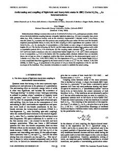
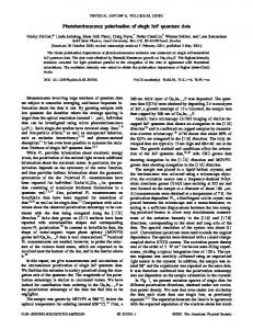
Figure 1共a兲 shows the action spectrum, that is, the spectral and polarization dependence of the minimum photon density required to trigger the IMT in the Pr0.6Ca0.4MnO3 single crystal with 50 V applied. Since does not vary much at photon energies E⬎1.0 eV, only the low-energy range is shown in Fig. 1共a兲. There is distinct evidence for an energy gap at E⬃0.4 eV. The threshold density remains independent of the polarization of the incident light, but below E ⫽1.0 eV an anisotropy appears with respect to the direction of the applied electric field, the anisotropy ratio (b)/ (c) being shown in the inset in Fig. 1共a兲. For comparison, Fig. 1共b兲 shows the optical conductivity spectrum for light polarized along the b and c axis, respectively.15 Contrary to the action spectrum, the optical conductivity starts to rise at lower energy with a clear anisotropy with respect to the polarization of the incident light. Figure 2 shows the action spectra of all samples with 50 V applied to the electrodes. The x⫽0.40 spectrum of Fig. 2 was derived by averaging over the four spectra of Fig. 1共a兲. Since all other samples were not single domain, the directional dependence of their spectra was not studied. For E ⬎2.0 eV, saturates at a value quite insensitive to both photon energy and carrier doping. By averaging over the five different curves, the saturated photon density is found to be sat⫽(24.6⫾2.9)⫻1015 cm⫺2 in the 2.0–3.0 eV energy range 共inset in Fig. 2兲. For E⬍2.0 eV, increases with decreasing photon energy. A steep increase of at the lowest photon energies indicates the presence of an energy gap at E⬃0.4 eV. At 0.45 eV, is about 50 times larger than sat with a variation of ⫾50% for the different samples. The variation, however, does not systematically depend on the degree of carrier doping x. It is rather due to the aforementioned differences in sample quality or long-term variations of the laser performance. Nonetheless, the anisotropy
7946
FIEBIG, MIYANO, SATOH, TOMIOKA, AND TOKURA
PRB 60
FIG. 2. Spectral dependence of the photon density required to trigger the IMT in Pr1⫺x Cax MnO3 at 30 K for a voltage of 50 V applied to the sample electrodes separated by a 25 m gap. The inset shows the high-energy range of the spectrum averaged over all five samples and a linear fit to the data 共line兲.
关 (b)/ (c)⬃1.5 at E⫽0.45 eV] for the x⫽0.4 sample 关Fig.1共a兲兴 is reliable, since the data were gained from a single sample and in a single run. The insensitivity to the degree of carrier doping of the spectra shown in Fig. 2 is the most remarkable feature. As shown in Ref. 7 and mentioned earlier, it becomes easier to induce the IMT in a magnetic field upon a decrease from x ⫽0.5 to x⫽0.3. The absence of this tendency in our experiments shows that the mechanism underlying the photoinduced IMT acts on the charge-ordered state in a completely different way. The magnetic-field induced IMT described in Sec. I is an equilibrium process. The insulating state with low transfer integral at zero field and the metallic state with higher transfer integral at a nonzero field are about degenerate, and the Zeeman energy simply biases the fluctuations around the system equilibrium to find a path from the insulating to the metallic ground state. In this sense, the transition is governed by the weakest path through phase space between the two ground states. The optical transition, on the other hand, is a nonequilibrium process and may be divided into steps as follows: 共1兲 From the localized state, charge carriers are excited across the Mn3⫹ →Mn4⫹ charge-transfer gap by a light pulse. 共2兲 Due to screening by the delocalized electrons, the chargeordered state melts, and 共3兲 the formation of a multidomain metallic phase occurs instead. 共4兲 The decay of this metastable state is interrupted by the electric field by fusing the domains into a continuous conducting path between the electrodes. Once the path is established, the dc current provides the screening and maintains the metallic phase for an infinite time. 共1兲 The relevant optical excitation process in this model can be seen by comparing Figs. 1共a兲 and 1共b兲. The lowenergy tail in the optical conductivity for the c-polarized light is due to the extended one-dimensional electronic state along the c axis mediated by the partial filling of the e g orbitals at Mn4⫹ sites as discussed before. The optical excitation within this extended state, however, does not disrupt the charge-ordering pattern and hence cannot lead to the metallic state, which must be three-dimensional.15 Clearly,
the photoexcitation has to overcome the highest barrier in all directions against charge delocalization for the photoinduced IMT. This should be the charge-transfer excitation from Mn3⫹ to Mn4⫹ in the CE-type charge- and orbitalordered state. The insensitivity of the gap energy and of to the composition x is reasonable since the CE-type ordering, which is overcome by the photoinduced screening, persists throughout the entire composition range 0.3⭐x ⭐0.5.6 共2兲 Phase transition due to screening by photoinduced charge carriers are known in ferroelectric materials where screening modifies the frequency of the soft polarization vibration mode and therefore the Curie temperature.16 As to the manganite compounds, screening attenuates the longrange Coulomb interaction, which, besides Jahn-Teller and other local lattice distortions, is responsible for the charge localization.17,18 The Hamiltonian for the double-exchange interaction is modified by the screening to a much lesser extent.19 When the screening is strong enough, the charge localization therefore becomes inferior to the double exchange, and the IMT occurs. 共3兲 The photoinduced metallic phase is created locally and therefore strongly competes with the surrounding antiferromagnetic phase.20 Due to this ‘‘pressure,’’ the metallic state is not stable, even though it is surprisingly long lived with a lifetime of about 1 s.21,22 If the sample has fully undergone the IMT in a magnetic field, the lifetime is greatly extended23 due to the absence of the background pressure so that the metallic state is regarded as stable. Note that the described photoexcitation is a quantum process. Therefore, its quantum efficiency saturates at high photon energies 共Fig. 2, inset兲. On the other hand, the power efficiency goes down as the photon energy goes up, disproving that laser heating is of any significance.12,13,25 共4兲 It is known that the photoinduced phase is ferromagnetic.24 In the absence of the external magnetic field, however, the ferromagnetic domains are randomly oriented and cannot easily merge. The role of the external electric field in the photoinduced IMT is to fuse the domains and to form a continuous conducting path between the electrodes, which prevents the charge carriers from relocalization as
PRB 60
ACTION SPECTRA OF THE TWO-STAGE . . .
7947
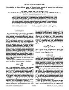
FIG. 3. Voltage dependence of the photon density required to trigger the IMT in Pr0.6Ca0.4MnO3 at 30 K. The threshold values (U) were normalized to (50 V) and averaged over six different photon energies (E⫽0.5, 0.6, 0.7, 0.9, 1.2, and 1.6 eV兲. The electric field was applied along 共a兲 the b axis or 共b兲 the c axis of the sample, respectively.
long as the current is maintained through it. The fusing process requires essentially the electrical breakdown in the insulating parts between the domains. Creation of metastable metallic domains by light followed by their fusion into a stable metallic path by the applied voltage constitute our two-stage photoinduced IMT model. The above scenario is buttressed by the observation that the resistance of the conducting path 共see below兲 is independent of the degree of carrier doping whereas the ohmic resistance of the samples in the insulating state changes by three orders of magnitude while going from x⫽0.5 to x ⫽0.3.25 The threshold thus reflects the resistive properties of the metallic state, which corroborates that is determined by the electric field applied to the sample in the state after the laser irradiation when the metallic state is already present. The two-stage model is also supported by Fig. 3, in which the threshold photon density is plotted as a function of the applied voltage. The threshold values at six different photon energies (E⫽0.5, 0.6, 0.7, 0.9, 1.2, and 1.6 eV兲 for the electric field applied along the b or c axis of the x⫽0.4 sample, respectively, were normalized to the threshold at U ⫽50 V and averaged over all six energies to arrive at 具 norm(U) 典 ⫽ 具 (U)/ (50 V)典. The small 5% variance of
the averaged value and the insensitivity to the direction of the applied electric field confirm that norm(U) is independent of both E and of the orientation of the crystal. According to the two-stage model, the voltage required to trigger the generation of the conducting path should only depend on the density of metallic domains, irrespective of the photon energy of the excitation. Even though the required photon density depends on E 共because the density of metallic domains does兲, the normalized threshold value norm(U) should not, and indeed it does not. Let us further note two distinct features in Fig. 3. The first is the linear relationship between the reciprocal normalized threshold and the applied voltage, and the second is the 5 V offset at the abscissa. Both cannot be understood in terms of simple percolation26 or Ostwald ripening phenomena.27 In either case, more photons create more metallic domains, which at some point should fill up the space between the electrodes resulting in the metallic path at zero applied voltage. One would expect an abrupt drop of applied voltage as 1/ norm approaches zero, and a nonzero intercept on the ordinate rather than on the abscissa. The behavior shown in Fig. 3 can be understood if we consider the internal degree of
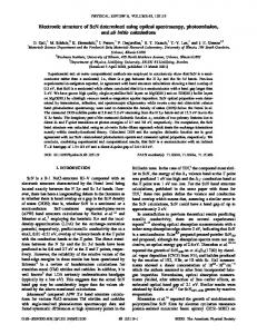
˜ across the conducting FIG. 4. Voltage drop U path as a function of the current flowing through it along the b or c axis of the x⫽0.4 sample, respectively. Temperature is 30 K. The inset ˜ (b)/U ˜ (c). shows the ratio U
7948
FIEBIG, MIYANO, SATOH, TOMIOKA, AND TOKURA
PRB 60
FIG. 5. Temperature dependence of the photon density required to trigger the IMT in a Pr0.6Ca0.4MnO3 single crystal with light at 1.2 eV for a voltage of 30 V applied to the sample electrodes separated by a 25 m gap. The dashed line marks the temperature above which the material becomes instable against the electric-field induced IMT.
freedom of the metallic domains, the magnetization. Because the total magnetization should be conserved during the photoexcitation, the domains that appear out of the antiferromagnetic background must be accompanied by domains with opposite spin, the boundary being the antiferromagnetic insulating wall. This is not to be confused with a domain wall in an ordinary ferromagnetic metal. Even at the limit of infinite light intensity, the boundary between the domains is left. The applied field is needed to overcome this boundary whereby the 5 V offset must be exceeded in order to maintain the continuous metallic path in accordance with Fig. 4. With the above view, the anisotropy in Fig. 1共a兲 can be easily understood in terms of the aforementioned ‘‘pressure.’’ One signature of such an effect is the current-voltage ˜ ) relationship after the IMT, which is shown in Fig. 4. (I-U ˜ /I represents the ‘‘stress’’ needed to mainThe resistance U tain the metallic path against the surrounding antiferromagnetic state. With the width of the conducting path corre˜ curve shows strong sponding to the path current, the I-U ˜ negative differential resistance dU /dI.25,28 According to Fig. 4, the resistance for a given current along the b axis is 50% higher than for the c axis. This reveals a corresponding anisotropy of the background pressure which in turn explains the anisotropy of with respect to the direction of the electric field in Fig. 1共a兲. The final evidence that the photoinduced IMT occurs far away from the thermal equilibrium and that it is not affected by laser heating is presented in Fig. 5, in which is plotted as a function of the temperature. The incident photon energy and the applied voltage were fixed at 1.2 eV and 30 V, respectively. The insensitivity of the photoinduced IMT to the temperature below 53 K is obvious. Above 53 K, the material becomes unstable against the electric-field induced IMT 共Ref. 9兲 so that the phase transition already occurs in the absence of laser irradiation. If the underlying mechanisms for the two types of IMT’s were related to each other, their
effects would add up, and should smoothly decrease towards zero at 53 K. Lack of such a behavior indicates that the role of the applied field in the respective IMT’s is completely different. IV. CONCLUSION
In summary, the application of optical spectroscopy revealed that the photoinduced IMT in Pr1⫺x Cax MnO3 can be regarded as a process with two largely independent stages. At the first stage, charge carriers are photoinduced in a charge-transfer excitation. The screening effect weakens the strong correlation between the electrons leading to the reorganization of the local electronic structure from that of the charge-ordered insulator to that of the metallic phase. At the second stage, the insulating barriers between the isolated metallic domains are overcome by an applied electric field, and a metallic path is formed between the electrodes. Unlike the magnetic-field induced IMT, which works via the amplification of double exchange, the photoinduced IMT works via the attenuation of charge ordering. It is therefore insensitive to the degree of carrier doping. According to the proposed model, the presence of the metallic state is due to photoexcitation whereas the external electric field enables its persistency. Hence, evidence for the metallic state should be found in a pump-and-probe experiment in which the spectral change of reflectivity accompanying the phase transition is probed in the absence of an electric field. An investigation of the temporal evolution of the photoinduced IMT would therefore offer a different approach to the problem of ‘‘phase control.’’ ACKNOWLEDGMENTS
This work was supported by the Grant-in-Aid for COE research. The work at JRCAT was supported by NEDO. The work of M.F. was supported by the CREST project of JST.
PRB 60
ACTION SPECTRA OF THE TWO-STAGE . . .
*Author to whom correspondence should be addressed. Electronic address:
[email protected] 1 A. J. Millis, Nature 共London兲 392, 147 共1998兲. 2 Y. Tokura, Curr. Opin. Solid State Mater. Sci. 3, 175 共1998兲. 3 H. Kuwahara and Y. Tokura, in Giant Magnetoresistance and Related Properties of Metal Oxides, edited by C. N. R. Rao and B. Raveau 共World Scientific, Singapore, in press兲. 4 Y. Tomioka, A. Asamitsu, Y. Moritomo, and Y. Tokura, J. Phys. Soc. Jpn. 64, 3626 共1995兲. 5 Z. Jirak, S. Krupicka, Z. Simsa, M. Dlouha, and S. Vratislav, J. Magn. Magn. Mater. 53, 143 共1985兲. 6 H. Yoshizawa, H. Kawano, Y. Tomioka, and Y. Tokura, Phys. Rev. B 52, R13 145 共1995兲; J. Phys. Soc. Jpn. 65, 1043 共1996兲. 7 Y. Tomioka, A. Asamitsu, H. Kuwahara, Y. Moritomo, and Y. Tokura, Phys. Rev. B 53, R1689 共1996兲; Y. Tomioka, A. Asamitsu, Y. Moritomo, and Y. Tokura, J. Phys. Soc. Jpn. 64, 3626 共1995兲. 8 M. Tokunaga, N. Miura, Y. Tomioka, and Y. Tokura, Phys. Rev. B 57, 5259 共1998兲. 9 A. Asamitsu, Y. Tomioka, H. Kuwahara, and Y. Tokura, Nature 共London兲 388, 50 共1997兲. 10 Y. Moritomo, H. Kuwahara, Y. Tomioka, and Y. Tokura, Phys. Rev. B 55, 7549 共1997兲. 11 V. Kiryukhin, D. Casa, J. P. Hill, B. Keimer, A. Vigliante, Y. Tomioka, and Y. Tokura, Nature 共London兲 386, 813 共1997兲. 12 K. Miyano, T. Tanaka, Y. Tomioka, and Y. Tokura, Phys. Rev. Lett. 78, 4257 共1997兲. 13 M. Fiebig, K. Miyano, Y. Tomioka, and Y. Tokura, Science 280, 1925 共1998兲. 14 Relaxation of Excited States and Photoinduced Phase Transi-
7949
tions, edited by K. Nasu, Springer Series in Solid State Sciences Vol. 124 共Springer-Verlag, Berlin, 1996兲. 15 Y. Okimoto, Y. Tomioka, Y. Onose, Y. Otsuka, and Y. Tokura, Phys. Rev. B 57, R9377 共1998兲. 16 V. M. Fridkin, Photoferroelectrics Springer Series in Solid State Sciences Vol. 9, 共Springer-Verlag, Berlin, 1979兲, p. 61ff. 17 V. I. Anisimov, I. S. Elfimov, M. A. Korotin, and K. Terakura, Phys. Rev. B 55, 15 494 共1997兲. 18 A. J. Millis, R. Mueller, and B. Shraiman, Phys. Rev. B 54, 5405 共1996兲. 19 S. Ishihara, J. Inoue, and S. Maekawa, Phys. Rev. B 55, 8280 共1997兲. 20 M. Fiebig, K. Miyano, Y. Tomioka, and Y. Tokura, Appl. Phys. Lett. 74, 2310 共1999兲. 21 K. Ogawa and K. Miyano 共unpublished兲. 22 M. Fiebig, K. Miyano, Y. Tomioka, and Y. Tokura 共unpublished兲. 23 A. Anane, J. P. Renard, L. Reversat, C. Dupas, P. Veillet, M. Viret, L. Pinsard, and A. Revcolevschi, Phys. Rev. B 59, 77 共1999兲. 24 Y. Okimoto, Y. Tokura, Y. Tomioka, Y. Onose, Y. Otsuka, and K. Miyano, Mol. Cryst. Liq. Cryst. Sci. Technol., Sect. A 315, 257 共1998兲. 25 K. Ogawa, W. Wei, K. Miyano, Y. Tomioka, and Y. Tokura, Phys. Rev. B 57, R15 033 共1998兲. 26 D. Stauffer, Introduction to Percolation Theory 共Taylor & Francis, London, 1985兲. 27 B. Lewis and J. C. Anderson, Nucleation of Thin Films 共Academic, New York, 1978兲. 28 T. Mori, K. Ogawa, K. Yoshida, K. Miyano, Y. Tomioka, and Y. Tokura, J. Phys. Soc. Jpn. 66, 3570 共1997兲.