sparse output of the DVS, traditional computer vision al- ... through the NCCR Robotics, Samsung Electronics Corporation, ETH Zurich, .... The readout building blocks: The top/right edges of the array are used for the asynchronous DVS ...
IEEE JOURNAL OF SOLID-STATE CIRCUITS, VOL. 49, NO. 10, OCTOBER 2014
2333
A 240 × 180 130 dB 3 µs Latency Global Shutter Spatiotemporal Vision Sensor Christian Brandli, Student Member, IEEE, Raphael Berner, Member, IEEE, Minhao Yang, Student Member, IEEE, Shih-Chii Liu, Senior Member, IEEE, and Tobi Delbruck, Fellow, IEEE
Abstract—Event-based dynamic vision sensors (DVSs) asynchronously report log intensity changes. Their high dynamic range, sub-ms latency and sparse output make them useful in applications such as robotics and real-time tracking. However they discard absolute intensity information which is useful for object recognition and classification. This paper presents a dynamic and active pixel vision sensor (DAVIS) which addresses this deficiency by outputting asynchronous DVS events and synchronous global shutter frames concurrently. The active pixel sensor (APS) circuits and the DVS circuits within a pixel share a single photodiode. Measurements from a 240×180 sensor array of 18.5 µm2 pixels fabricated in a 0.18 µm 6M1P CMOS image sensor (CIS) technology show a dynamic range of 130 dB with 11% contrast detection threshold, minimum 3 µs latency, and 3.5% contrast matching for the DVS pathway; and a 51 dB dynamic range with 0.5% FPN for the APS readout. Index Terms—Active pixel sensor (APS), address event representation (AER), CMOS image sensor, dynamic and active pixel vision sensor (DAVIS), dynamic vision sensor (DVS), event-based, neuromorphic engineering, spike-based.
I. INTRODUCTION
F
RAME-BASED image sensors are widely used in machine vision, but they suffer from a high power consumption and long data-processing delay. The event-driven dynamic vision sensor (DVS) [1]–[5] reduces redundant data for postprocessing by only reporting changes in scene reflectance with latencies and temporal precision down to microseconds. These features, along with the wide dynamic range ( 100 dB) of the DVS, makes these sensors particularly suitable for robotics [6], [7] and real-time tracking [8], where they can reduce systemlevel power consumption by a factor of 100 in comparison to conventional image sensors. Despite the efficiency of data processing by virtue of the sparse output of the DVS, traditional computer vision algorithms cannot be readily applied because no static scene information is encoded. To capture static light intensity, the ATIS sensor [4] uses the DVS pixel as an event trigger and Manuscript received November 25, 2013; revised March 31, 2014, and May 12, 2014; accepted July 01, 2014. Date of publication September 02, 2014; date of current version September 22, 2014. This paper was approved by Associate Editor Hideto Hidaka. This work was supported by the European Union funded project SeeBetter (FP7-ICT-2009-6), the Swiss National Science Foundation through the NCCR Robotics, Samsung Electronics Corporation, ETH Zurich, and the University of Zurich. C. Brandli, M. Yang, S.-C. Liu, and T. Delbruck are with the Institute of Neuroinformatics, University of Zurich and ETH Zurich, 8057 Zurich, Switzerland. R. Berner is with Abilis Systems, 1228 Plan-Les-Ouates, Switzerland. Color versions of one or more of the figures in this paper are available online at http://ieeexplore.ieee.org. Digital Object Identifier 10.1109/JSSC.2014.2342715
asynchronously updates the pixel intensity value based on pulse width modulation (PWM). However, this time-based intensity readout has three drawbacks: The use of an additional photodiode and complex intensity readout circuit makes the area of an ATIS pixel twice as large as a DVS pixel, the PWM intensity readout triples the asynchronous event data, and the non-uniform exposure can result in strong motion artifacts. To elaborate the last point in an example, a dark, narrow moving object can become invisible in the ATIS intensity readout because intensity measurements are repeatedly reset before completion due to consecutively incoming event triggers with short intervals. In conventional CIS, motion artifacts can be minimized by using a global shutter. The proposed “dynamic and active pixel vision sensor—DAVIS” (formerly called apsDVS [9], [10]) combines the DVS with an active pixel sensor (APS) at the pixel level. It allows simultaneous output of asynchronous events and synchronous frames. Even though the two readout circuits share the same photodiode, they can operate independently. The SBRet10 chip [9], the first generation of the DAVIS, produces motion artifacts because it uses a rolling shutter scheme [10]. The improved DAVIS design implemented in the SBRet20 chip presented in this paper resolves this problem for it allows global shutter operation. Global shutter image sensors are often used in machine vision applications because minimal motion artifacts are necessary. The combined static and dynamic output of the DAVIS makes it promising in a range of applications: The DVS output can be used to track and segment fast moving objects, while the APS output allows for the recognition and classification of these objects using established machine vision techniques. Because tracking is done using only DVS events, the frame rate of the APS output can be set arbitrarily low. The combined advantage of the dual outputs makes the DAVIS sensor well-suited for mobile applications or distributed sensor networks with a tight power budget, because it allows low latency at low system-level power consumption. The rest of this paper is organized as follows. Section II explains the DAVIS concept, Section III describes the pixel design, Section IV describes the chip implementation, Section V presents characterization results and Section VI concludes the paper. II. DAVIS CONCEPT A useful property of the DVS pixel is that it does not consume the photocurrent during its operation and so the absolute
0018-9200 © 2014 IEEE. Translations and content mining are permitted for academic research only. Personal use is also permitted, but republication/ redistribution requires IEEE permission. See http://www.ieee.org/publications_standards/publications/rights/index.html for more information.
2334
IEEE JOURNAL OF SOLID-STATE CIRCUITS, VOL. 49, NO. 10, OCTOBER 2014
Fig. 1. DAVIS pixel schematic. The transistor-level schematic of the DVS is described in [1]. Caps represents the gate capacitance of MN2.
light intensity can be measured by integration of this current, as is done in conventional CIS. In the proposed DAVIS pixel, the intensity readout uses an active pixel readout scheme which is the most common readout scheme for CIS. The only major disadvantage of the APS readout is the limited intra-scene dynamic range, requiring an intelligent exposure control strategy. On the other hand this way of measuring the intensity has several advantages compared to the event-triggered approach used by the ATIS. The shared photodiode and the small size of the APS circuit lead to a pixel area that is only 5% larger than a DVS only pixel. The frames have a uniform exposure and they are acquired using a synchronous global shutter which makes them compatible with existing machine vision algorithms and applications. The sampling rate and the region of interest (ROI) can be chosen according to the demands of applications and the readout is independent of DVS activities. III. PIXEL DESIGN A. Fusion of the APS and DVS Pixel Design The pixel schematic (Fig. 1) shows how a simultaneous operation of the temporal contrast detection and the frame-based intensity readout is achieved without interfering with each other. The DVS photoreceptor circuit (MN6/MN7/MP1) holds the photodiode PD at virtual ground and the photocurrent which is available at the drain of MN6 allows the 4T APS [11] intensity readout with transistors MN1 to MN4. The cascode transistor MN5 protects the drain of MN6 from the large reset transient of Vdr. The APS signal is integrated on the parasitic gate capacitance Caps. To prevent saturated pixels from affecting the DVS pathway during integration, column reset CR is set to an intermediate overflow protection voltage level Vov of around 1.5 V instead of ground, which ensures that MN5 always stays in saturation. The DVS part of the pixel is similar to [1]: The photocurrent is continuously and logarithmically encoded by the photoreceptor output voltage Vpr at the gate of MN6. A source follower buffer isolates Vpr from the self-timed switched-capacitor amplifier, which amplifies the change from the last reset-level with a gain of 20. This amplified change is compared against ON and OFF thresholds by two common-source static inverter comparators
with different bias voltages on the static load transistor gates. As soon as one of the thresholds is crossed, an event is communicated to the periphery (ON for increasing intensity, OFF for decreasing intensity) and concurrently the switched-capacitor amplifier is reset by a pulse generated by the AER Logic block. This reset stores the new illumination level. Each output event thus encodes a fixed amount of change in log intensity since the last event. B. Comparison to Other Designs The DAVIS uses a logarithmic transimpedance photoreceptor circuit [1] where the photocurrent is sourced from the n-FET MN6 whose gate is driven by feedback; this will be called an n-FET photoreceptor. An alternative arrangement used by [2] sources the photocurrent from a p-FET whose source is driven by feedback, while the gate is held at a common voltage; this will be called a common-gate photoreceptor. Both circuits use a high gain inverting forward amplifier (MN7/MP1 in the DAVIS pixel). The common-gate photoreceptor reduces the Miller-capacitance of the circuit and thus improves the speed of the pixel. However it has two disadvantages: Firstly the photoreceptor forward amplifier bias current Ipr must be at least as large as the photo-current, which makes it harder to limit the pixel bandwidth. This capability is sometimes required to filter out flickering light sources or reduce noise. Secondly the common-gate photoreceptor prevents direct access to the photocurrent because it is sourced from the forward amplifier, rather than directly available at the drain of the feedback transistor MN6. Therefore a shared photodiode for an APS-DVS circuit is not possible with a common-gate photoreceptor. Although a current mirror allows copying the photocurrent (which is used in [2] for global gain control), this copied current would be too imprecise for an acceptable APS output. A practical problem with the nFET photoreceptor, which was observed in earlier unpublished designs where MN6 and MN7 were transistors with normal threshold voltage, can arise when the photocurrent is so small that the Vgs of MN6 becomes negative. This condition leads to decreased gain of the MN7-MP1 amplifier because MN7 might enter the linear region. This decreased gain decreases the photoreceptor bandwidth. In both
BRANDLI et al.: A 240×180 130 dB 3 µs LATENCY GLOBAL SHUTTER SPATIOTEMPORAL VISION SENSOR
2335
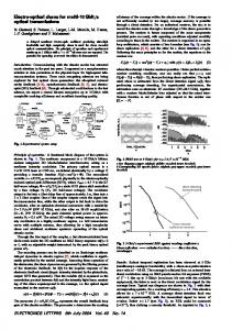
Fig. 2. The readout building blocks: The top/right edges of the array are used for the asynchronous DVS readout and the bottom/left edges for the shift-register pixel selection are used in the APS readout.
SBRet10 and SBRet20, MN6 and MN7 were replaced by highthreshold thick-gate transistors, as illustrated in Fig. 1. Measurements from a test pixel show that even in the dark, the Vpr is still high enough to ensure the saturation of MN7. In the ATIS [4] all the analog parts of the pixel are built with a 3.3 V power supply, requiring large n-well design rules for p-FETs. In the DAVIS sensor, this problem is addressed by running the DVS part of the pixel with 1.8 V supply. Because the APS part of the pixel consists of only n-FETs with no 3.3 V n-well, a compact design is achieved by using only the 1.8 V n-well design rules for the p-FETs in the DVS circuit. IV. SENSOR DESIGN This section discusses the communication interface for DVS events, the acquisition process of intensity images as well as pixel layout considerations. A. DVS Readout Design The DVS events are communicated using word-serial burst mode address-event representation (AER) circuits which are adapted from [12]. The circuits work as follows (block diagram in Fig. 2): If a pixel crosses threshold, it generates a request to transmit an event by pulling down a row request line which is shared by all pixels in a row (RR in Fig. 1). A fair arbitration circuit [13] chooses among all active requesting rows and
acknowledges a single one (RA). In this acknowledged row, all pixels that have crossed threshold then request in the column direction; the polarity of the event is encoded by different request lines (CRON for ON events, CROFF for OFF events). In the meantime, the row address is registered and transmitted off-chip. During the time ( 100 ns) it takes to transmit the row address, the column requests of the pixels in the acknowledged row are latched by an asynchronous state machine at the top of each column. A simplified arbitration tree sequentially registers, acknowledges (CA) and transmits all addresses of the requesting columns starting from the leftmost requesting column. If several pixels in a row make a request at the same time, their common row address will be transmitted only once. This scheme increases the communication bandwidth when compared to the bandwidth of transmitting a row and column address for every active pixel. All events in such a burst are treated as being simultaneous. (Even if these within-row events were individually time-stamped, they would probably not be resolved given that the digital timestamp resolution at the camera level is 1 us and that each event requires about 80 ns to be transmitted to the USB device controller.) B. APS Readout Design For the APS readout, differential double sampling is essential to remove significant FPN mainly caused by MN2. The first
2336
IEEE JOURNAL OF SOLID-STATE CIRCUITS, VOL. 49, NO. 10, OCTOBER 2014
Fig. 4. Global shutter APS timing diagram.
Fig. 3. Rolling shutter vs. global shutter DAVIS readout: Space-time view of the DVS events and the APS frames originating from a fan rotating at 50 Hz. (a) and (b) show the data in space-time. The APS sample readouts are visible as tilted planes. The DVS events and APS samples are dots. The newer events are colored red, the older ones green. The exposure time is shown by the yellow rectangle labeled “exposure”. (c) Output of rolling shutter and (d) global shutter readout.
sample is the reset voltage of the pixel and the second sample is the voltage at the end of the exposure period. The rolling shutter DAVIS readout uses a shift register along the x-axis that carries two bit patterns. These patterns are decoded by column-parallel logic. Using these bit patterns simplifies the interface because it requires only a single clock and data input. The first of these two bit patterns selects the column which is reset and sampled. The second bit pattern selects the column which is read out. This separation of the reset and signal columns allows a sequential readout of the two values in different columns. The distance between the two columns corresponds to the time between the reset read and signal read signals i.e., the exposure time. The first generation SBRet10 chip [9] is only capable of rolling shutter readout. The SBRet20 sensor reported here has both rolling and global shutter readout modes, which will be explained in the next paragraph. Fig. 3 compares images of a fan captured from SBRet20 in rolling and global shutter modes to show how the motion artifacts resulting from rolling shutter readout are eliminated by global shutter readout. In Fig. 3(a), the rolling shutter exposure corresponds to the distance between the reset and signal readout planes (marked as exposure). Because the columns are exposed at different times, the exposure plane is tilted and strong motion artifacts can be observed for fast moving objects, as seen by the highly distorted fan shape in Fig. 3(c). To allow a synchronous global exposure and to still maintain the differential double sampling, a globally-controlled switch TX (MN3) is added to the pixel from SBRet10 and the pixel APS reset signal CR is made globally and column-wise controllable. The global shutter readout timing diagram is shown in Fig. 4. To start the frame read, the integration capacitance
(Caps) is charged by setting and resulting in a soft reset of Vaps. This reset voltage is sampled by disconnecting TX and then reading out Vaps (“reset read”) by addressing the pixels using the APS readout shift registers. During the reset read, TX is set to 0 V and CR to Vov, the overflow protection level. After the reset level of the array is read out, the exposure starts by setting (“exposure”). By following this timing sequence, no charge is injected from Vdd into the already sampled reset voltage on Caps. The photocurrent is integrated on the capacitor Caps, which is about 5 times smaller than the PD capacitance in the DAVIS pixel. After the exposure time, the signal value is first sampled by disconnecting TX, which stores the exposure value at Vaps, and then Vaps is read out (“signal read”), and off-chip it is digitally subtracted from the reset level. The reset read and the signal read planes are separated as seen in Fig. 3(b): The TX switch is only connected during the global exposure for all the pixels (shown as the yellow exposure plane in Fig. 3(b)). This readout scheme leads to much weaker motion artifacts consisting of blurred edges along the direction of motion (Fig. 3(d)). The global shutter readout has the additional potential benefit of separating the readout and exposure phases, which could allow a region of interest (ROI) readout. An exposure can be started and stopped at any time, e.g., based on DVS activity. The signal readout could then also be sped up by reading out only part of the array if deemed useful. This partial readout is possible because of the separate exposure and readout phases enabled by the global shutter operation. In a rolling shutter readout, the TX switch is always on. After a column reset, all the reset values are read from the column. After this, the column reset CR is set to and the pixels of this column start to integrate. Because both the reset and integrated signal levels are read in the same frame, the kTC reset noise of the reset level is cancelled by the correlated difference between the reset and signal levels. The global shutter readout stores two samples on the Vaps node by using the TX switch, one for the reset sample and the other for the signal sample. Thus the global shutter differential double sampling
BRANDLI et al.: A 240×180 130 dB 3 µs LATENCY GLOBAL SHUTTER SPATIOTEMPORAL VISION SENSOR
2337
readout has the disadvantage of additional kTC sampling noise compared with the correlated double sampling rolling shutter readout. C. Layout and Process The SBRet20 DAVIS chip was built in a 180 nm 6M1P CMOS image sensor (CIS) process with MiM capacitors and uses surface photodiodes available in this CIS process, rather than the n-well photodiodes used in the standard mixed-signal process used for fabricating SBRet10 [9]. The CIS process used for SBRet20 has several additional potential advantages that have not yet been utilized including micro lenses, anti-reflection coating, and annealing steps that reduce junction leakage currents. They will be included in a future implementation. Fig. 5(a) shows a microphotograph of the 5 mm 5 mm die with an inlay of a 2 2 pixel layout. The pixel layout uses a quad-mirrored form to share source contacts and bias lines, and to group analog and digital parts of adjoining pixels [1]. It is essential to minimize parasitic capacitive coupling in the pixel layout, particularly to the high-impedance node PR. Parasitic capacitance extraction tools were used to identify and minimize these capacitances and were successful except for one capacitance as will be discussed in Section V-E. The pixel pitch is 18.5 m and the fill factor is 22%. For PVT tolerant biasing, the chip contains an advanced fully configurable bias generator [14] that generates all bias currents and reference voltages. D. USB Camera Implementation A bus-powered USB camera implementation (Fig. 5(b)) uses a Cypress FX2 high-speed USB 2.0 interface and a Lattice CPLD reconfigurable logic chip to capture time-stamped DVS events with a timestamp resolution of 1 s and a Texas Instruments THS1030 30 Msps 10 bit ADC to capture APS samples. These data are merged by a CPLD state machine running with a 90 MHz clock and transmitted to the FX2 USB FIFOs, where they are then transmitted to a USB host controller. On the PC host, the software project jAER (www.jaerproject.org) is used to capture, display and process the combined data and configure the camera. “Sync connectors” on the camera allow capture from multiple cameras with time-stamps synchronized to 1 s resolution, and also allow the injection of “external input events” to mark, for example, LED pulse times in the event stream. These events were used to characterize sensor latency. The temporal resolution was limited to 1 s because the event timing jitter is typically larger than 1 s in most practical scenarios. V. CHARACTERIZATION In the following sections, the overall sensor performance, the DVS readout, the APS readout and their interaction are characterized. Table I summarizes the measurements of this section and compares the SBRet20 DAVIS design with recent DVSbased vision sensor implementations. A. Power Consumption The 240 180 sensor has a total power consumption between 5 mW to 14 mW depending on the DVS activity (not including the ADC of the APS output). Most of the power is consumed
Fig. 5. SBret20 chip and camera: (a) Die microphotograph: The inset shows the layout of four pixels (photodiode PD, analog/digital P/NMOS a/d P/N, APS 3.3 V NMOS). (b) The USB camera prototype (PCB compatible with SBret10).
by the circuits powered by the 3.3 V digital supply, mainly the digital output pads: 1.2 mW at low DVS activity and 8.3 mW at high DVS activity. The circuits on the analog 3.3 V supply (mainly the analog output pads) also consume a considerable amount of power: 3.3 mW at high activity with APS readout but only 0.1 mW without APS readout (pad buffer off) and low DVS activity. The remaining power consumption is by circuits on the 1.8 V supplies, that is, the AER, the pixel backend and the bias generator. B. Example Data From Natural Scenes The portability of this system is shown by the recorded outputs of the sensor shown in Fig. 6 for two example outdoor natural scenes. Fig. 6(a)–(c) show a tennis player hitting a backhand stroke. This data can be viewed as the video “DAVIS tennis.wmv” attached as supplementary material. The global shutter 0.3 ms exposure APS readout in Fig. 6(a) shows no motion artifacts despite the APS frame readout time of about 20 ms. The short time slices of DVS output in Fig. 6(b) show the sparse output of the DVS readout between the APS frames. During the backhand stroke, the average DVS event rate is 60 keps (thousands of events per second), with peak rates of about 250 keps. Each event requires a little bit more than 2 bytes on average to
2338
IEEE JOURNAL OF SOLID-STATE CIRCUITS, VOL. 49, NO. 10, OCTOBER 2014
TABLE I SPECIFICATIONS COMPARED WITH PRIOR DVS IMPLEMENTATIONS
transmit because events from the same row share the same row address and timestamp. Therefore, the data rate for the DVS events was about 150 kBps. As a comparison: a 1 kfps APS camera of equal spatial resolution would produce data at a rate of 240 180 (1000 fps) (10 bits/8 bits/byte) 54 MBps. This rate is about 360 times higher than the DVS data rate and the temporal resolution of 1ms would still be below that of the DVS events. The frame rate in the recording was approximately 6 fps and the data rate of the APS output at the host was about 310 kBps (240 180 5.7 fps (10 bits/8 bits/byte)). This APS data rate was twice the data rate of the DVS output. Fig. 6(c) shows a close-up of the arm and racket over a 31 ms time slice where the gray scale level shows the time of the DVS events during the time slice. The gray level changes smoothly and continuously over the time slice, demonstrating the continuous analog-time representation of the DVS event timestamps. The fine temporal resolution of the DVS events allows efficient event-driven extraction of dynamic information such as optical flow [15] and object tracking [16]. Fig. 6(d) and (e) show a street
scene recorded from the dashboard of a moving vehicle. The synchronous APS output frame allows conventional image processing on this scene. Because the cyclist in the middle of the scene and the tram are moving, they stand out in the 134 us time slice of the DVS output shown in Fig. 6(d). The non-moving far-away clouds in the sky do not produce DVS events, while the expanding size of the leading and trailing edges of the high-contrast street markings and the traffic signals produce events. The DVS output thus provides a sparse edge map of the moving parts of the scene in each short time slice. C. DVS Characterization DVS specifications in Table I were measured using methods established in [1]. Compared to these other implementations, the DAVIS achieves the smallest pixel size, shortest latency, lowest power consumption, highest fill factor and largest output bandwidth, with all other specifications being comparable except for the higher contrast sensitivity of [2].
BRANDLI et al.: A 240×180 130 dB 3 µs LATENCY GLOBAL SHUTTER SPATIOTEMPORAL VISION SENSOR
2339
This sensitivity corresponds to an effective conversion capacitance of 18 fF, consistent with the capacitance of the Vaps node estimated from simulation in the state where the source follower readout is turned on and 0.8 is the gain of the source follower readout. This conversion gain is low compared with state-of-the-art global shutter sensors (e.g., [18]) which can reach 100 V/e-, which means that the SBRet20 DAVIS has about 6 times less sensitivity. However the large conversion capacitance results in a large full-well capacity of 68 k e . The measured dynamic range (DR) is 51 dB. The maximum SNR of 46 dB is achieved at the saturation 600 mV with a noise level of 320 e and is lower than the DR because of the added shot noise of 260 e at the saturation signal. The total APS dark signal noise is currently dominated by a combination of ADC quantization noise and read noise (the ADC has 7.8 ENOB at readout sample rate), with kTC noise contributing the smallest fraction of noise. Therefore the DR of 51 dB given in the table is a lower bound on the DR of the sensor output, which is currently limited by the ADC. The PTC was also used to measure FPN, which takes a maximum value of 0.5% at maximum non-saturated exposure. E. Characterization of the APS-DVS Interaction Fig. 6. Data from natural scenes. (a)–(c) A tennis player hitting a ball: (a) sequence of APS output images—ball encircled, exposure time is 0.3 ms; (b) short DVS output time slices of the same scene, white and black pixels show the ON and OFF events; (c) close-up of the arm and racket over 31 ms time slice using the gray level to show the event time. (d)–(e) A street scene recorded from the dashboard of a moving car: (d) a frame from the APS output; (e) events of a concurrent 134 us time slice—ON events indicated by bright pixels, OFF events by dark pixels. Full-scale white or black level corresponds to 4 events.
To measure the maximum output bandwidth of the AER, the chip request line Req was shorted to the chip acknowledge Ack (Fig. 2). The bias settings were chosen so that all pixels fired continuously which resulted in a request rate of 55 MHz. To translate this request rate into the actual event rate (which is not the same in the word-serial AER scheme), the frequency of the bit signaling a row request was also measured. The resulting 5 MHz row request rate was subtracted from the 55 MHz event rate, leading to an AER event bandwidth limit of about 50 Meps. But the address registration, encoding and communication through USB 2.0 with the given setup does not allow a transmission of more than 12 Meps. D. APS Characterization The APS readout was characterized using the photon transfer curve (PTC) technique [17]. The PTC was measured at the camera level, using the off-chip ADC. The noise variance was plotted against the signal for global shutter readout. According to [17], the conversion gain can be computed from the shot noise statistics of the signal by (1.1) is total temporal noise, is the ADC sensitivity, is where the temporal noise in e is the output signal and is the offset signal. The ADC sensitivity corresponds to the slope of the PTC curve, which is 8.8 V/e , with 1.73 mV.
In order to exploit the advantages of the two parallel readouts, the readouts should not interfere with each other. The measured interference of the APS readout on the DVS readout and vice versa is discussed next. 1) Influence of DVS Event Rate on APS SNR: Ideally, the APS SNR is not corrupted by the transmission of DVS events and the image quality should not be dependent on the DVS event rate. To determine whether this is true, the chip was illuminated using an integrating sphere to create a spatially uniform, sinusoidally-modulated light at different frequencies to produce different rates of DVS events. The temporal noise of the APS readout was measured by calculating the standard deviation of the pixel signals over a series of frames. To remove the APS sample variations caused by the modulation of the light which would increase the computed noise value, the mean value of each frame is subtracted from the pixel measurement. Measurements ranging from 0 to greater than 1 keps rate of DVS events show that the temporal noise in the APS output is not correlated to the event rate (data not plotted because there is no measurable correlation for the flat curve of noise vs. event rate). Therefore the influence of DVS activity on APS noise is negligible. 2) Influence of APS Sample Rate on DVS Output: To estimate how many DVS events are triggered by the readout of each frame, the event rate versus frame rate was measured while the APS exposure time was kept constant. To ensure that all events were caused by noise, the sensor was illuminated with uniform non-changing light using an integrating sphere. As seen in Fig. 7 the events per second (eps) are a linear function of the frames per second (fps) and the slope corresponds to the number of events triggered by the acquisition of a frame. The vertical offset of the measurement was caused by the background noise caused by the leakage in the reset transistor [1]. The global shutter readout scheme led to about 110 events per frame (0.25% of the pixels) that were triggered by the readout of the frame. These events might be caused by the capacitive coupling between the
2340
IEEE JOURNAL OF SOLID-STATE CIRCUITS, VOL. 49, NO. 10, OCTOBER 2014
motion. Using the events will decrease the processing latency and cost compared with conventional frame-based cameras. When frames are needed, a low frame rate can be used to reduce power consumption. Online analysis of the DVS events (e.g., by counting events, detecting increases in event rates, or detecting tracked objects) can be used to trigger frame exposure and optional readout if the data is determined to be necessary, and ROI readout control can also be used to limit the data rate. Overall, this combination of functionalities can enable faster and lower power vision. REFERENCES
Fig. 7. Events triggered by frame readout.
TX and the Vpr nodes. To verify this, the sensor was operated in the rolling shutter mode, where TX was not clocked. Under these conditions, the event rate was no longer correlated to the frame rate which indicated that the frame readout triggered noise events can be avoided by shielding the Vpr node from the TX gate. Post layout simulation verified that there was an undesirable coupling between TX and Vpr; unfortunately, this problem was not identified before tapeout. VI. CONCLUSION The combination of the frame-based image readout and asynchronous event-based temporal contrast readout allows the DAVIS to capture information on static as well as dynamic visual scene content. This dual readout is achieved through a shared photodiode and by adding five transistors to the original DVS pixel, increasing the DVS area by only about 5%. While the DVS readout does not affect the APS readout, the APS readout triggers DVS events but this can be overcome by a better pixel layout. The 240 180 sensor has a power consumption (not including the ADC of the APS output) between 5 mW to 14 mW depending on the DVS activity. The DVS has a minimum latency of 3 s and a dynamic range of 130 dB with 11% contrast detection threshold and 3.5% contrast matching. The APS readout has 51 dB dynamic range with 0.5% FPN. Apart from the more compact pixel design and the lower power consumption, the main advantage of the DAVIS compared to the ATIS, is the global shutter. This externally triggered and synchronous limited exposure time guarantees the acquisition of a frame with a minimum amount of motion artifacts. The APS readout however limits the dynamic range. The ATIS is therefore suited for data compression in slow environments such as in surveillance tasks and the DAVIS is suited for machine vision in fast moving environments. The temporal contrast DVS events enhance the frame-based approach to machine vision in several ways. In mobile devices, autonomous robots, and other applications where power consumption and latency are critical factors, the events can be used to track moving features in a scene and to analyze
[1] P. Lichtsteiner, C. Posch, and T. Delbruck, “A 128 128 120 dB 15 s latency asynchronous temporal contrast vision sensor,” IEEE J. SolidState Circuits, vol. 43, no. 2, pp. 566–576, Feb. 2008. [2] T. Serrano-Gotarredona and B. Linares-Barranco, “A 128 128 1.5% contrast sensitivity 0.9% FPN 3 s latency 4 mW asynchronous framefree dynamic vision sensor using transimpedance preamplifiers,” IEEE J. Solid-State Circuits, vol. 48, no. 3, pp. 827–838, Mar. 2013. [3] T. Delbruck, B. Linares-Barranco, E. Culurciello, and C. Posch, “Activity-driven, event-based vision sensors,” in Proc. 2010 IEEE Int. Symp. Circuits and Systems (ISCAS), Paris, France, 2010, pp. 2426–2429. [4] C. Posch, D. Matolin, and R. Wohlgenannt, “A QVGA 143 dB dynamic range frame-free PWM image sensor with lossless pixel-level video compression and time-domain CDS,” IEEE J. Solid-State Circuits, vol. 46, no. 1, pp. 259–275, Jan. 2011. [5] J. A. Lenero-Bardallo, T. Serrano-Gotarredona, and B. Linares-Barranco, “A 3.6 s latency asynchronous frame-free event-driven dynamic-vision-sensor,” IEEE J. Solid-State Circuits, vol. 46, no. 6, pp. 1443–1455, Jun. 2011. [6] J. Conradt, M. Cook, R. Berner, P. Lichtsteiner, R. J. Douglas, and T. Delbruck, “A pencil balancing robot using a pair of AER dynamic vision sensors,” in Proc. 2009 IEEE Int. Symp. Circuits and Systems (ISCAS), Taipei, Taiwan, 2009, pp. 781–784. [7] T. Delbruck and M. Lang, “Robotic Goalie with 3 ms reaction time at 4% CPU load using event-based dynamic vision sensor,” Frontiers in Neuromorph. Eng., vol. 7, p. 223, 2013. [8] Z. Ni, C. Pacoret, R. Benosman, S.-H. Ieng, and S. Régnier, “Asynchronous event-based high speed vision for microparticle tracking,” J. Microscopy, vol. 245, no. 3, pp. 236–244, Mar. 2012. [9] R. Berner, C. Brandli, M. Yang, S.-C. Liu, and T. Delbruck, “A 240 180 10 mW 12 s latency sparse-output vision sensor for mobile applications,” in Proc. 2013 Symp. VLSI, Kyoto, Japan, 2013, pp. C186–C187. [10] R. Berner, C. Brandli, M. Yang, S.-C. Liu, and T. Delbruck, “A 240 180 120 dB 10 mW 12 s-latency sparse output vision sensor for mobile applications,” in 2013 Int. Image Sensors Workshop (IISW), Snowbird, UT, USA, 2013 [Online]. Available: http://www.imagesensors.org/Past%20Workshops/2013%20Workshop/2013%20Papers/03-1_005-delbruck_paper.pdf [11] N. Stevanovic, M. Hillebrand, B. J. Hosticka, and A. Teuner, “A CMOS image sensor for high-speed imaging,” in 2000 IEEE Int. Solid-State Circuits Conf. (ISSCC) Dig. Tech. Papers, 2000, pp. 104–105. [12] K. A. Boahen, “A burst-mode word-serial address-event link—I: Transmitter design,” IEEE Trans. Circuits Syst. I: Reg. Papers, vol. 51, no. 7, pp. 1269–1280, Jul. 2004. [13] K. Boahen, “Point-to-point connectivity between neuromorphic chips using address events,” IEEE Trans. Circuits Syst. II: Analog Digit. Signal Process., vol. 47, no. 5, pp. 416–434, May 2000. [14] M. Yang, S.-C. Liu, C. Li, and T. Delbruck, “Addressable current reference array with 170 dB dynamic range,” in Proc. IEEE Int. Symp. Circuits and Systems (ISCAS), 2012, pp. 3110–3113. [15] R. Benosman, C. Clercq, X. Lagorce, S.-H. Ieng, and C. Bartolozzi, “Event-based visual flow,” IEEE Trans. Neural Netw. Learning Syst., vol. 25, no. 2, pp. 407–417, Feb. 2014. [16] D. Drazen, P. Lichtsteiner, P. Häfliger, T. Delbrück, and A. Jensen, “Toward real-time particle tracking using an event-based dynamic vision sensor,” Exp. Fluids, vol. 51, no. 5, pp. 1465–1469, Nov. 2011. [17] J. R. Janesick, Photon Transfer. Bellingham, WA, USA: SPIE, 2007 [Online]. Available: http://ebooks.spiedigitallibrary.org/book. aspx?bookid=117
BRANDLI et al.: A 240×180 130 dB 3 µs LATENCY GLOBAL SHUTTER SPATIOTEMPORAL VISION SENSOR
[18] A. Lahav, A. Birman, and D. Veinger, “IR enhanced global shutter pixel for high speed applications,” in Proc. 2013 Int. Image Sensor Workshop, Snowbird, UT, USA, 2013 [Online]. Available: http://www.imagesensors.org/Past%20Workshops/2013%20Workshop/2013%20Papers/12-2_049_Lahav2_final_version13may2013.pdf
Christian Brandli (S’11) received the B.Sc. and M.Sc. degrees in interdisciplinary sciences with a major in neuroscience and physics from the Swiss Federal Institute of Technology Zurich (ETH Zurich), Switzerland, in 2008 and 2010, respectively. He is currently working toward the Ph.D. degree at the Institute of Neuroinformatics, University of Zurich and ETH Zurich. His research interests include event-based machine vision, neuromorphic sensors, CMOS circuits and event-based processing. He is co-founder of Insightness which develops tracking systems using DAVIS technology.
Raphael Berner (S’07–M’12) received the M.Sc. degree in electrical engineering and information technology form the Swiss Federal Institute of Technology Zurich (ETH Zurich), Switzerland, in 2006. In 2011, he completed the Ph.D. degree at the Institute of Neuroinformatics, University of Zurich and ETH Zurich, Switzerland, on the topic of CMOS neuromorphic vision sensors and asynchronous AER communication circuits. In the scope of the FP7 STREP project SeeBetter, he co-invented the DAVIS pixel architecture. He currently works as an Analog Design Engineer for ALi Technologies Europe. Dr. Berner received the ISCAS 2010 Best Paper Award from the Sensory Systems Technical Committee and the IEEE ISCAS 2010 Best Student Paper Award for his work on event-based color change pixels.
2341
Minhao Yang (S’11) received the M.Sc. degree in microelectronics and solid-state electronics from Peking University, Beijing, China, in 2010. He is currently working toward the Ph.D. degree at the Institute of Neuroinformatics, University of Zurich and ETH Zurich, Switzerland. His research interests include low-power event-based visual and auditory sensors, and spike coding and processing.
Shih-Chii Liu (M’02–SM’07) studied electrical engineering as an undergraduate and received the Ph.D. degree in the computation and neural systems program from the California Institute of Technology, Pasadena, CA, USA, in 1997. She has worked at various companies including Gould American Microsystems, LSI Logic, and Rockwell International Research Labs. She is currently a group leader at the Institute of Neuroinformatics, University of Zurich and ETH Zurich, Switzerland. Her research interests include neuromorphic visual and auditory sensors, cortical processing circuits, and event-based circuits and algorithms. Dr. Liu is past Chair of the IEEE CAS Sensory Systems and Neural Systems and Applications Technical Committees. She is current Chair of the IEEE Swiss CAS/ED Society and an associate editor of the IEEE TRANSACTIONS OF BIOMEDICAL CIRCUITS AND SYSTEMS and NEURAL NETWORKS journal.
Tobi Delbruck (M’99–SM’06–F’13) received the B.Sc. degree in physics and applied mathematics from the University of California, San Diego, CA, USA, and the Ph.D. degree from the California Institute of Technology, Pasadena, CA, USA, in 1986 and 1993, respectively. Since 1998, he has been a Professor of physics at ETH Zurich in the Institute of Neuroinformatics, University of Zurich and ETH Zurich, Switzerland. His group focuses on neuromorphic sensory processing. He worked on electronic imaging at Arithmos, Synaptics, National Semiconductor, and Foveon. He is also co-founder of inilabs and Insightness. Dr. Delbruck has co-organized the Telluride Neuromorphic Cognition Engineering summer workshop and the live demonstration sessions at ISCAS. He is past Chair of the IEEE CAS Sensory Systems Technical Committee, current Secretary of the IEEE Swiss CAS/ED Society, and an associate editor of the IEEE TRANSACTIONS ON BIOMEDICAL CIRCUITS AND SYSTEMS. He has received nine IEEE awards.