In this paper we present the design of an ASIC chip for real-time image ... physical defect is present or not in the piece. ... lustrates the chip architecture; the physical design of the chip is .... the design is completed and it has been validated by.
An ASIC Design for Real-Time Image Processing in Industrial Applications M. Valle, G. Nateri D. D. Caviglia, G. M. Bisio DIBE University of Genova Genova , Italy I-16145
Abstract In this paper we present the design of an ASIC chip for real-time image processing in industrial applications. The chip is a module of a system for the automatic surface inspection of mechanical parts: it implements the feed-forward phase of a neural network model (multi-layer perceptron with local connections) tuned to the speci c application. The design has been performed in 0.7 �m CMOS technology using an approach based on high level transformations on the VHDL speci cations. Special emphasis was given to achieve real-time speed. As a result, the architecture is based on a deep pipeline and the performance is beyond the real-time speci cations (1 ).
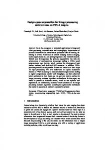
L. Briozzo SGS-Thomson Microelectronics Agrate Brianza, Italy I-20041 such materials is not straightforward. This problem has been already investigated using both standard image processing [1], [6] and neural [7], [2] approaches. data Line Scan Camera
data Acquisition & Pre-processing
Defect Detection ASIC Chip
control data
Host Computer
1 Introduction
Figure 1: Generic architecture of the defect de-
The Fluorescent Magnetic Particle Inspection method (FMPI) [4], is a technique used for the visual inspection for the quality control analysis in the production of mechanical parts: engines, etc. At rst, small magnetic particles of uorescent powder are distributed onto a uniform bar of ferromagnetic material that has been previously magnetized. If there are discontinuities at, or immediately below the surfaces, the density of the particles is higher next to them: the nal distribution of the powder on the surface evidences the presence of discontinuities mainly if the ferromagnetic material is illuminated by ultraviolet light. The automation of the visual inspection would improve inspection quality and increase productivity. Nevertheless, the automatic detection of defects in
The solution proposed in [2] seems to be suited for the digital VLSI implementation. In [2] an approach based on highly constrained neural networks with a few weights is proposed. The simulation results show that such approach is useful when the number of the test images is small and context informations have to be considered. We have modi ed the algorithm proposed in [2] and designed a digital architecture that exhibits real-time speed and e�cient detection. We have designed an ASIC chip that implements the digital architecture: it acts as a co-processor of a general purpose processor (Host Computer) that manages the I/O operations and an Acquisition and Pre-processing system (see Fig. 1). The chip receives in input an image of mechanical pieces treated using the FMPI technique and gives as output a binary code showing whether a physical defect is present or not in the piece. During the rst phases of the design, we evaluated
1 This work has been developed within a grant of the "Programma Nazionale di Ricerca per la Bioelettronica" assigned by the Italian Ministry of Scienti c and Technological Research to SGS-Thomson Microelectronics
tection system.
the precision constraints of the neural network architecture applied to our speci c application: we found that good detection results can be obtained with a reduced precision of computations. To this purpose, custom commercial chips are available, [3], [9], [5]; nevertheless, no one of them ts our computational needs. Consequently, the design of an ASIC chip looks to be the more attractive way for an e�cient hardware implementation of the neural architecture. Our paper is organized as follows: in Section 2 the neural network architecture is presented. The design methodology is illustrated in Section 3. Section 4 illustrates the chip architecture; the physical design of the chip is presented in Section 5. The conclusions are drawn in Section 6.
2 The Neural Network Architecture θ
Output Layer MAX MAX MAX MAX MAX MAX
Hidden Layer
Input
Figure 2: Structure of the network: for each
row of the hidden layer, the maximum value of neurons is computed and passed on to the output layer. � is a threshold used during the decision phase. Crack indications can be distinguished from edge indications or luminous re exes by studying the pro les of the bright lines in FMPI images. We devised a neural network that convolves the input image with an optimal lter (the lter pro le is determined by the weights of the network, o�-line learned with a Back-Propagation, [8], approach); then, through adequate, local, non linear post-processing the network obtains, from the convolution results, a binary output indicating the presence or not of one or more structural defects. The network detects defects that are mainly vertical in shape: to detect horizontal defects we can give in input to the network also the transposed image. The post-processing phase operates on small sub-matrices (28 � 24 pixels) of the convolved
image (508 � 504 pixels). The sub-matrices are partially overlapped. The operations performed by the neural network can be summarized as follows (see Fig. 2, which refers to a single input sub-matrix):
� Computation of the 2-D convolution of the input image. The input image has size 512 � 512 pixels (input layer) and the convolution mask has size 5 � 9 weights. Adjacent neurons are con-
nected, with the same weight distribution, to partially overlapped areas of the input image relative to masks shifted of 1 pixel. The neurons of the hidden layer (convolved image) are linear. � Partitioning of the convolved image into partially overlapped sub-matrices of size 24 � 28 pixels and computation of the maximum values of the neurons of each row of the sub-matrix (hidden layer). The operation of the maximum selection on the rows of the hidden layer makes the network insensitive to small changes of the orientation of the defect around the vertical direction. � Computation of the sum of the maxima and decision (comparison with a threshold) for the recognition of the defects for each sub-matrix (output layer). The neuron of the output layer has a sigmoidal transfer function. Its output, therefore, is a non linear transformation of the sum of all the selected maximum values. This operation makes the detection dependent on the uniformity of the defect pro le along the vertical direction.
3 Design methodology The design methodology (see [10]) is shown in Fig. 3. We started from a set of speci cations (system requirements), issued by the end user (e.g. size of the input image, size and features of the convolution mask, real time speed, heuristics for the decision about the presence of the defect etc.) and from the neural network architecture (e.g. topology of the network, functionality of neurons and synapses, learning algorithm, etc.) that was modeled and simulated at algorithmic level. We performed the VHDL high level modeling of the architecture and we identi ed the computational bottleneck (computation of the 2-D convolution); then we applied a set of high level transformations to the kernel of the 2-D convolution to meet the speci cations. The high level transformations identi ed quite easily
the micro-architecture of the data-path for the computation of the 2-D convolution (see [10]). The chip architecture was then described at RT-level; at the same time we devised the time scheduling and the resource allocation. No retiming iterations were needed. We modeled in a synthetizable way all logic blocks and, using a logic synthesis tool (Synopsys), we mapped the architecture onto a real circuit in the target technology. The output of the synthesis is an EDIF netlist that has been used as input for the physical design. The macro-blocks (e.g. RAMs) were generated using macro-blocks generators. System Requirements
High Level Modeling (VHDL)
WRITE LOOKUP TABLE
54 Bit
10 Bit
8 Bit
CONVOLUTION LINE 1
11 Bit
CONVOLUTION LINE 2
CONVOLUTION LINE 3
11 Bit
High Level Transformations (VHDL)
IN-OUT DATA BUS
CONTROL BUS
32 Bit
9 Bit
CONVOLUTION LINE 4
CONTROL UNIT OUTPUT PORT
Partitioning into Blocks
12 Bit 8 Bit
8 Bit
DECISION DATA BUS
Chip Architecture
MAXIMUM SELECTION
9 Bit
DECISION
12 Bit
CONVOLUTION LINE 5
14 Bit
Figure 4: Chip architecture.
Verification (VHDL simulation)
Verification (VHDL simulation) Verification (HDL simulation)
Chip Modeling for Synthesis Synthesis
6 Bit
INPUT PORT
Physical Design
PG Tape
Figure 3: Design methodology.
The design ow is mainly organized in two steps: i) a VHDL-based front end (speci cation, simulation and synthesis) phase; ii) back end (physical design) phase. The VHDL RT-level model of the chip has been extensively simulated to evaluate the correctness of the architecture. The clock and main timing signals tree generation was performed manually on the basis of the informations obtained by a delay evaluation tool. The physical design was performed using STUnicad, the design kit of SGS-Thomson based on Cadence Design Framework II. The delay evaluator is EARLY. The validation of the design at physical level was performed through HDL simulations (Verilog, see [11]) because of the e�ciency of Verilog and of the reliable cell library component models.
4 The Chip Architecture By applying the design methodology described above, we designed the ASIC architecture that is in-
troduced in this paragraph. The architecture is detailed in Fig. 4. The architecture is data ow dominated: the data path (blocks CONVOLUTION LINE i, 1 � i � 5, MAXIMUM SELECTION, DECISION, WRITE LOOKUP TABLE, INPUT and OUTPUT PORTs) occupies about the ninety per cent of the area of the chip and the CONTROL UNIT occupies the remainder. The ve CONVOLUTION LINE blocks compute the 2-D convolution of the input image. The MAXIMUM SELECTION block computes: i) the maximum values of the neurons of the rows of the convolved submatrices and ii) the sum of maxima. The DECISION block computes the decision about the presence of the defect. The INPUT/OUTPUT PORTs manage the multiplexing of Input (input image pixels) and Output (convolved image pixels) data on the IN-OUT DATA BUS. The WRITE LOOKUP TABLE block manages the loading of the weights during the initialization phase. The CONTROL UNIT controls the activity of the chip. The architecture of the CONVOLUTION LINEs is detailed in Fig. 5: each of them is made by a tree of adders (+) and multipliers (*). The synchronization of the data ow between the CONVOLUTION LINEs and the storage of partial results have been implemented using delay lines (bu�). Input and output pixels are 8 bit data; they are timemultiplexed, 4 data at a time, on the 32-bit IN-OUT DATA BUS. The chip gives as output a 1-bit data indicating the presence of the defect and an 8-bit data coding the 8 most signi cant bits of the sum of the maxima (DECISON DATA BUS). The chip features a deep pipeline organized in twolevels: the rst level inside single blocks and the second level between blocks. The pipeline management is based on a single-phase clocking scheme based on two di�erent clock signals: i) a high speed clock distributed on a small area (CONTROL UNIT); ii) a clock with a frequency half of the master clock frequency distributed all over the chip. Following this approach, the constraints on the clock skew are less severe and the clock signals can be handled more easily during the physical design phase. At rst, applying the cited design methodology, we optimized the computation of the 2-D convolution that turned to be the bottleneck of the overall architecture. Then we performed an accurate analysis on the precision of the computation needed by the neural architecture with the application at hand. Based on the previous results, we found that the multiplications involved in the computation of the 2-D convolution
can be e�ciently performed with a reduced precision. Consequently, the multipliers have been implemented using look-up-tables. Both the look-up-tables and the delays lines were implemented using RAMs. pixel_in delay line
0)
acc
acc
1) +
8) +
buff
Conv.1 buff
acc
acc
0) +
8) +
acc
acc
0) +
8) +
Conv. 2
buff
Conv. 3 buff
acc
acc
0) +
8) +
acc
acc
0) +
8) +
Conv. 4
pixel_out Conv.5
Figure 5: Architectural schema of the CONVO-
LUTION LINEs.
5 Chip Design The chip has been implemented in a 0:7�m CMOS technology (SGS-Thomson HCMOS4T, double metal, single poly): the chip complexity is of about 13,000 standard cells and 7 RAM macroblocks and the chip area is 10 mm � 0:9 mm. All physical checks (DRC, ERC, etc.) have been performed. At present time, the design is completed and it has been validated by the nal HDL simulations. The speed resulting from the HDL simulation, that takes into account the cell and wiring delays, is of 30 MHz for the master clock
(corresponding to 1.35 GOPS @ 30 MHz). The power consumption is of about 2 W. At such speed, the chip performance is beyond the speci cations. The following table summarizes the main features of the chip. Technology SGS-Thomson HCMOS4T CMOS 0.7 �m double metal, single poly Complexity 90000 equivalent gates Power cons. 2 W @30 MHZ Chip area 10mm � 0:9mm Speed 1.5 GOPS @ 30 MHz Package 100 PIN PGA
6 Summary and Conclusions In this paper, we presented the design of an ASIC chip for real-time image processing in industrial applications. The chip implements a neural network model tuned for the speci c application: defect detection in images of mechanical parts treated with the Fluorescent Magnetic Particle Inspection technique. We adopted an ad-hoc design methodology that allowed to attain real-time speed and a compact and (to a certain extent) modular design. At present time the design is terminated and it has been fully validated. The chip will be manufactured in a CMOS 0:7 �m, single poly, double metal technology within the end of this year. In the framework of this project, an industrial partner is being developing a demo/validation system for the chip.
Acknowledgements The authors would like to thank Dr. Luigi Ra�o, Dr. Paolo Faraboschi and Dr. A. De Gloria (DIBE, University of Genoa) and Dr. G. Voglino (SGSThomson Microelectronics).
References [1] Y.F. Chen, "Automatic Crack Detection with Computer Vision and Pattern Recognition of Magnetic Particles Indications", Material Evaluation, 42:1506, 1994. [2] N. Guglielmi, R. Guerrieri, M. Mastretta, and L. DeVena,"Highly Constrained Neural Networks with Application to Visual Inspection of Machined Parts", Proc. ICASSP93, pp. I 629-633, 1993.
[3] Inmos A110 DATABook. [4] D.C. Jiles, "Review of Magnetic Methods for non Denstructive Evaluation - part 2", NDT International, 23 (2), pp. 83 -92, 1990. [5] Plessey Semiconductors, PDSP 16488 DATABOOK.
[6] L. Ra�o, A. Blumenkrans, and D.D. Caviglia, "Defect Detection in Non Denstructive Testing Images by Hough Transform", Proc. Automation 1992 (Annual ANIPLA Congress), Genova (Italy), 1992. [7] L. Ra�o, D.D. Caviglia, and L. DeVena, "Neural Defect Detection in Magnetic Particle Inspection Test's Images", Proc. Image Processing: Theory and Applications, Sanremo (Italy), 1993. [8] D.E. Rumelhart, and J.L. McClelland, Parallel Distribuited Processing, MIT Press, Cambridge, Mass., 1986. [9] SGS-Thomson, Image Processing DATABOOK, 2nd edition. [10] M. Valle, M. Cornero, G. Nateri, D.D. Caviglia and L. Briozzo, "A VHDL-based Design Methodology: the Design Experience of an High Performance ASIC Chip", EURO-DAC'94/EUROVHDL'94 Conference, 1994. [11] M. Valle, "Design Validation of an ASIC Chip based on the Structural VERILOG Modeling and Simulation", Dibe Techn. Report, Nov. 1994.