ASIC Design Flow. By. P.Radhakrishnan,. Senior ASIC-Core Development
Engineer,. Toshiba,. 1060, Rincon Circle,. San Jose, CA 95132 (USA). Jan 2000
...
ASIC Design Flow
By P.Radhakrishnan, Senior ASIC-Core Development Engineer, Toshiba, 1060, Rincon Circle, San Jose, CA 95132 (USA)
Jan 2000 (Issue-3)
ASIC Design Flow
Contents Introduction...................................................................................................................... 3 Application Specific Integrated Circuits (ASIC)....................................................... 3 Frontend Design.............................................................................................................. 4 Coding ........................................................................................................................................................................... 4 Verification................................................................................................................................................................... 5 Synthesis ....................................................................................................................................................................... 5 Backend Design............................................................................................................... 6 Design Tools ..................................................................................................................... 6 Conclusion & Disclaimer............................................................................................... 7 Trademarks ................................................................................................................................................................... 7
2
Copyright © 2000 by P.Radhakrishnan. All rights reserved
ASIC Design Flow
Introduction This paper addresses some of the current trends that have been followed in the ASIC design. The amount of information that can be provided about this topic is so vast that one can write a complete book about the ASIC Design. However this paper addresses the important two phases of an ASIC design so that students can get an idea of how a chip is developed from concept to silicon. Due to the high demand for speed and performance, most of the functions that were implemented in the software are shifting towards the hardware. This means functions like the communication protocols, DSP algorithms, audio and video compression algorithms and many other functions find it most advantageous to be implemented in the hardware for meeting the performance. Another factor that leads to this situation is miniaturization. Due to the fast changes happening in the semiconductor technology the ability to pack more circuits in a small area has increased many fold. While the semiconductor companies are concentrating on the advanced technologies, the designers are increasing the complexity of the design by adding more and more logic in a single chip leading to the System-on-a-Chip (SoC) concept. This paper throws light on some of the key steps involved in realizing an ASIC.
Application Specific Integrated Circuits (ASIC) What is an ASIC? It is one other chip built to do a specific function. As mentioned above there are high demands in the industry to implement algorithms in hardware. As a result of this, many design groups implement specific functions in silicon in the form of an ASIC. In the olden days (about 10 years ago) the set of tools available for IC design were very limited, and there were a large amount of manual interventions. These days’ ICs are very huge and it is impossible to do them without the help of the EDA (Electronic Design Automation) tools. The EDA tools play a major role in the ASIC design flow and there are hundreds of companies functioning as EDA vendors supplying tools that help in various phases of the chip design. In the initial days when the EDA tools were evolving, tools were supporting the schematic entry. Schematics are the pictorial representation of the gates and flops of the design. You would draw the circuit in the same way as you would do in a paper. The schematic editor will have many capabilities to describe hierarchical design and also have capabilities to duplicate, cut, paste, etc. With these features one could build a circuit and edit them with ease. The tools took these schematics as inputs and generated database having connectivity information in them. The next version of tools accepted text entries in the form of Boolean equations and worked on the equation to get the desired logic. Since one can express any logic function in the form of a sum-of-product (SOP) or product-of-sum (POS) terms, these tools took the Boolean equations and run the optimizing algorithms to get the optimal logic which would meet the function and the timing. These optimizations are similar to the optimizations one wold do using methods like K-map. The current days’ designers use what are known as HDL (Hardware Description Language) for the design. HDL is a way of describing the logic and state machines
Copyright © 2000 by P.Radhakrishnan. All rights reserved
3
ASIC Design Flow
through equations and behavioural descriptions. The tools understand these descriptions and infer the necessary logic to implement the logic function.
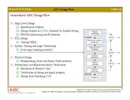
Frontend Design Fronend design is the first phase in the ASIC design where the logic for the chip is built using the HDL. The designer would write codes that would represent the function that he/she wants to implement. This logic realization is done using various steps in which the design is coded, verified and mapped to the actual gates using a process called synthesis. The rest of this section addresses to each one of these steps. Coding In the industry there are several HDLs being used. However there are two common hardware description languages that are very popular. They are, Verilog and VHDL. Though VHDL is a much older candidate, Verilog became very popular due to its “C” like syntax and constructs. There are plenty of arguments about which one is easier or better. In the recent years support for Verilog has been the prime focus of most of the EDA vendors. But there is always support for the VHDL codes also. No matter which language one uses for coding, the intention here is to express the design in the form of a behavioural description of code. For those who are wondering how these codes would look like, there is a very simple example given below. Complex functionalities will have numerous lines of codes distributed in many files. Example:1 (Verilog Code) // This line is a comment module test (clk, a, b, c, c_reg); input clk, a, b; output c,c_reg; reg c_reg; assign
wire c;
c = a || b;
// Logical OR of the signals a and b
// output of the previous step is sent through a flop that // is clocked by “clk” always @ (posedge clk) c_reg


![[Full] Physical Design Essentials: An ASIC Design ... - Google Sites](https://m.moam.info/img/260x300/full-physical-design-essentials-an-asic-design-goo_64783b01097c4744708c98f4.jpg)


