May 10, 1999 ... ASIC design team (Project leader, designers for different tasks). • Information
share ... is important! • Design flow must be defined and approved ...
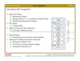
ASIC DESIGN FLOW
TKK “Laitteistokuvauskielinen digitaalisuunnitelu” Syksy-1999 MPl 5.10.1999
ASICS • What are ASICS? Any IC other than a general purpose IC which contain the functionality of thousands of gates is usually called an ASIC(Application Specific Integrated Circuit). ASICs are designed to fit a certain application.
•
An ASIC is a digital or mixed-signal circuit designed to meet specifications set by a specific project.
TKK “Laitteistokuvauskielinen digitaalisuunnitelu” Syksy-1999 MPl 5.10.1999
ASIC Project • ASIC design team (Project leader, designers for different tasks) • Information share with closely related projects/design teams (software, analog HW design, system design) - Documentation! • ASIC project is a part of bigger project - Scheduling is important! • Design flow must be defined and approved
TKK “Laitteistokuvauskielinen digitaalisuunnitelu” Syksy-1999 MPl 5.10.1999
ASIC Design Flow SYSTEM REQUIREMENTS
SPECIFICATION SPECIFICATION
LOGIC DESIGN MODELLING
LOGIC DESIGN
SYNTHESIS
VERIFICATION
TEST GENERATION
PHYSICAL
SIGN-OFF / Mapping
MANUFAC / Place & Route
/ Configuration data
PROTOTYPE SYSTEM TESTING PROTO VERIFICATION
SYSTEM TESTING
TKK “Laitteistokuvauskielinen digitaalisuunnitelu” Syksy-1999 MPl 5.10.1999
ASIC Specification • The goal is to specify the functional requirements for the design and define the external interfaces to the related designs. SYSTEM REQUIREMENTS
SPECIFICATION System Req. Specification System Func. Specification ASIC Project Plan Tools
e . g. Wo r d
Re qu i r e me n tS p e c i f i c a t i
REQ. SPEC REVI EW Re qu i r e me n t Spe c i f i c at i
e . g. Wor d
Da t a Sp e c ti f i c a t Sh i
DATA SHEET REVI EW
TKK “Laitteistokuvauskielinen digitaalisuunnitelu” Syksy-1999 MPl 5.10.1999
MODELLING
Da t a S he e t l 1
ASIC Modeling • The goal is to build a simulatable (behavioral) VHDL model corresponding to the specification. • The function of the model is verified by using a VHDL test bench • Architecture design • Model validation ok -> Logic design
TKK “Laitteistokuvauskielinen digitaalisuunnitelu” Syksy-1999 MPl 5.10.1999
Logic design • The goal is to write a synthezisable VHDL description of the design • Design rules (Naming, vendor independence, Use only IEEE standard types, comments, …). • Reusing • Synchronous design !! • Design partitioning (into RTL blocks)
TKK “Laitteistokuvauskielinen digitaalisuunnitelu” Syksy-1999 MPl 5.10.1999
Naming rules • Use meaningful names for signals, ports, functions and parameters. For example, do not use ra for a RAM address bus. Instead, use ram_addr or RamAddr (capital letters can also be used). • If your design uses several parameters, use short but descriptive names. • Use the name clk for the clock signal. If there is more than one clock in the design, use clk as the prefix for all clock signals (for example clk4m, clk8m). • Use the same name throughout the hierarchy for all clock signals that are driven from the same source. • For active low signals, end the signal name with an underscore followed by a lowercase character x. • Use the name reset for reset signals. For active low resets use the name reset_x. • For multibit buses, use (y downto x) ordering of bits. TKK “Laitteistokuvauskielinen digitaalisuunnitelu” Syksy-1999 MPl 5.10.1999
Naming rules • Use the same name or similar names for ports and signals, throughout the hierarchy, that are connected. (for example, a => a; or a => a_int;) • Use the name enab for an enable signal. If there is more than one enable in the design, use enab as the prefix for all enable signals. • Testbench is named 'name_of_the_block'_TB.
TKK “Laitteistokuvauskielinen digitaalisuunnitelu” Syksy-1999 MPl 5.10.1999
Guidelines for clocks and resets
The preferred clocking structure is a single global clock and positive edge-triggered flip-flops as the only sequential devices.
FF
clk
TKK “Laitteistokuvauskielinen digitaalisuunnitelu” Syksy-1999 MPl 5.10.1999
FF
Guidelines for clocks and resets • Digital ASICs must be designed to be synchronous when possible. This must be considered, when VHDL for synthesis is written. The main benefits of synchronous design are: • Timing problems are avoided. Only the propagation of signals to the next register during one clock cycle must be verified. • Most of the problems with hazards are avoided. • The X-states and glitches in gated and multiplexed clocks are avoided. • It is easier to test a synchronous circuit than an asynchronous one. • Static timing analysis is possible.
TKK “Laitteistokuvauskielinen digitaalisuunnitelu” Syksy-1999 MPl 5.10.1999
Guidelines for clocks and resets • partition the design so that all the logic in a single module uses a single clock and a single reset. • Isolating clock and reset generation logic in a separate module allows the other modules to use the standard timing analysis and scan insertion techniques. It also makes it easier to develop specific test strategies for the clock/reset generation logic. clk1 master clock
Clock Generation
clk2
clk3
TKK “Laitteistokuvauskielinen digitaalisuunnitelu” Syksy-1999 MPl 5.10.1999
submodule 1 submodule 2 submodule 3
Guidelines for clocks and resets • Avoid gated clocks • Clock gating circuits tend to be technology specific and timing dependent. Improper timing of a gated clock can generate a false clock or glitch, causing a flip-flop to clock in the wrong data. Also, the skew of different local clocks can cause hold time violations. • Gated clocks also cause limited testability because the logic clocked by a gated clock cannot be made part of a scan chain.
FF
clk
TKK “Laitteistokuvauskielinen digitaalisuunnitelu” Syksy-1999 MPl 5.10.1999
FF
Guidelines for clocks and resets • If your design requires gated clocks, use preferably vendor provided gated flip-flop elements using master clock.
data enable master clock reset
TKK “Laitteistokuvauskielinen digitaalisuunnitelu” Syksy-1999 MPl 5.10.1999
Guidelines for clocks and resets • Avoid internally generated resets • Make sure your registers are controlled only by a single reset signal. • Avoid internally generated, conditional resets if possible. Generally, all the registers in the macro should be reset at the same time. This approach makes analysis and design much simpler and easier. • If conditional reset is required, create a separate signal for the reset signal, and isolate this in a separate module. This approach results in more readable code and improves synthesis results.
TKK “Laitteistokuvauskielinen digitaalisuunnitelu” Syksy-1999 MPl 5.10.1999
Design partitioning • Good partitioning in the design provides several advantages including:
Easy handling of design requires sensible hierarchy Better synthesis results Faster synthesis compile runtimes Ability to use simpler synthesis strategies to meet timing Reusability
TKK “Laitteistokuvauskielinen digitaalisuunnitelu” Syksy-1999 MPl 5.10.1999
Design partitioning • Locate related combinational logic in a single module and single process if possible • The synthesis tool has more flexibility in optimising a design when related combinational logic is located in the same module. This is because synthesis tools cannot move logic across hierarchical boundaries during compile operation. A
B
clk
FF A
COMB A
C
COMB B
A
clk
FF C
Bad
C
clk
FF A
COMB A&B&C
clk
A
FF C
Better
C
clk
FF A
COMB A&B&C
TKK “Laitteistokuvauskielinen digitaalisuunnitelu” Syksy-1999 MPl 5.10.1999
COMB C
clk
FF C
Best
RTL block design P RTL titi Bl k
VHDL Sch.,DFD
RTL Bl o c k D i
Ar c hi t e c t u r e Pl i d l A a n/ hi De s c r i p t M
Te x t di
Sy nt he s i z a b l e Bl oc k RTL D i
RTL VHDL
Target technology
Tar ge t h dal t a b
VHDL
De s i g n C il
Syn t h e s i s Ch k
Schematics
S c h e mat i c i
VHDL TB
VHDL Te s t Be n c h Me n t o r VSS Si l
RTL Bl o c k F ti V ifi ti
RTL Doc Bl ume k nt a t i o
simulation results
S t i mu l iRe s po ns e VHDL,DFD
Add e d c o mme n t s Te x t di Bl o c k Re v i e w
RTL Block
Re l e a s e d RTL bl k
RTL Mod e l I nt e g r a t i
TKK “Laitteistokuvauskielinen digitaalisuunnitelu” Syksy-1999 MPl 5.10.1999
Synthesis LOGIC DESIGN
SYNTHESIS
VHDL
RTL VHDL Mode l
e . g. Te x t di Generic technology
Ge n e r i c h dat l a b
S e pa Pr t h r a ti i
VHDL Sch.,DFD
RTL VHDL Mode l opt i mi z e d f or h i Mo dul e Syn t he s i
Schematics
Sc h e mat i c bas e d on ge i ne r i c h l
De s i gn Compi l e r Te s t Comp i l e r M Lia pb pi ng
Schematics
Sc h e mat i c bas e d on ti ar ge t h l Target technology
ASI C t e s t s yn t he s i s , t t bi l i t
Tar ge t h dat l a b
Schematics
Sc h e mat i c add e d t e s ti s t r u c t ur e
M d i mi Opt l zat i
Schematics
Sc h e mat i c opt i mi z e d i f or t ar ge t h l Ti mi ng A l i Ti mi ng R
VERIFICATION
TKK “Laitteistokuvauskielinen digitaalisuunnitelu” Syksy-1999 MPl 5.10.1999
Gate level verification
CHIP VERIFICATION ASI C/ FPGA RTL d i i
Opt i mi z e d db
Synthesis
Static timing analysis Sy nops y s De s i gn or FPGA r e nt orc ompi e quil ve al l
Qui c k c he c k Ti mi ng
Netlist creator
Ne t l i s
Formal verification
Sy nt he s i s Li br ar
and ASI C/ FPGA gat e Li b Te s t be nc h, be h. mode l
St i mul i Re ds pons e s
static timing analyses
Functional simulation
Aut omat i c / manua lc ons t r ai n Functional errors
Mapping (FPGA)
VHDL/ gat e l e v e l i l
Floorplanning
ASI C/ FPGA v e ndor td ooli s
Place&route (FPGA)
ASI C/ FPGA Ce l l Li b
Mappi ng i nf or mat i
Fl oor pl anni n i nf or mat i
FPGA i mpl e me nt at i
Static timing analysis Ti mi ng
Te s t be nc h, be h. mode l
St i mul i Re ds pons e s
Timing simulation Dat a She e t d
VHDL/ gat e l e v e l l t i
TKK “Laitteistokuvauskielinen digitaalisuunnitelu” Syksy-1999 MPl 5.10.1999
Timing errors
TO TEST GENERATION
Test generation CHIP VERIFICATION
Chip gate level schematic with test structures TEST GENERATION
(ASIC only)
Pr e l i m. t e s t pa t t e r n ti
Ma nu a l t e s t pa t t e r n ti
Test Patterns
ASCI I Pr e l i mi na r y
Test Pattern
ASCI I Man ua l : RAM . .
Test Compiler Plus
Au t o ma t i c p t at t er n i
Te s t Si t i mull a t i o n
Test Pattern
ASCI I Aut omat i c Test pattern responses
ASCI I Te s t da t a : s t i mu l i +
VeriFault
Fa u l t G di Ve r i f i e d Ch i p h i
Layout
TKK “Laitteistokuvauskielinen digitaalisuunnitelu” Syksy-1999 MPl 5.10.1999
Layout and sign off TEST GENERATI ON
Schema Netlist
Lay o ut
De s i gn , t e s t d a t a
(ASIC)
Ve n d or s De s i gn Ki
Pr e l a yo ut i l ti
simulation results
S t i mul iRe s p on s e
Pl a c e & Rou t e Design
Target technology
GDS I I
Tar ge t h dat l a b Po s t l a y ou t i l ti
Ba c k a nn ot a t e t o S St a t i c Ti mi ng A l i
De s i gn DRC, i f i LVS ti Ve n d or l fil
simulation results
S t i mul iRe s p on s e
Back annotation
Ti mi ng f i l e t o d i
Re p o r t fil
Si g n o f f Man u f a c t . a g r e e me nt
MANUFACTURI NG PROTO TESTI NG
TKK “Laitteistokuvauskielinen digitaalisuunnitelu” Syksy-1999 MPl 5.10.1999
Prototype testing • Final verification is done with E/S (engineering samples). • Physical measurements: Parametric DC tests Parametric AC tests Functional tests Power consumption Thermal tests
• Release to system tests • Final documentation and project completion • Chips manufacturing
TKK “Laitteistokuvauskielinen digitaalisuunnitelu” Syksy-1999 MPl 5.10.1999
FPGA prototyping • FPGA, Field Programmable Gate Array • VHDL coding for FPGAs (design partitioning, limited maximum clock speed, limited amount of interfaces) • Building prototyping board • Prototyping in laboratory environment
TKK “Laitteistokuvauskielinen digitaalisuunnitelu” Syksy-1999 MPl 5.10.1999
FPGA prototyping • Advantages: VHDL is tested with real clock speed, in real environment Prototyping environment offers "early ASIC" for other projects More secure to sign off
• Disadvantages Requires a lot of time and resources Expensive
TKK “Laitteistokuvauskielinen digitaalisuunnitelu” Syksy-1999 MPl 5.10.1999


![[Full] Physical Design Essentials: An ASIC Design ... - Google Sites](https://m.moam.info/img/260x300/full-physical-design-essentials-an-asic-design-goo_64783b01097c4744708c98f4.jpg)


