ATSI- Research Unit, ISSATSO, University of Sousse, Tunisia. Abstract. For real-
time applications, there are several factors (time, cost, power) that are moving ...
T RANSACTIONS ON D ATA P RIVACY 3 (2010) 43 —64
Design and Hardware Implementation of QoSS‐AES Processor for Multime‐ dia applications Zeghid Medien**, Mohsen Machhout*, Belgacem Bouallegue*, Lazhar Khriji***, Adel Baganne**, Rached Tourki* * Electronic and Micro‐Electronic Laboratory, Faculty of Sciences of Monastir, 5000, Tunisia. E‐mail:
[email protected] ** Laboratoire des Sciences et Techniques de lʹInformation, de la Communica‐ tion et de la Connaissance (Lab‐STICC), CNRS: FRE2734 –University of South Brittany, Lorient, France. E‐mail: adel.baganne@univ‐ubs.fr *** ATSI‐ Research Unit, ISSATSO, University of Sousse, Tunisia. Abstract. For real‐time applications, there are several factors (time, cost, power) that are moving security considerations from a function centric perspective into a system architecture (hardware/software) design issue. Advanced Encryption Standard (AES) is used nowadays extensively in many network and multimedia applications to address security issues. The AES algorithm specifies three key sizes: 128, 192 and 256 bits offer‐ ing different levels of security. To deal with the amount of application and intensive computation given by security mechanisms, we define and develop a QoSS (Quality of Security Service) model for reconfigurable AES processor. QoSS has been designed and implemented to achieve a flexible trade‐off between overheads caused by security ser‐ vices and system performance. The proposed architecture can provide up to 12 AES block cipher schemes within a reasonable hardware cost. We envisage a security vector in a fully functional QoSS request to include levels of service for the range of security service and mechanisms. Our unified hardware can run both the original AES algorithm and the extended AES algorithm (QoSS‐AES). A novel on‐the‐fly AES encryp‐ tion/decryption design is also proposed for 128‐, 192‐, and 256‐bit keys. The performance of the proposed processor has been analyzed in an MPEG4 video compression standard. The results revealed that the QoSS‐AES processor is well suited to provide high security communication with low latencies. In our implementation based on Xilinx Virtex FPGAs, speed/area/power results from these processors are ana‐ lyzed and shown to compare favorably with other well known FPGA based implemen‐ tations.
43
44
Zeghid, Machhout, Bouallegue, Khriji, Baganne, Tourki
1
Introduction
Security issues involved in embedded systems ranging from low‐end systems such as networked sensors, wireless handsets, PDAs, and smart cards to high‐ end systems such as routers, gateways, firewalls, storage servers, and web serv‐ er become more and more important. For such systems, there are several factors governing security from a function centric perspective to a system architecture (hardware/software) design issue. For example: The processing capabilities of many embedded systems are easily overwhelmed by the computational de‐ mands of security processing, leading to undesirable tradeoffs between security and cost, or security and performance. Battery‐driven systems and small form‐ factor devices such as PDAs, cell phones and networked sensors often operate under stringent resource constraints (limited battery, storage and computation capacities). These constraints go worse when the device is subject to the demand of security like real‐time multimedia applications that will impose requirements for time. Embedded system architectures need to be flexible enough to support the rapid growth of security mechanisms and standards. Cryptographic Algo‐ rithms that require increasing computation capabilities are developed such as AES. In November 2001, the National Institute of Standards and Technology (NIST) of the United States chose the Rijndael algorithm as the suitable AES [3] to re‐ place the Data Encryption Standard (DES) algorithm [1]. There are three kinds of choice for the cipher key of the AES: 128‐, 192‐ and 256‐bit, called AES‐128, AES‐192, and AES‐256, respectively [3]. AES has 10 rounds for 128‐bit keys, 12 rounds for 192‐bit keys, and 14 rounds for 256‐bit keys. The design and strength of all key lengths of the AES algorithm are sufficient to protect classified infor‐ mation up to the SECRET level. AES provides three levels of security: 128, 192, and 256 bits. AES, very low memory requirements, make it very well suited for restricted‐space environments, for which the AES exhibits high performance. The AES algorithm is used in some applications such as smart cards, cellular phones and image‐video encryption. The efficiency of hardware implementa‐ tions of the AES has been used by the designer as major criterion. Since then, many hardware implementations have been proposed in literature [12‐24]. Some of them use Field Programmable Gate Arrays (FPGA) and others use Application‐Specific Integrated Circuits (ASIC). Despite the advantage of a software implementation that includes ease of use, ease of upgrade, portability, and flexibility, it suffers from its limited physical security, especially with re‐ spect to key storage. Conversely, cryptographic algorithms (and their associated keys) implemented in hardware are, by nature, more physically secure, as they cannot easily be read or modified by an outside attacker. Reconfigurable hard‐ ware devices such as FPGAs are promising alternatives for the implementation T RANSACTIONS ON D ATA P RIVACY 3 (2010)
Design and Hardware Implementation of QoSS‐AES Processor
45
of block ciphers. FPGAs are hardware devices whose functions are not fixed and can be programmed in‐system. To deal with the amount of system performance and intensive computation given by security mechanisms, this paper provides a motivation for understand‐ ing QoSS and variant security for AES, and how these concepts may benefit variant applications and systems designs. So, we define and we develop a QoSS model for reconfigurable AES processor. The proposed architecture can provide up to 12 AES block cipher schemes within a reasonable hardware cost. Using a security vector, the user can assign a precise security service of his application (cryptographic operation, mode, key‐length, rounds number, quality of key, throughput). Our unified hardware architecture can run the original AES algo‐ rithm and the extended QoSS‐AES algorithm as well. Furthermore, this paper proposes a video encryption scheme, which includes the QoSS‐AES processor. Such a processor encrypts the DC DCT (discrete cosines transform) transform coefficients of each block in digital video. Since DC coefficients play an impor‐ tant role in MPEG video data, the method is designed to provide relatively high level of security for DC coefficients. The paper is structured as follows: The next section details the proposed archi‐ tecture and the overall design of the AES implementation. Also presented are the area and timing. Issues related to security levels of the cryptosystems con‐ sidered are discussed in section 3. The QoSS module is defined s well. Section 4 explains the details of our design on the QoSS‐AES cryptographic processor and compares the performance of our design to earlier ones. The illustration of the usefulness and the efficiency of the proposed processor through communication examples using an MPEG4 decoder are described in Section 5. Finally, conclud‐ ing remarks are made in Section 6.
2 2.1
Choice of an Architecture for AES Processor Our Choice
The choice of a suitable architecture has a significant impact on system per‐ formance. Different metrics can be used for this purpose; such as throughput, power consumption, area, security levels, resistance to side channel attacks, synchronous or asynchronous architecture and modes of operation. To this end, our objective is to define appropriate architecture for the AES processor. So far, the basic techniques for implementing a block cipher with rounds are iterated, pipelined, and loop‐unrolled architectures. The iterated architecture leads to the smallest implementation. Such architecture consists in a round component, which is fed to its output. The pipelined architecture contains all of the rounds as separated components. As a result, it is the fastest in terms of throughput and T RANSACTIONS ON D ATA P RIVACY 3 (2010)
46
Zeghid, Machhout, Bouallegue, Khriji, Baganne, Tourki
the largest of the basic structures. The loop‐unrolled architectures achieve two or more rounds per clock cycle and the execution of the cipher is iterated. In a pipelined architecture, unrolling can only decrease the latency of outputting the first block. In sub‐pipelining, registers are placed inside the round component in order to increase the maximum clock frequency. In the partial pipelining scheme, the pipeline contains the half of the rounds with registers in between. So, pipelined and loop‐unrolled architectures enable very high‐speed imple‐ mentations; but they imply large area and high power consumption. This fact makes them unattractive for embedded systems, such as smart cards. Further‐ more, they cannot be fully exploited in feedback modes of operation. Feedback modes are often used for security reasons in encryption and for Message Au‐ thentication Code (MAC) generation. In feedback modes, like Cipher Block Chaining (CBC) and Cipher Feedback (CFB) mode, it is not possible to start by encrypting the next block of data before the encryption of the previous block is completed. As a result, all blocks must be encrypted sequentially, with no capa‐ bility for parallel processing. In the non‐feedback modes, like Electronic Code Book (ECB) mode and counter (CTR) mode, encryption of each subsequent block of data can be performed independently from processing other blocks, thus all blocks can be encrypted in parallel. The basic iterative architecture assures the maximum speed/area/ratio for feedback operating modes (CBC, CFB). It is commonly used for bulk data en‐ cryption and, also, to guarantee near optimum speed, and near optimum area for these operating modes. The width of the AES data path can be further re‐ duced to decrease logic area and power. Hence, we chose the basic synchronous iterative architecture in our implementation. The subsection below presents the details of the design.
2.2
AES implementation using an iterative design
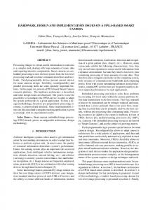
Figure 1 shows the block diagram of the different units of the AES‐128 based processor. As seen, the AES‐128 core includes the following units. The Input and Output interfaces take care of reading input data and writing encrypted output and are responsible for feeding the key logic. They are controlled by the data‐ready, ciphertext‐ready and clk signals. When the bus puts a data to be read or write this signal is selected and the data is taken. Library Functions: the different AES functions in this library, such as Sub‐ Bytes, inv‐SubBytes, ShiftRows, inv‐ShiftRows, MixColumns, inv‐ MixColumns and AddRoudkey are defined. Sbox ROM: is the direct implementation of the substitution boxes using loo‐ kup tables, because all of the 256 cases of the substitution bytes can be pre‐ computed and can be stored in a lookup table. T RANSACTIONS ON D ATA P RIVACY 3 (2010)
Design and Hardware Implementation of QoSS‐AES Processor
47
RAM keys: are used to load the initial key to the FPGA through the input interface. Key Expander is used to compute a set of round keys based on a ciphered key. Controller is used to generate control signals for all other units. Among other actions, the controller determines when to reset the cipher hardware, to accept input data and to register output results. Since the execution of MixColumn function is conditional (Figure 2), the controller decides wheth‐ er the result obtained by MixColumn is to be used or ignored. AES‐Round, used to encrypt or decrypt input blocks of data. In our application, ECB/CBC mode of operations is employed for data confi‐ dentiality and authentication. Ciphertext ready
Controller Data loaded Roundi
Done
Data ready Encrypt Data
Input Buffer
Data
AES-Round Key ready
Sbox Rom
Output Buffer
128 bits
128 bits
32 bits
Ciphertext
Ciphertext 32 bits
Roundkey
Start
Key Expander Key
128 bits
Ram Keys
Library Functions AES transformations SubBytes,inv-SubBytes MixColumns,inv-MixColumns ShiftRows, inv-ShiftRows
Figure 1. Iterative design of the AES‐128 processor
2.2.1
Proposed Architecture
The encryption‐decryption datapath of the iterative AES‐128 core is based on the single round implementation of the AES algorithm. The same datapath is used for the 10 rounds in the AES‐128 algorithm. Each round is performed in a single clock cycle except the first round (round zero) that only performs the key addition phase. The other 10 rounds perform the four different steps of the AES algorithm namely SubBytes, Shiftrows, MixColumns (not done last round), and AddRoundKey. Therefore, it takes total of 11 cycles to encrypt or decrypt a 128‐ bit block of data. As shown in figure 2, five logic blocks compose the overall AES Round. The component implementing the function AddRoundKey is simply a net of XOR gates that adds in GF(28) the round key to the current state. The component implementing the function SubBytes uses 16 S‐boxes stored in a Read‐Only Memory (ROM). The state obtained is row‐shifted. T RANSACTIONS ON D ATA P RIVACY 3 (2010)
48
Zeghid, Machhout, Bouallegue, Khriji, Baganne, Tourki
AES transformations SubBytes,inv-SubBytes MixColumns,inv-MixColumns ShiftRows, inv-ShiftRows
Muxselect
Data-round (128 bits) MixColumns\ Inv-MixColumns
Mux
Data Tmp
Done
Addroundkey
Round-data
Library Functions
ShiftRows \ Inv-shiftRows
The MixColumns function is implemented using a chain of XORs which results in the minimum delay implementation for this unit. The AES‐128 encryption and decryption data path is optimized to have a minimum delay for each round.
SubBytes \ Inv-SubBytes
RoundKey(i)
Mixselect
Figure 2. AES Round block implementation
Overall, the total combinational delay of all the four steps of the AES‐128 are minimized so that each round of the AES‐128 algorithm is performed in a single clock cycle at a maximum clock frequency. The decryption process follows the same order as the encryption, except for another round of mixed columns on the generated round key.
2.2.2
Experimental Results
We have implemented AES using the technique mentioned above. The AES‐128 encryption/decryption system is captured using VHDL. The Xilinx ISE tools have been used for the implementation of the design and the simulation envi‐ ronment is Modelsim. Xilinx XC2V1000 has been chosen as the target device. The architecture is simulated to verify the functionality, with use of the test vec‐ tors provided by the AES‐standard [3]. In order to have a fair and detailed eval‐ uation, we implemented AES‐128 encryption separately. Performance metrics such as area, throughput, and power consumption are used. Table 1 presents detailed results for these implementations. The process en‐ gine is able to operate in feedback mode at 159 MHz, which equates to 1.850 Gb/s. During self‐test at 50 Mhz, the process consumed 22.7mW. Table 2 compares our implementations with recent works reported in litera‐ ture in terms of AES‐128 encryption only, AES‐128 decryption only, both en‐ cryption and decryption [17], [24]. Comparisons with AES ASICs implementa‐ tions are also given [12], [13], [14]. As is shown, the throughput of our imple‐ mentation is better compared to that reported in [17]‐[18]‐[19]‐[20]‐[23]‐[24], but is lower than that in [21]. T RANSACTIONS ON D ATA P RIVACY 3 (2010)
Design and Hardware Implementation of QoSS‐AES Processor
49
Table 1. Results of the iterative AES‐128 design Performance metrics Design
Freq (Mhz)
AES‐128‐encryption XC2V1000 AES‐128‐encry/decryp XC2V1000
Area (slices)
Power (mW)
Throughput (Mbps)
159
1743
22,7
1850
82
3555
37,50
1049
Table 2. Performance Comparison Results Reference
Architecture
Area
Frequency (MHz)
Throughput (Mbps)
AES‐128: ASIC Implementation [12]
Non pipelined integrated
173k gates
154
2290
[13]
Non pipelined Decryption
58,43k gates
200
2008
[14]
[17] XCV300 [18] XC2V1000 [19] XCV1000E [20] XCV812 [21] XC2V1000 [22] Virtex‐II [23] Virtex‐II Pro [24] XC2V1000
Our works XC2V1000 Our works XC2V1000
Non pipelined 200,5K 66 Encry/Decry gates AES‐128: FPGA Implementation Non pipelined 2358 CLB 22 Encry/Decry Non pipelined 4325 75 Encry/Decry Non pipelined N/A 38,8 Encry/Decry Non pipelined 2744 20,192 Encryption Non pipelined 1122 159 Encryption pipelined 1937 182 Encryption Non pipelined 2703 LUT 196 + 44 BRAM Encryption Non pipelined 586 slices 96,42 + 10 BRAM Encryption Proposed architectures Non pipelined 1743 159 Encryption Non pipelined 3555 82 Encry/Decry
T RANSACTIONS ON D ATA P RIVACY 3 (2010)
844.8 (AES‐128) 704 (AES‐192)
259 739 451,5 258,5 1941 2118 1190 1450
1850 1049
50
Zeghid, Machhout, Bouallegue, Khriji, Baganne, Tourki
3
Quality of Security Service Requests
Quality of Service (QoS) mechanisms benefits both the user and the overall distributed system. QoS users profit by having reliable access to services. The distributed systems whose resources are QoS managed present the advantage to have more predictable resource utilization and more efficient resource allocation. Also, QoS involves user requests for levels of services which are related to performance‐sensitive variables in an underlying distributed system. To include the security as a real part of QoS, the security choices should be presented to users, and the QoS mechanism must be able to modulate related variables as well. References to security in the QoS literature are reported in [25]‐[26]. The term Quality of Security Service (QoSS) refers to the use of security as a quality of service dimension. To recap, the enabling technology for both QoSS and a security‐adaptable infrastructure is the variant security. It can be considered as the ability of security mechanisms and services to allow the amount (i.e. kind or degree) of security to vary within predefined ranges. In the following an analysis of the security in the designed AES processor will be presented.
3.1
Multilevel Security
The information is classified into different levels of trust and sensitivity. These levels represent the well‐known security classifications, namely, Low, Medium, and High security. They form a simple hierarchy where the data flows from Low level to High level, as illustrated in figure 3. High security
AES-256 AES-192
Medium
Security
AES-128
Low Security
Unclassified
Figure 3. The hierarchical security levels
The U.S National Security Agency (NSA) has conducted a review of the AES encryption algorithm and its applicability to protect national security information. In June 2003, the NSA review determined that the design and the strength of all three AES key lengths are sufficient to protect classified U.S government information up to the ʹSECRETʹ level. Their review concluded that T RANSACTIONS ON D ATA P RIVACY 3 (2010)
Design and Hardware Implementation of QoSS‐AES Processor
51
only the AES 256‐bit key length is strong enough to protect classified information at the “High security” level (top level security). Furthermore, the key length in AES could be used as a variable quality of security service. The QoSS function is given by, QoSS = f (key − length) (1)
3.2
Rounds Number Analysis
The presence or absence of shortcut attacks for a cipher is still considered as a quality criterion that is widely accepted in the cryptographic community. Fur‐ thermore, the resistance of iterative block ciphers with respect to a specific cryp‐ tanalytic method can be evaluated by performing attack on reduced‐round ver‐ sions of the block cipher. Such attacks can provide more information on the se‐ curity margin of a cipher. If, for R rounds cipher, there is a shortcut attack against a reduced‐round r (0