Design of low power 4-bit flash ADC based on standard cells Authors: Marcel Siadjine Njinowa*, Hung Tien Bui*, François-Raymond Boyer** * Department of Applied Sciences, Université du Québec à Chicoutimi ** Department of Computer Engineering, École Polytechnique de Montréal Members of ReSMiQ research group. Published in: New Circuits and Systems Conference (NEWCAS), 2013 IEEE 11th International Conference dates: 16-19 June 2013 DOI: 10.1109/NEWCAS.2013.6573626 Publisher: IEEE © 2013 IEEE. Personal use of this material is permitted. Permission from IEEE must be obtained for all other uses, in any current or future media, including reprinting/republishing this material for advertising or promotional purposes, creating new collective works, for resale or redistribution to servers or lists, or reuse of any copyrighted component of this work in other works.
Design of Low Power 4-Bit Flash ADC Based on Standard Cells Marcel Siadjine Njinowa,Hung Tien Bui
François-Raymond Boyer
Department of Applied Sciences Université du Québec à Chicoutimi
[email protected],
[email protected]
Department of Computer Engineering Ecole Polytechnique de Montréal
[email protected]
Abstract—In this paper, a standard cell low power 4-bit flash analog-to-digital converter (ADC) is proposed. The converter utilizes comparators created using only logic gates for converting analog input signals to digital values. This novel flash architecture consists of several CMOS gates with inputs connected to a common input node or to one of the supply lines. Depending on the relationship between the input signal and a given gate’s threshold voltage, the output will either be ‘0’ or ‘1’. The comparator is followed by an encoder to convert the thermometer code to binary code. Low power consumption is achieved by switching off the unused parallel voltage comparators. The proposed ADC was implemented at the transistor level in a 180nm CMOS technology with a 1.8 V supply voltage and was simulated using Cadence Spectre simulator. Simulation results show that for the same speed, this ADC provides about 70% power reduction compared to a previously proposed design.
I.
INTRODUCTION
The ADC is a key component in many modern electronics systems. For high-speed applications, flash and pipeline ADCs are often used. The flash type is the faster of the two, but limited to lower resolution and consumes more power due to a large number of components. In applications such as onchip direct digitization of a wideband RF signal and digital receivers, flash architectures are often preferred [1]. Many flash ADCs architectures [2-4] are reported in the literature. Traditionally, flash converters include 2N-1 comparators for N-bit resolution and have the advantage of having a very high sampling frequency. However, this structure occupies a large area and consumes a large amount of power when its resolution becomes high. This is not desirable for low power applications. To improve the design of flash type converters, several architectures have been proposed such as the two-stage architecture [5, 6], the folding and averaging converters [7, 8]. The major issue with these approaches is that it uses analog components that are difficult
978-1-4799-0620-8/13/$31.00 ©2013 IEEE
to integrate and whose performances are degraded as technology scales down. Furthermore, these ADCs need high gain differential comparators that are inherently more complex and require a resistor ladder circuit to deliver reference voltages. Other disadvantages of this approach are the reduction in throughput and poor differential linearity. Recently, some authors have proposed simple and faster flash converters based on the TIQ technique (Threshold Inverter Quantization) [9-12]. Although this technique reduces the complexity of the converter, it is sensitive to process variation and consumes considerable power. The idea behind this technique is to use the digital inverter as an analog voltage comparator. By keeping the transistor length constant and by varying its width, one can adjust the comparator’s threshold. Varying the transistor width to obtain correct configuration, however, is a long and repetitive task. To reduce the required design time and also reduce the risk of having non functional designs, it is therefore interesting to investigate ways to migrate these designs into a more digital form by using standard-cells. In this paper, we propose an ADC that can be fully implemented using only standard-cells. This allows the designer to stay within the mature digital design flow and effectively reduce risks and time-to-market. The rest of this paper is organized as follows. In Section II, the design of the ADC is described in details, considering each basic building block. Section III reports the transistor-level simulations of the proposed flash ADC. Finally, conclusions are drawn in Section IV.
II.
ADC DESIGN
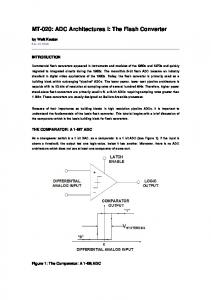
The proposed 4-bit flash architecture shown in Fig. 1 consists of two main components: a bank of comparators and an encoder.
whose inputs are respectively connected to VIN and ‘1’. In such a configuration, the gate operates like an inverter but the threshold will be lower than that of the inverter. In addition, by connecting a gate parallel to an initial gate, one can also increase or decrease its threshold voltage. Mathematically, the threshold voltage of a gate calculated as being [12]: VG TH =
C
C C
Figure 1.Proposed 4-bit flash ADC
A. Comparator Flash ADCs generate the output by comparing the input signal with all the reference voltages. In the case of the proposed system, the threshold voltage of each gate serves as a reference voltage. We define the threshold as the input voltage at which the output voltage is VDD/2. The comparators with a threshold voltage above the input value will output ‘0’ whereas the ones with lower threshold voltages will output ‘1’. This is what generates the thermometer code output. To explain the principle of operation, let us consider a Kinput NAND (K=2, 3, 4) gate whose inputs are connected together. In such a configuration, the gate operates much like an inverter. If the NMOS and the PMOS gates had identical VTH and were sized to have identical µCOX(W/L), the threshold of the NAND would be higher than that of the inverter and NOR gates. This is because, for the same VGS, the PMOS network would generate more current since it has a parallel connection whereas the NMOS network has a series connection. For the currents to be equal, the NMOS transistors would need to have higher VGS which explains the rise in gate’s threshold voltage. A similar reasoning can be applied to NOR gates. Let us consider a 2-input NAND gate
VDD − VTH + M ⋅ VTH M +1
(1)
In this equation M is the number of NMOS transistors connected in parallel (M becomes fractional when NMOS are connected in series), VTH is the threshold voltage of both PMOS and NMOS transistors and VDD is the supply voltage. Using this technique,
however, one of the drawbacks is the limited input voltage range which is limited to between VTH and VDD-VTH. In the proposed architecture, the logic gates include controllable inputs to allow the gates to operate in stand-by or active mode. For active mode, the controllable inputs of NOR gates are set to ‘0’ and those of the NAND gates are set to ‘1’.This situation is shown in Figure 1. It is important to note that the inverter at the top of this figure is set to ‘0’. The purpose of this is to increase the threshold of this comparator. For stand-by mode, the controllable inputs of NOR gates are set to ‘1’ and those of the NAND gates are set to ‘0’. In this case, the NAND and NOR gates output ‘1’ and ‘0’ respectively for any given input. This leads to a reduction in power consumption of the comparator in the case where the input voltage is not VDD or VSS and the ADC is not in operation. When the comparator consists of a NAND and a NOR gate, this type of connection can lead to a short circuit current. However, tests show that this short circuit current dissipates less power than the power it saves by going into standby. B. Encoder The encoder is often found to be the bottleneck of many flash ADCs. To help maximize operating speed, the proposed design uses the Fat-tree method [13, 14] since it is faster than other types of encoders. III.
SIMULATION RESULTS
In this section, the functional simulation of the proposed ADC is presented. In addition, a thorough characterization process was performed to ensure its suitability for high speed and low power applications. A. Functional Simulation To ensure the functionality of the design, transient and DC analyses were performed. The simulation results from Fig. 2 show that the output results are correct. The top plot shows the voltage ramp introduced at the input for the simulation. The four bottom plots show the output of the ADC, with the lowest plot representing the LSB. It can be shown from the figure that the bit duration at the output is not even. This is not due to a non-linearity issue but rather to uneven response
and step width is small. In absence of device mismatch, the error is bounded within ± 0.005 LSB.
0.2
IN L i
0.2
DNLi
times of the different comparators. Fig. 3 shows the DC response of the proposed ADC. This figure shows that the intervals between two adjacent comparators are similar thus minimizing the risk of having missing codes. As previously mentioned, the input voltage range is limited to between VTH and VDD-VTH. With the chosen fabrication technology, this translates to a minimum value of 0.587v and a maximum of 1.102v. For a 4-bit ADC, the LSB value is found to be 36.7mV.
0
-0.2
2 4 6 8 10 12 14
i a) DNL
0
-0.2
2 4 6 8 10 12 14
i b) INL
Figure 4. a) DNL and b) INL Curves for the Proposed 4-bit ADC
Figure 2. Transient Analysis of 4-Bit ADC
Figure 3. DC Response of the Proposed 4-Bit ADC
B. Spefications In order to ensure that the conversion errors of the proposed ADC are within the specification limits, it is important to perform tests to validate it. In this paper, these conversion errors are characterized by the differential non linearity (DNL) and integral non linearity (INL) as shown in fig. 4. From these figures, we can observe that any deviation from the ideal line
To measure the dynamic parameters of the ADC, an ideal sine wave is applied to the input and the digitized output signal is converted to its frequency-domain representation. The frequency domain representation is used to characterize the dynamic parameters of the ADC. In our test, the input signal is a 1MHz sine wave. The ADC outputs a digital sine wave which is converted back into the analog domain using an ideal DAC and a low-pass filter. Both the input and the resulting sine waves are shown in Fig. 5. The frequency domain representation of the output signal is shown in Fig. 6 where the fundamental component is at 1 MHZ. From this spectral representation, the ADC dynamic parameters can be measured. The signal-to-noise ratio (SNR) and spurious-free dynamic range (SFDR) values are respectively 56.14 dB and 25.16 dB which are considered adequate [4]. The performance comparison between the proposed ADC and state-of-the-art designs is presented in Table I. In terms of power consumption and conversion speed, data show that the proposed design has significantly better performance. For the same resolution, the proposed ADC provides 66% and 44% lower power consumption when compared to [5] and [6], respectively. The only design that achieved lower power consumption was the one proposed in [11]. However, this design has lower resolution and can only operate at lower speeds. In addition to consuming less power than comparable designs, the proposed ADC design has the advantage of being portable. Further simulations have been done to test the proposed design’s robustness to variations in process, temperature and supply voltage. According to the results, the proposed ADC is monotonic and very linear. Considering the PVT change, the DNLs remain within acceptable range until the temperature reaches 85oC, the supply voltage reaches 1.89 V and when the fabrication process is considered FAST-FAST. Thus, the proposed ADC has the same drawbacks as other TIQ ADCs: it is sensitive to process, temperature and supply voltage variations. To minimize some of these drawbacks, it is possible to employ certain techniques such as isolating the substrate or filtering the supply voltage.
using Cadence’s Spectre simulator. The DC and AC analyses of the proposed ADC have also been done. Results show that this ADC offers excellent characteristics when compared to circuits with similar characteristics. It offers very low power consumption while its conversion rate is fast at approximately 400 MS/s. With these performances, the proposed ADC may well be suitable for complete SoC integration. ACKNOWLEDGMENT The authors would like to acknowledge financial support from NSERC and RESMiQ. REFERENCES Figure 5. ADC Input and Output Signals
[1]
[2] [3]
[4]
[5]
[6]
Figure 6. Frequency domain representation [7]
Characteristic
This Work
[5]
[6]
[11] [8]
Technology 0.18 0.18 0.35 0.8 (µm) Resolution 4 4 4 3 Input analog 0.587 ~ 0.5~1.9 range(V) 1.102 DNL(LSB) 0.0016 0.4 0.2/-0.9 0.33 INL(LSB) 0.024 1.1 0.2/-0.5 0.22 Power 6.9mW 20mW 12.4mW 4.86 mW consumption Sampling 400 400 200 300 MHz Speed MHz MHz MSPS Portability YES NO NO NO Table I: Comparison with state-of-the-art designs
[9]
[10]
[11]
[12]
[13]
IV.
CONCLUSION
In this paper, a novel 4-bit flash ADC, called standard cells flash ADC, has been developed. Using a parallel combination of inverters, NAND gates and NOR gates, it was possible to obtain comparators with different thresholds. To test its functionality, transistor-level simulations have been executed
[14]
M. Wang and C. H. Chen, “A High Spurious-Free Dynamic Range 4bit ADC with Nyquist Signal Bandwidth for Wideband Communication”, Proceedings of IEEE Instrumentation and Measurement Technology Conference, Warsaw, Porland, May 1-3, 2007. S. Naraghi and D. Johns, “A 4-analog-to-digital converter for high speed serial,” Micronet annual Workshop, pp. 33–34, April 2004 S. T. Yamamoto, S. -I. Gotoh, T. Takahashi, K. Irie, K. Ohshima and N. Mimura, “A mixed-signal 0.18 um CMOS SoC for DVD systems with 432-Msample/s PRML read channel and 16-Mb embedded DRAM,” IEEE Journal of Solid- State Circuits, vol. 36, pp. 1785– 1794, November 2001 D. J. Foley and M. P, Flynn, “ A low-power 8-PAM serial transceiver in 0.5 um digital CMOS,” IEEE Journal of Solid-State Circuits, vol. 37, pp. 310–316, March 2002 S. Banik, D. Gangopadhyay, T.K. Bhattacharyya,“ A Low Power 1.8 V 4-Bit 400 MHz Flash ADC in 0.18 um Digital CMOS,” International Conference on Embedded Systems and Design, 2006 S. S. Chauhan, S. Manabala, S. C. Bose, R. Chandel “ A New Approach To Design Low Power CMOS Flash A/D Converter,” International Journal of VLSI design & Communication Systems, June 2011 J. Vandenbussche, K. Uyttenhove, E. Lauwers, M. Steyaert and G. Gielen, “A 8-bit 200 MS/s Interpolation/Averaging CMOS A/D Converter,” IEEE Custom Y. Li, and E. S. Sinencio, “A Wide Input Bandwidth 7-bit 300MSample/s Folding and Current-Mode Interpolating ADC,” IEEE Journal of Solid-State Circuit, Vol.38, No. 8, August 2003, pp. 14051410. J. Yoo, K. Choi, and J. Ghaznavi, “Quantum Voltage Comparator for 0.07 µm CMOS Flash A/D Converters,” IEEE Computer Society Annual Symposium on VLSI, pp. 135–139, April 2003. M. Wang, C. H. Chen, and S. Radhakrishnan, “Low-power 4-b 2.5 GSPS Pipelined Flash Analog-to-Digital Converter in 130 nanometer CMOS”, IEEE Transactions on Instrumentation and Measurement, Vol. 56, No. 3. pp 1064–1073, June 2007 P. Iyappan, P. Jamuna, and S. Vijayasamundiswary, “Design of analog to digital converter using CMOS logic,” International Conference on Advances in Recent Technologies in Communication and Computing, 2009 M. Njinowa, H. Bui and F. Boyer, “Novel Threshold-Based StandardCell Flash ADC, ” Circuits and Systems, Vol. 3, No. 1, pp. 29–34, January 2012. L. Daegyu, Y. Jincheol, C. Kyusun, and J. Ghaznavi, “Fat tree encoder design for ultra high speed flash A/D converters,” in Circuits and Systems,the 45 th Midwest Symposium on, pp. 87–90, 2002 B. V. Hieu, S. Choi, Y. Oh, C. Park, J. Park, H. Kim and T. Jeong, “A New Approach to Thermometer-to-Binary Encoder of Flash ADCsBubble Error Detection Circuit,” Phil. Trans. Roy. Soc. London, Vol. A247, pp. 529–551, April 1955