Low Power, 3-bit CMOS Pipeline ADC with Reduced Complexity Flash Architecture Aleksandar Stojcevski
Jugdutt Singh
Aladin Zayegh
Telecommunication & Microelectronics Center, Victoria University P.O. Box 14428, Melbourne City , Victoria 8001, Australia Email:
[email protected]
Telecommunications & Microelectronics Center, Victoria University P.O. Box 14428, Melbourne City Victoria 8001, Australia
Telecommunications & Microelectronics Center, Victoria University P.O. Box 14428, Melbourne City Victoria 8001, Australia
Abstract A 3-bit, 2-V pipeline analog-to-digital converter has been designed using a modified flash architecture. The developed circuit blocks of the modified flash analog-todigital converter, operating at 135MHz, are a fully differential comparator, a digital-to-analog converter and a sample-and-hold amplifier. The design technique of the N-bit modified flash ADC requires only 2(N - 1) comparators as compared to (2N – 1) comparators used in a standard N-bit flash converter. The final pipeline architecture operates at 80 MHz and consumes a total power of 2.893 mW.
1. Introduction Analog to Digital converters (ADCs) and Digital to Analog converters (DACs) are the most important devices in the information technology era. The Analog to Digital converter (ADC) and Digital to Analog converter (DAC) are required between the analog signal and the digital processor to take advantage of digital signal processing, because most signals in use are analog in nature. The digital signal processor has developed rapidly due to integrated circuit technology over the past 20 years. Since the mid-1970s, majority of ADC have employed integrating, successive approximation, and flash techniques. In the 1980s, sigma-delta designs further extended the range of choice. More recently, there has appeared a new class of analog to digital converter with architecture known as “pipeline”. Pipeline ADCs offer an attractive combination of speed, resolution, low power consumption, and small die size (which equates to low cost). Within reasonable design limits, they also offer excellent dynamic performance. Applications such as high-end video signal processing, high performance digital communications, and medical imaging require analog to digital converters with sample rates approaching
100+ MS/s and a dynamic range at the Nyquist bandwidth close to 60 dB. In response to these needs, there is a continued search for architectures and circuit techniques enabling an analog to digital converter to meet these specifications with reasonable chip area and power dissipation. The tremendous progress in microelectronics significantly benefits the communication area. We are enjoying an unprecedented growth in mobile communication. New services are being constantly introduced thanks to the availability of new integrated circuits and systems. This progress results from two key components: DSP (Digital Signal Processors) and data converters. In this paper design and simulation results of a 3-bit ADC employing a fast modified flash architecture, is presented.
2. Pipeline Architecture By contrast to other ADC, pipeline architecture (when it incorporates digital calibration) can reach 12 – 14 bits so as to suit speed requirements and low power consumption demands. Due to these reasons, more designers utilise pipeline-based converters for communication needs. Figure 1 shows a typical pipeline one-stage scheme. A number of stages can be cascaded to produce a higher resolution structure. Each stage provides a given number of cells at the output (say, N bits) and a residual voltage. The next stage processes the residual voltage, performs digital conversion and gives another residual voltage. The output of the entire system comes from the bits generated by each stage. Due to the fact that the dynamic range of the residual voltage is smaller than the input by a factor of 2N, much architecture foresee an amplification of the residual voltage by the same factor to keep the dynamic range constant along the pipeline.
The residual output of the cell is:
(i)
Vi,res = [Vi,in – ((bm,0+2bm,1+..+2N-1bm,N-1)/2N) Vref] . 2N Where bm,i are the bits generated by the m-th cell. (ii)
(iii)
Start with 2(N-1) comparators and label them in ascending order, as shown in Figure 2. The analog input voltage Vin is connected to the non-inverting inputs of all the comparators and the inverting input of the MSB comparator is set to Vref/2. The output of the MSB (Out1) comparator is used to control the switches, which are connected to the appropriate fractions of the reference voltage, Vref. The outputs of the comparators are encoded into appropriate values using Table 1.
Figure 1: One-Stage Pipeline Architecture Possible errors come from an inaccurate amplifier and from offsets in the ADC or in the DAC. Offsets are normally corrected digitally. Each stage of the pipeline provides the digital information with some redundancy (for a 1 bit per stage architecture, ½ additional bits). Redundancy avoids loss of information even in the presence of offsets and permits cancellation of inaccuracies [1, 2].
3. Modified Flash ADC The simplest way to achieve high speed is to use one step or two step flash architectures. The techniques have been used extensively in the past. However, various limitations do not allow us to step outside the 10-bit limit [3]. Another approach is the folding and interpolation technique. Folding consists in nonlinear input processing that produces an output characteristic like a triangular wave. The number of foldings performed determines the MSBs (Most Significant Bits), where 3-bits is the normal resolution. Subsequent data conversion determines additional LSBs (Least Significant Bits). Folding is often associated with interpolation, where a suitable network processes two folded outputs and produces transition levels intermediate to the one given by the folding transformation. We can thus extract additional bits at a reduced cost. A big concern with folding ADCs is that the required bandwidth of the folded signal is increased by the folding rate (the number of times the signal is folded). When speed is the first priority in the design process of an ADC, flash topology ADC is considered as first choice, but when we add the complexity of the flash ADC, we are forced to compromise and propose a modified flash architecture. The modified flash architecture is fast and the complexity is greatly reduced. The following steps are used to design a 3-bit modified flash ADC [4]:
Figure 2: Three-bit Modified Flash ADC Table 1: Relationship between comparator outputs and ADC outputs of the Modified Flash ADC Comparator Outputs A B C D 0 0 0 0 0 0 0 1 0 0 1 1 0 1 1 1 1 0 0 0 1 1 0 0 1 1 1 0 1 1 1 1
ADC outputs O1 O2 O3 0 0 0 0 0 1 0 1 0 0 1 1 1 0 0 1 0 1 1 1 0 1 1 1
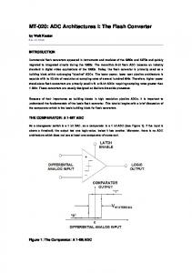
4. Comparator The comparator circuit shown in Figure 3 includes a preamplifier, regeneration circuit and a latch. There are two clock signals to control the amplification and reset of the comparator. The two clock signals are approximately 180 degrees out of phase as shown in Figure 4. The small time space φ, between amplification and reset period is to give the input regeneration stage more time to amplify the signal so as to reduce the delay.
Figure 3: Comparator circuit used in Analog-to-Digital Converter The latch then changes the return-to-zero signal to nonreturn-to-zero signal. During reset, transistor M1 turns on and forces the voltage levels on the two sides to be equal. The next amplification cycle can start after reset by turning off transistor M1. To reduce the offset, the layout of the comparator should be drawn as symmetrically as possible. The comparator of Figure 3, offers an important property that makes it attractive for high-speed design, the static power dissipation is zero.
signal equal to that of the input signal, making it ready for another stage, if higher resolution was necessary.
φ nclk clk Reset
Amplify
Figure 4: Clock signal for the comparator
5. Results The results of the Pipeline block are displayed in a systematic order. Figure 5 first shows the input voltage, marked by ‘A’ in Figure 1. Secondly, the input clock waveform is displayed. Thirdly, the 3-bit output starting with the MSB on top is shown, marked as ‘B’ in Figure 1. The residue output is obtained by amplifying the signal by a factor of 2N. This makes the amplitude of the output
Figure 5: Pipeline ADC outputs When the operating frequency of the analog to digital converter is increased, the dynamic power consumption increases proportionally to the frequency, as illustrated in Figure 6.
6. Conclusion A 3-bit, single-stage CMOS Pipeline ADC that uses a modified flash ADC has been presented, which requires only 2N-1 comparators to implement an n-bit modified flash ADC. This approach greatly reduces the complexity of the flash ADC. Depending on the application, a higher resolution ADC could be obtained by cascading a certain number of three-bit blocks. The Pipeline ADC dissipates 2.893 milliwatts of power, and operates at a maximum speed of 80 MHz.
7. References Figure 6: Power Analysis of the Pipeline ADC The measured performance of the overall 3-bit Pipeline ADC and the associated components within the Pipeline ADC have been summarised in Table 2.
[1]
[2]
Table 2. Summary of the ADC Performance Description
Comp
DAC
3-bit Modify Flash
3-bit Pipeline
No. of devices NMOS PMOS Resistors
9 11
2 4 4
42 40 6
48 44 10
305.623 µW 140 MHz
64.51 µW
3-bits
0.998 mW 135 MHz 3-bits
2.893 mW 80 MHz 3-bits
2V
2V
2V
Power Dissipation Speed Resolution Voltage Supply
2V
[3]
[4]
A. M. Abo, P. R. Gray, “A 1.5-V, 10-bit, 14.3MS/s CMOS Pipeline Analog-to-Digital Converter,” IEEE Journal of Solid State Circuits, vol. 34, 1999, pp. 599-606. I. E. Opris, L. Lewicki, B. Wong, “A SingleEnded 12b 20M Sample/s Self Calibrating Pipeline A/D Converter,” IEEE Journal of Solid State Circuits, vol. 33, 1998, pp. 1898-1903. F. Maloberti, “High Speed Data Converters and New Telecommunication Needs,” Conference Proceeding IEEE, Tucson Arizona, 1999, pp. 147150. A. Stojcevski, J. Singh, A. Zayegh, “Performance Analysis of a CMOS Analog to Digital Converter for Wireless Telecommunications,” Conference Proceedings IEEE, ISIC-2001, Devices & Systems, Marina Mandarin, Singapore, pp. 59-62, 2001.