2015 International Conference on VLSI Systems, Architecture, Technology and Applications (VLSI-SATA)
Design of Ultra Low Power Flash ADC using TMCC & Bit Referenced Encoder in 180nm Technology Aditi Kar
Alak Majumder; Abir Jyoti MandaI; Nikhil Mishra
Department of ETCE Tripura Institute of Technology, Agartala Tripura, India - 799009
[email protected]
Department of ECE National Institute of Technology, Arunachal Pradesh Yupia, India - 791112
[email protected]
Abstract-
Analog-to-digital converters (ADCs) are needed in all those applications, which interface with the analogue world and exploit the digital processing of data. As digital processing is more and more gaining ground over analogue signal processing, the importance of ADCs correspondingly increases. The Flash type ADC, also known as Direct Conversion ADC, uses a bank of comparators, operating in parallel to achieve a high data conversion rate. In this paper, an area efficient low power high Speed 3-bit Flash Type ADC using bit referenced encoder is proposed in 180 nm CMOS technology. The concept of Threshold Modified Comparator Circuit (TMCC) is also introduced as a modification of the conventional comparator. The proposed design of the ADC occupies an active area of 0.0036 mm2 and consumes 43.146 �W of average power while operating with an input frequency (fin) of 10 MHz and a supply voltage of 1.8 Volt. Index
Terms - Flash Type ADC, Comparator, TMCC, Threshold voltage, Multiplexer, Bit referenced encoder
I. INTRODUCTION
VREF
Vdd
Analog circuits are often used in more power constrained situations. Microprocessor and SoC designs may encounter thermal limits of power dissipation or have low power targets for use in 'Green' products. The power consumption of digital CMOS logic is proportional to the square inverse of scaling factor (k) [2]. Digital Power CI) k -2
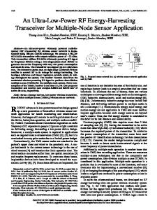
significantly from random mismatch. Each of the comparators operating in parallel has its own random offset resulting from random mismatches between comparators. The random offset creates non-linearity in the ADC transfer function, thereby distorting the output. Control of comparator random offset is essential to create accurate flash ADC. A conventional flash type ADC is shown is figure 1. The series connected resistors are working as voltage divider network thereby consuming a huge amount of static power. Also the no. of used components of a Flash Type ADC increases as resolution increases [I, 5]. The conventional Flash ADC uses comparator composed of uncompensated operational amplifier having large number of transistors leading to large area and huge power dissipation.
8 line to 3 line
Priority
I
I
Encoder
}
.,",,,,0",,,"'
(1)
However, analog power of CMOS flash ADC scales with the inverse of scaling factor when bandwidth is held constant [3]. Analog Power CI) k-
1
(2)
The digital power scales faster than the analog power as the CMOS technology advances, making the increasingly attractive use of digital logic to reduce analog complexity. This has lead to a great deal of research on digital techniques to improve the performance of simple, low resolution analog circuits in ADCs, resulting in 'Mostly Digital' analog circuits [4]. As the comparators used in architecture are in parallel, the flash architecture is a better option for high speed operation, but in terms of power consumption issues it is not that much of efficient. If we talk about latency, flash type ADC is the most appropriate candidate. Flash ADCs in particular suffer
978-1-4799-7926-4115/$31.00©2015 IEEE
Figure 1: Architecture of the Conventional Flash Type ADC
II. RELATED WORK High speed, low power, lower chip area, low aperture jitter etc. are the important parameters by means of which performance of an ADC is analyzed. Among these, low power dissipation is one of the main threats for the researchers. Power dissipation occurs mainly because Transistor Matching, Device Parasitic and Calibration of Designed ADC. The TIQ technique has been used thereby replacing resistor bank of conventional method to design a flash ADC [6]. A capacitive interpolation technique has been used to have a low
2015 International Conference on VLSI Systems, Architecture, Technology and Applications (VLSI-SATA)
power design [7]. In 2002 an average termination circuit is proposed to reduce the number of over-range amplifiers thereby reducing the power consumption [9]. An ADC is designed for disk-drive read channel applications [10]. A new technique named current interpolating technique is implemented to design an ADC operating at IV power supply [II]. In another edition, the authors have addressed the problem of meta-stability, which becomes important when operating at high sampling speed. They proposed a gray encoded ROM as the solution [12]. In the year 2006, it has been shown that the static nonlinearity presents in the track and hold circuit [13] can be reduced. In 2004, a complementary average value technique was proposed in which the input signal is pre-processed before comparing it with a fixed voltage reference level in order to simplify the comparator design [14]. In 2012, a 4-bit asynchronous binary search based ADC has been presented so as to obtain high speed applications [15]. In our proposed architecture, to reduce the area and power dissipation TMCC & Bit Referenced Encoder is employed. III. BLOCKS OF THE PROPOSED ADC A. TMCC
Reduction of the delay and the power consumption can be done by replacing the series combination of resistors and Comparator with TMCCs. The full form of TMCC is Threshold Modified Comparator Circuit. It is basically a buffer circuit having an inverter with modified threshold voltage followed by a NOT gate as shown in Fig. 2.
out
gnd
Figure 2: Circuit of the TMCC
As per required reference voltage we can change the width length ratio (W/L) of the MOS transistors used in the inverter circuit so as to get the modified threshold voltage. The relation between threshold voltage and the aspect ratio can be found from the following equation -
From the above equation, we can find the threshold voltage for each and every TMCC by changing the values of width and length of NMOS and PMOS separately. The following Table I shows different values of width and length of NMOS and PMOS to have different threshold values. Table I TMCC witb various threshold voltages
SL No
TMCC
WN
(Volt)
1 2 3 4 5 6 7
(/.lm) 20 12 1 0.42 0.42 0.42 0.42
0.225 0.450 0.675 0.900 1.125 1.350 1.575
1st 2nd 3rd 4th 5th 6th 7th
PMOS
NMOS
VTH
Wp
LN
Lp
(/.lm) 0.5 0.5 0.42 2 3 15 30
(/.lm) 0.3 0.3 0.18 0.18 1 10 20
(/.lm) 10 1 0.18 0.18 0.18 0.18 0.18
For an inverter present in TMCC when the input voltage is less than threshold (reference) voltage the pull-up transistor is ON and pull-down transistor will be OFF thereby providing a high output considered as 'Logic 1' . But when the input is more than threshold, pull-down transistor will come into ON state thereby giving a low output interpreted as 'Logic 0' . If we focus the operation phenomena of a comparator we can sense that it is quite opposite to that of a comparator. Here, in TMCC we have cascaded one NOT gate with the inverter to have the convention of a comparator. The main advantage of inclusion of NOT gate serves the purpose of logic restoration of the output of an inverter circuit. B. Bit Reference ENCODER
After the comparison of analog input voltage with different reference voltages TMCCs produce a set of data which cannot be used in their original form. To get rid of this problem encoder circuits are designed which makes those data understandable. We introduced Bit Referenced encoder circuit in our proposed ADC architecture. Let 0" O2 ... ...... 07 are the outputs from the TMCCs and D,. D2 & D3 are the final ADC outputs. The expected outputs of the proposed ADC are shown in Table II. Table II
Vth
=
Vto,n+J�/Vdd+Vto,P) (1+v'Kr) 1
Where, Kn
K
p
=
=
fln Cox
fl
Cox p
And the transconductance ratio,
(�)
(�)
n
P
Outputs of the TMCCs and the final ADC Output
(3)
Output of TMCC
Output of AOC
01
O2
03
04
05
06
07
01
O2
03
0
0
0
0
0
0
0
0
0
0
0
0
0
0
0
0
0
0
0
0
0
0
0
0
0
0
0
0 0
0
2015 International Conference on VLSI Systems, Architecture, Technology and Applications (VLSI-SATA)
o
o
o
o
o
o
o
Table II shows the full operation of proposed ADC and how digital bits are generated in the output of Bit Referenced Encoder. The schematic of Proposed Flash type ADC is shown in figure 5, which is designed in CADENCE using 180 nm technology.
o
o
o
From the above truth table we can describe the fundamental operation of our proposed Bit Referenced Encoder. When 04 = 0, 06 = 0 & 07 = 0; Output = 000 04 = 0, 06 = 0 & 07 = 1; Output = 00I 04 = 0, 06 = I & Os = 0; Output = 010 04 = 0, 06 = I & Os = 1; Output = ° II When 04 = 1, O2= 0 & 03 = 0; Output = 100 04 = 1, O2 = 0 & 03 = 1; Output = 101 04 = 1, O2 = 1 & 01 = 0; Output = 110 04 = 1, O2 = 1 & 01 = 1; Output = III From the above analysis we can say that the Bit Referenced Encoder can be implemented using one 2: I Multiplexer followed by one 4: I Multiplexer. The block diagram of it is shown in figure 3. 07 2· : 1 !\olUX 02 -------1
Figure 5: Schematic diagram of Proposed Flash type ADC
05
out
4 :1 !\olUX
03
The analog input is compared with 7 different referenced voltages of TMCCs. Then the outputs are converted into digital form by the Bit Referenced Encoder. Thus an analog signal is converted into digital signal by our proposed Flash type ADC.
04
IV. RESULTS AND DISCUSSIONS
Figure 3: Block diagram of Bit Reference Encoder
2: 1 & 4: 1 Multiplexers are designed in Transmission Gate technology so as to reduce the size of the circuit thereby reducing area and power consumption. As a result the area of the designed Bit Referenced Encoder is also reduced. C. PROPOSED FLASH TYPE ADC ARCHITECTURE
Our proposed Flash type ADC is designed using 7TMCCs and Bit Referenced Encoder. Fig 4 shows the block diagram of our proposed Flash type ADC.
We have designed a 3 bit Flash type ADC using 7 TMCCs and Bit Referenced Encoder. From table-I we see the output of ADC is producing 001,010,011,100,101,110,111. Now as we use 1.8v in cadence for our proposed ADC, we divide 1.8v into 8 different voltages each division will be of 0.225v. Figure 6 shows the input output waveforms of our proposed ADC for a sine wave of 10MHz. when input voltage is 0.225v output of ADC produces 001 and so on. Thus input analog voltage is converted into digital form. O.OOE"'OOO 2_0
VDD
n..
,
..
,
0
"'-" -0 ?O
IN
Bit Referenoed Encoder
J
D
DI D.
.. =
"
�g
=
t' d
=
, ..
I>:2
'
IlL"
.5
-0 ?O
�
:0.3
'
0
"'-"
L...,-I ;::::
f---J I� If---J
----'
-
=
'--
6.00E-ooe T:i-r.n.. eo( s )
Figure 6: Input Output waveforms of the Proposed ADC for a Sine Wave of lOMHz
Figure 4: Block diagram of proposed Flash type ADC
r---'
0
O.OOE . 000
GN D
�
"
',0
:OJ!.
.a-
0
v--
-
'-
2015 International Conference on VLSI Systems, Architecture, Technology and Applications (VLSI-SATA)
A comparative analysis has been done between proposed and previously available ADCs based on some important parameter like Area and Power. The analysis gives a clear message to show that our proposed ADC is using very less area and power as compared to the other existing ADCs. Hence, the proposed method can be preferred for its simplicity in design.
Figure 7 and Figure 8 illustrate different measured DNL and INL values for the proposed ADC structure.
0.1 ,----0.05 +-----'It"----
Table-III shows the comparative study of different design style. Table III
.§
Comparison of different design styles for low power ADCs
---'�--------l'_--
-(L O S +-
______
Design
Proposed
Conventional
Wong
ADC
ADC
Chen
Style
ISSCC
[17]
Architectu
Flash
Flash
Flash
BS
-0.15 +------\-
3-bit 1.8 V
3-bit 1.8 V
6-bit 1.2 V
5-bit 0.8 V
-0.2 -'------
43.146 flW 0.0036
2397.6 flW 0.02075
5.3 mW 0.06
0.5 mW
180
180
130
65
-+-Series1
-0.1 +-------\-
[16] re Resolution Supply Voltage Average Power Area
2 (mm ) Technology (nrn)
code Figure 7: DNL curve of Flash type ADC using TMCC and Bit
0.015
Referenced Encoder
0.09 0.08
A. DIFFERENTAL NON-LINEARITY & INTEGRAL NON
0.07
LINEARITY
Differential Non-Linearity (DNL) is the difference between the ideal and actual input code width, whereas Integral Non Linearity (INL) is the maximum deviation of the transfer function from the straight line between two points along the input-output transfer curve. Expressions for DNL and INL can be written as,
DNL
=
1,
For all 0