Department of Electrical and Computer Engineering,. University of ..... He obtained his Ph.D. and M.S. degrees in Electrical Engineering from Wayne State.
Design Optimization of MEMS Comb Accelerometer Kanchan Sharma, Isaac G. Macwan, Linfeng Zhang, Lawrence Hmurcik, Xingguo Xiong Department of Electrical and Computer Engineering, University of Bridgeport, Bridgeport, CT 06604 Abstract MEMS (Microelectromechanical Systems) refers to the technology integrating electrical and mechanical components with feature size of 1~1000 microns. MEMS comb accelerometers have been successfully applied for air-bag deployment systems in automobiles. In this paper, the design optimization of a polysilicon surface-micromachined MEMS comb accelerometer is discussed. The device uses folded-beam structure to enhance the sensitivity. The movable mass is connected to two anchors through folded-beams. There are movable fingers extruding from both sides of movable mass. Each movable finger has left and right fixed comb fingers surrounding it, so that a differential capacitance pair is formed. Any acceleration along the sensitive direction will induce inertial force on movable mass and deflect the beams. Hence the differential capacitance gap will change. By measuring this differential capacitance change, the experienced acceleration can be measured. ANSYS FEM simulation is used to extract the device sensitivity and resonant frequency of the device. By gradually varying the design parameters in ANSYS simulation, the relationship between the device sensitivity and various design parameters is derived. The curves of device sensitivity versus beam width, beam length and mass width are derived and they are in good agreement with theoretical prediction. From the analysis it is concluded that the device behavior strongly depends upon various design parameters. By adjusting design parameters, desired sensitivity can be obtained. Based on the simulation results, a set of optimized design parameters for the comb accelerometer is decided. The ANSYS simulation results show that the device has displacement sensitivity of 3nm/g. The above-proposed MEMS comb accelerometer may be used for many applications, such as automobile airbag deployment and navigations, fabrication sequence of the comb accelerometer is also proposed. The device is to be fabricated using surface-micro machining process with sacrificial layer technique. I. Introduction MEMS accelerometers are used to sense the acceleration experienced by a system. They have been good examples for MEMS commercial products and have made their way into most of our daily lives [1]-[3]. The most common uses for MEMS accelerometers are in airbag deployment systems for modern automobiles. In this case accelerometers are used to sense negative acceleration of the vehicle. A processor will analyze the magnitude of the acceleration and decide on whether or not to deploy the airbags in the vehicle. MEMS accelerometers are quickly replacing conventional accelerometers for airbag deployment systems in automobiles. The reason behind this increasing popularity is, the MEMS accelerometers are much smaller, lighter, more reliable and are produced for a fraction of the cost of the conventional bulky accelerometers. Several new innovations in micromachining have been combined to make a commercially available accelerometer for low g (gravity acceleration) applications. One of the successful innovations is straight beam comb accelerometer. The straight beam is anchored at four points. While this sensor is stiff and robust, it is also sensitive to mechanical stress imparted to the die from the package and die amount. The recent innovation of Analog devices Inc. ADXL50 is folded beam comb accelerometer [4]. The folded beam structure is anchored only at two points. The wrap around structure relieves the tension of poly-silicon which makes the beam much less sensitive to package stress. At the same time, the compliance of beam, i.e. the deflection of beam for a given acceleration applied, is increased which enhances the sensitivity. In addition to accelerometers, many other MEMS devices such
1
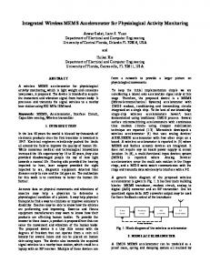
as MEMS gyroscopes, digital micromirrors, MEMS optical switches, DNA chips, have been successfully developed and commercialized [5]. MEMS, together with nanotechnology, are believed to be the drive to trigger the next wave of technology revolution. As MEMS technology continue to grow, MEMS device design optimization is becoming an interesting and important research issue. In order to design a MEMS device to meet the given specifications, the relationship between the device performance and various design parameters must be investigated. Various efforts on MEMS device design optimization and automation have been made. For example, in [6], the design optimization and simulation on a microelectromagnetic pump was discussed. In [7], the mechanical design and optimization of a capacitive micromachined switch was proposed. In [8], an automated approach is used to generating novel MEMS accelerometer configurations. Considering the commercial success of MEMS accelerometers, the design optimization of a folded-beam MEMS comb accelerometer device is discussed in this paper. The relationship between the device sensitivity and the design parameters (such as beam width, beam length, mass width) is analyzed. ANSYS FEM simulation [9] is used to derive the device sensitivity for various design options. Based on the analysis, an optimized design of the MEMS comb accelerometer device is suggested. II. Device Design The structure design of a poly-silicon surface-micromachined MEMS comb accelerometer is shown in Figure 1. This device is similar as ADXL 150 accelerometer [4] developed by Analog Devices Inc.
Figure 1. Structure diagram of folded-beam accelerometer
The movable parts of this MEMS comb accelerometer consist of four folded-beams, a proof mass and some movable fingers. The fixed parts include two anchors and some left/right fixed
2
fingers. The central movable mass is connected to both anchors through four folded beams. There are many movable fingers extruding from the both sides of the central mass. In the right and left side of the each movable finger, there are left and right fixed fingers. The movable fingers constitute the differential capacitance pair C1 and C2 with left and right comb fingers. When there is no acceleration, the movable fingers are resting in the middle of the left and right fixed fingers. In this way, the left and right capacitance pairs C1 and C2 are equal. If there is any acceleration a along horizontal direction parallel to the device plan, the proof mass Ms experiences an inertial force -Ms·a along the opposite direction. As a result, the beams deflect and the movable mass and movable fingers move for a certain displacement x along the direction of the inertial force. The left and right capacitance gaps are changed, hence the differential capacitances C1 and C2 will also be changed. By measuring this small differential capacitance change, we know the value and the direction of the experienced acceleration. This is the working principle of the MEMS comb accelerometer. The comb accelerometer design also supports in-field builtin self-test feature. Among these capacitance pairs, most capacitance groups act as the sensing capacitance and other few capacitance groups act as built-in self-test capacitance. The built-in self-test feature allows the device to be self-tested during in-field usage using electrostatic force. In test mode, when there is no acceleration, a driving voltage Vd is applied to the left or right fixed driving fingers. The electrostatic force will attract the movable fingers toward the left or right direction. By measuring this displacement and comparing with good device response, one knows whether the device is good or faulty [4]. This self-test feature is especially important for the safety critical applications such as automobile airbag deployment.
III. Performance Analysis of the Device When an acceleration a along the horizontal direction parallel to the device plan is applied to the accelerometer, the beam deflects under the effect of inertial force. The deflection of beam is in opposite direction of the applied acceleration. The displacement sensitivity of the device is defined as the displacement of the movable mass (and movable fingers) per unit gravity acceleration g (1g=9.8m/s2) along devices sensitive direction. The beam-mass structure of the accelerometer can be treated as a simplified spring-mass model. The four folded-beam can be treated as four springs connected in parallel. For each folded-beam, both sections of the beam can be treated as two springs connected in series. Each beam section can be treated as double-clamped beam model. Assume for each section of the folded-beam, the beam width and length are Wb and Lb separately. The width and length of central proof mass are Wm and Lm separately. The device thickness (thickness of the poly-silicon layer) is t. There are totally Nf finger groups, among which there are Ns sensing finger groups and Nd driving finger groups (Nf=Ns+Nd). For each movable finger, the finger width and length are Wf and Lf separately. When there is no acceleration, the capacitance gap between each movable finger and its left (right) fixed fingers is d0. The density ρ and Young’s modulus E of poly-silicon material are given as below. The density of poly-Si is ρ = 2.33 × 10 3 kg / m 3 Young’s modulus of poly-Si is E=1.70×10¹¹Pa When there is no acceleration, the static sensing capacitance of the MEMS comb accelerometer is
C10 = C20 = C0 =
ε ⋅ Ns ⋅ Lf ⋅ t d0
(1)
where ε is the dielectric constant of air.
3
Assume there is acceleration along left direction horizontally, the movable mass experiences an inertial force toward right by x, as shown in Figure 2. Assume small deflection approximation (x