966
IEEE TRANSACTIONS ON ELECTRON DEVICES, VOL. 48, NO. 5, MAY 2001
A TCAD Approach to the Physics-Based Modeling of Frequency Conversion and Noise in Semiconductor Devices Under Large-Signal Forced Operation Fabrizio Bonani, Member, IEEE, Simona Donati Guerrieri, Member, IEEE, Giovanni Ghione, Senior Member, IEEE, and Marco Pirola, Member, IEEE
Abstract—The paper presents a novel, unified technique to evaluate, through physics-based modeling, the frequency conversion and noise behavior of semiconductor devices operating in large-signal periodic regime. Starting from the harmonic balance (HB) solution of the spatially discretized physics-based model under (quasi) periodic forced operation, frequency conversion at the device ports in the presence of additional input tones is simulated by application of the small-signal large-signal network approach to the model. Noise analysis under large-signal operation readily follows as a direct extension of classical approaches by application of the frequency conversion principle to the modulated microscopic noise sources and to the propagation of these to the external device terminals through a Green’s function technique. An efficient numerical implementation is discussed within the framework of a drift-diffusion model and some examples are finally provided on the conversion and noise behavior of rf Si diodes. Index Terms—Microwave devices, nonlinear systems, semiconductor device modeling, semiconductor device noise, sensitivity.
I. INTRODUCTION
R
ECENTLY, great interest has been placed on the modeling and simulation of electron devices operated in large-signal conditions (LS). Such regime is particularly important in classical analog radio-frequency (rf) applications, either quasilinear, such as power amplifiers, or nonlinear, such as mixers and frequency multipliers. Owing to the increasing importance of silicon-based analog rf applications, a growing attention exists on the development of technology computer aided design (TCAD) tools able to analyze and optimize the LS device behavior [1], [2]. During the last few years, LS analysis techniques for analog circuit simulation such as the harmonic balance (HB) method [3]–[5] have been successfully applied to the LS physics-based numerical device modeling, see [6], [1], [7], [8]. However, further techniques, that have been developed in the field of circuit simulation, are relevant to the physics-based analysis of devices operating in the LS regime. A first example concerns the analysis of frequency conversion in the presence of multi-tone inputs, which has paramount importance in simulating e.g., mixer operation or the intermodManuscript received June 28, 2000; revised October 16, 2000. The review of this paper was arranged by Editor J. N. Hollenhorst. F. Bonani is with the Dipartimento di Elettronica and INFM Unità Torino Politecnico, Politecnico di Torino, 10129 Torino, Italy (e-mail:
[email protected]). S. D. Guerrieri, G. Ghione, and M. Pirola are with the Dipartimento di Elettronica, Politecnico di Torino, 10129 Torino, Italy. Publisher Item Identifier S 0018-9383(01)02371-1.
ulation behavior of power amplifiers. Although the HB method can generally handle this case, the computational intensity of the solution is greatly increased. A useful approximation to frequency conversion in the presence of a strong input tone (such as a local oscillator) superimposed to one or more weak input tones (such a signal to be up- or down-converted) is provided by the so-called small-signal large-signal (SS–LS) analysis [9], which implies the model linearization around the instantaneous working point. SS–LS analysis provides a linear relationship between the (weak) input tone amplitude and the output tone resulting from frequency conversion through the so-called conversion matrix [9]. A second example is noise analysis under LS operation. As well known from circuit theory (see, e.g., [5] and [10]) noise and SS–LS analyses are strictly related, since noise can be interpreted as a small, random perturbation affecting a system operating in a steady-state LS regime. Induced noise therefore results as the frequency conversion of noise sources, which, owing to the periodic nature of the instantaneous working point, already experience amplitude modulation (and therefore frequency conversion) with respect to the conventional small-signal case. A comprehensive approach for the LS noise analysis of both nonautonomous and autonomous (self-oscillating) circuits has been presented in [10]; many of the theory keypoints, such as the use of modulated noise sources and the related noise frequency conversion, were already found in the pioneering paper [11]. The present paper focuses on the extension of the TCAD approaches to the analysis of frequency conversion and noise in LS operation. In particular, we propose a unified treatment of the two, which generalizes, as far as noise analysis is concerned, the Green’s function approach proposed by some of the present authors [12]. The Harmonic Balance technique is applied to the discretized physics-based model to determine the LS steadystate solution, and a generalization of the circuit SS–LS HB analysis is exploited to determine, from physics-based models, the device conversion matrix. Concerning physics-based noise analysis, a first modeling technique was proposed in [13], extending the so-called active line approach [14]. The present approach directly generalizes the classical Green’s function approach [12] and the related impedance field method (IFM) [15], allowing for the direct evaluation of the device noise sideband correlation matrix [16], which yields the power and correlation spectra of the noise spectral components at the device terminals resulting from the frequency conversion process, see Section II.
0018–9383/01$10.00 © 2001 IEEE
BONANI et al.: PHYSICS-BASED MODELING OF FREQUENCY CONVERSION
967
The paper is structured as follows. Section II presents an outline of the frequency conversion and noise theory mainly from a system standpoint, and is intended to provide the basis for further discussion and application to physics-based modeling. Section III briefly reviews the LS formulation and introduces the SS–LS analysis through model linearization around the instantaneous working point. The LS noise analysis formulation is discussed in Section IV. Finally, implementation issues, including some computational aspects, and examples of application are presented in Section V, where the results of the physics-based model are compared and found to be in good agreement with conventional equivalent circuit analysis.
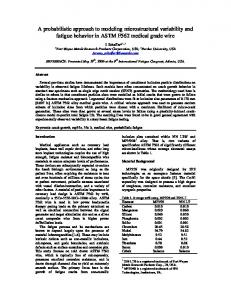
II. OUTLINE OF FREQUENCY-CONVERSION AND NOISE THEORY IN LS OPERATION As well known, in the forced LS regime the device is excited by a large electrical input signal generally made of a superposition of harmonic components or tones. According to the application of interest, the device is driven into a mildly nonlinear regime (as in power amplifiers) or into full nonlinearity (as in mixers and frequency multipliers); in all cases, nonlinearity results in the generation of harmonics and intermodulation products. Simple, though practically important cases, are the single-tone input and the two-tone input cases. In the former, the input signal is strictly periodic with (angular) frequency ; device , nonlinearity produces signals with spectrum integer. In the latter, the input frequency components are and , and the resulting spectrum is the set , and integers. The operation is termed quasiperiodic when the input frequencies are incommensurate, i.e., their ratio is not a rational number; extension to the multi-tone regime is straightforward. From an application standpoint, an important case occurs when two input tones are present, one strong, the other weak. In this case, the small-amplitude (weak) signal at frequency is superimposed to the LS (strong) input at , thus linearly perturbing the LS regime. Linearization around the LS working point is the object of the small-signal large-signal (SS–LS) analysis [9]. In this case, the output spectrum results as the set , where is the unperturbed LS spectrum, with the is converted following interpretation: the input frequency into an output set of spectral lines, usually referred to as sidebands, symmetrically placed with respect to each harmonic of the unperturbed LS regime (see Fig. 1). Due to linearity, the amplitude of the output sidebands is proportional to the amplitude of the (weak) input. This concept can be generalized if the weak input signal spectrum is already made of sidebands ; the same spectrum is found at the output, and the linear relation between the input and output sideband amplitudes can be represented by means of the so-called conversion matrix (CM). Notice that the CM is, in general, not diagonal, thus implying frequency conversion between each input and output sideband. To formally derive the concept of frequency conversion within a system framework, let us consider a nonlinear system having a periodic input with fundamental frequency . The
Fig. 1. Frequency conversion in a nonlinear system driven by a single tone LS excitation and a small-amplitude signal.
system output has a frequency spectrum composed of all the harmonics of the input frequency integer
(1)
and can be therefore expanded into a Fourier series. Consider now the case wherein a small-amplitude signal is superimposed to the system input, resulting in a perturbation of the LS periodic steady-state. The system response can be obtained by SS–LS analysis [9], i.e., through linearization around the LS solution, yielding a linear periodically time-varying (LPTV) system. A general theory of LPTV systems, based on the transfer function formalism, is beyond the scope of this paper, and can be found, e.g., in [17]. For the sake of our discussion, we confine the treatment to the simple case of a LPTV system defined by (2) is a forcing term (the input), and is a periodic where function corresponding to the memoryless part of the system:
(3) is a real function of time, for any . Since According to SS–LS theory, the input (and therefore the output) signal spectra are the set of sideband frequencies (4) where the refers to the upper sideband and the to the lower sideband, displaced by an amount from the central frequency (see Fig. 1). For instance, the Fourier expansion of the output signal is
(5)
968
where and conditions allow to express time varying function:
IEEE TRANSACTIONS ON ELECTRON DEVICES, VOL. 48, NO. 5, MAY 2001
. These symmetry as the real part of the complex
(6) sufficient to characthus making the set of coefficients terize the waveform in (5). Similar expressions hold for the input . Notice that, hereafter, capital variables will always denote the frequency components of the corresponding time-domain quantities. Introducing into (2) the complex signals and the expansion are readily shown to satisfy (3), the sideband amplitudes the infinite algebraic linear system (7) The inverse of the coefficient matrix of such infinite set of equations is the conversion matrix of the LPTV linear system. By collecting the sideband amplitudes into infinite vectors, one has (8) where we have explicitly stated the dependency of the CM on the displacement frequency , which results from the memory part of the LPTV system. Suitable truncation must be performed on the spectra and on the CM to make the problem practically manageable. The CM approach (8) can be shown to apply to a generic LPTV system, see, e.g., [9] on the evaluation of for a lumped-parameter network operating in the SS–LS regime. The CM formalism is also the basis of LS noise analysis. As a first step, noise sources are amplitude-modulated by the periodic LS steady-state [11]; this process is equivalent to the passage of the stationary random process describing noise sources in dc conditions through a memoryless LPTV system of periodicity , thus implying noise frequency conversion into a sideband (see also Section IV). Modulated noise sources can set be characterized in terms of a cyclostationary random process [5], [17], [16], whose spectral representation is provided by the power and correlation spectra of its sideband components. It can be shown that sideband noise spectral components at and are uncorrelated unless (see Fig. 2); therefore, the noise spectral representation is reduced to the so-called sideband correlation matrix (SCM) , which generally depends on and whose diagonal components are the sideband power spectra. As a second step, the cyclostationary amplitude-modulated and frequency-converted (sideband) fluctuations can be interpreted as small-amplitude perturbations of the LS steady-state; therefore, the resulting output fluctuations can be analyzed through the SS–LS approach. This second frequency converresults sion through a LPTV system of the same periodicity again in a cyclostationary process [17], and the relationship between the input and output SCM is easily derived by (8): (9)
Fig. 2. Correlated noise sidebands.
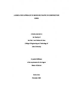
From a circuit standpoint, the CM and noise SCM are the basis for the so-called multifrequency representation of a noisy -port [9], generalizing the small-signal Norton or Thevenin equivalent circuits to the SS–LS regime. Consider in fact a noisy -port operating in LS periodic conditions, and suppose to add a weak perturbation whose spectrum belongs to the sideband spectrum of the LS steady-state, with sideband frequency . The sideband amplitudes of port voltages and currents will be related by the Norton representation (10) is the sideband shortwhere is the admittance CM and circuit (s.c.) current fluctuation vector described by the SCM . Similarly, one has the Thevenin representation (11) is a sideband openwhere is the impedance CM and circuit (o.c.) voltage fluctuation vector described by the SCM ; the open- and short-circuit fluctuation SCM’s are related as (12) Formally, each port of the multifrequency, multiport representation corresponds to a different sideband; as an example, Fig. 3 shows the relevant parallel representation for a two-port, where the input and output ports are expanded into a set of sideband ports. Notice that the multifrequency, multiport model, exactly as the small-signal noisy model, provides both the small-signal response to an external sideband excitation, and the noise superimposed to it. In particular, in the absence of the external excitation, it enables to evaluate, once that the model is embedded into an external circuit, the noise spectrum in LS operation. The model therefore provides a complete noise characterization in the LS regime, and a full signal and noise characterization in the SS–LS regime. In the following sections, a physics-based evaluation of the multifrequency model will be developed, exploiting the concepts of frequency conversion of deterministic and random signals. III. LARGE-SIGNAL AND SS–LS ANALYSIS In the following discussion, attention will be focused on a simple bipolar drift-diffusion (DD) model, consisting of Poisson’s equation and of the electron and hole continuity equations, see e.g., [18]. Although the limitations of the DD approach in the modeling of submicron devices are well known,
BONANI et al.: PHYSICS-BASED MODELING OF FREQUENCY CONVERSION
969
where , and , , denote the discretized Poisson, electron continuity and hole continuity equations, respectively. Discretization of the boundary conditions on the equations external, contact nodes leads to the (13d) (13e) (13f)
Fig. 3.
which, in order, denote the boundary conditions relative to the Poisson and continuity equations. Boundary conditions on the noncontact device boundaries are already included in the equations for the internal nodes.1 Finally, equations are further needed to close the unknowns. Such equasystem in the tions express the contact currents as a function of the nodal unknowns
Multifrequency representation of noisy two-port.
this technique can provide a first estimate of the device behavior. The extension of the approach proposed to higher-order transport models is in principle straightforward as far as the Green’s function evaluation is concerned, though in practice extremely intensive from a computational standpoint. However, one has to consider that the modeling of the microscopic noise sources within a full hydrodynamic model is not completely established yet, see [19] and references therein for further details. We assume that the DD model has been spatially discretized through the so-called finite-boxes approach (see, e.g., [20]) on a suitable grid, thus making the problem unknowns a set of time-domain spatial samples of the electrostatic potential and of the electron and hole densities and . For the sake of this the number of nodes internal to discussion, let us define as the device volume, including those on the external boundaries the number but not pertaining to metallic contacts, and as is, of external, boundary nodes lying on metallic contacts; finally, the number of metallic contacts, ohmic or Schottky, corresponding to the device terminals, excluding the reference contact, which is grounded. Concerning the system unknowns, we ( ) nodal values corredenote with subscript ( ) the sponding to the internal (external) nodes, which will be referred contact voltages and curto as nodal unknowns. Finally, rents , collectively denoted as circuit unknowns, are also exploited. A. LS Analysis Let us discuss first the time-domain equations of the spatially discretized DD system under LS excitation. As well known, the LS regime requires the equations of the embedding circuit to be solved together with the physics-based model [21]. The discretized DD model leads to the following sets of nonlinear, dydisnamic nodal equations. The first corresponds to the cretized equations for the internal nodes (13a) (13b) (13c)
(13g) and the constitutive relationships of the external circuit conungrounded device terminals nected to the (13h) is the set of periodic LS applied (voltage or current) where sources. According to the assumption of periodic LS steady-state, each unknown (nodal and circuit) is made of a superposition of harmonics, and therefore can be expressed according to (14) complex spectral amplitudes correspond where the independent real numbers, since for to any . We stress that such a complex representation is used in the formulation because it is well suited to introducing the SS–LS analysis; from a practical standpoint, a direct (real) Fourier representation is more convenient [21], and the present implementation, discussed in Section V, was made accordingly. Further, notice that the harmonic decomposition has been ; this approximatruncated to a finite number of harmonics tion is justified since, in practical circuits and devices characterized by a global low-pass response, the spectral amplitude finally decreases as the harmonic order grows. For quasi periodic operation, the truncation criteria are more involved than for strictly periodic functions, although the present formulation still holds; for a discussion, see e.g., [21]. The HB method can be applied to solve the nonlinear algebraic system (13a)–(13h) as follows [22]. Let us define a set of time samples distributed in the fundamental period 1Notice that the extension to the energy balance bipolar transport model requires to add the discretized energy transport equations for electrons and holes, and the corresponding boundary conditions, leading to 5 ( + ) equations. For the full hydrodynamic approach, moment conservation equations are further needed, leading to 7 ( + ) discretized equations.
2N
2N
N
N
970
IEEE TRANSACTIONS ON ELECTRON DEVICES, VOL. 48, NO. 5, MAY 2001
, where , and let us consider the collection of the sampled variable values , so that (14) yields (15) is given by
where matrix
.. .
.. .
.. .
.. .
.. .
.. . (16)
The choice of the time samples is often performed so as to make the condition number of matrix as low as possible [22]. In the strictly periodic case, this amounts to choosing equispaced time samples, while for quasiperiodic regime an efficient approach, suitable for large-scale problems, is the frequency remapping technique [21], which enables the use of DFT algorithms for the time-frequency transformation. The time derivative of (14) immediately yields the spectral as , where diag is a dicomponents of . Moreover, given a agonal matrix of dimension , its frequency-domain representamemoryless function where is the collection tion is given by . of time-domain samples of Let us now introduce an expanded frequency-domain unknown vector collecting the frequency components of all node scalar terms and circuit unknowns (i.e., including for each unknown), see Fig. 4. Moreover, scalar functions frequency components are expanded into their as well. According to this notation, system (13a)–(13h) is translated, in the frequency domain, into the following set of algebraic equations
Fig. 4. Expanded vector for the frequency components of vector dynamical equations.
B. SS–LS Analysis In order to introduce the SS–LS analysis, let us apply the equivalence theorem [24] to the external device terminals, so as to replace the circuit equation (13h) with a linear relationship corresponding with equivalent current (or voltage) sources to the terminal currents (or voltages) evaluated in the LS steadystate (18) If we superimpose now a small-amplitude harmonic perturbato the LS steady-state, each model unknown (nodal and tion circuit) can be decomposed as the sum of the LS steady-state so. After lution and a small perturbation : linearization, (13a)–(13h) can be cast into the form
(19a) (19b)
(17a) (17b) (17c) (17d) (17e) (17f)
(19c) (19d) (19e) (19f)
(17g) (17h) and are block diagonal matrices made, respecwhere and replicas of . The solution of the nontively, of linear HB system can be performed by means of Newton or quasi-Newton iteration, see [21] for a discussion of the specific problems arising in device modeling. In particular, large-scale problems, such as those arising in 2-D device simulation, require to exploit iterative techniques for the solution of the linear systems arising in the Newton method; see e.g., [21], [23].
(19g) (19h) where the first factor of each term is the (matrix) gradient of the corresponding model equation evaluated in the LS steadystate. The vector system (19a)–(19h) is analogous to the scalar example of LPTV (2). Notice, however, that Poisson’s equation (and its boundary condition) is memoryless, and that in (19h) the matrices are diagonal, with diagonal elements equal to either 0 or 1. If the equivalent source for terminal is a current
BONANI et al.: PHYSICS-BASED MODELING OF FREQUENCY CONVERSION
971
(voltage) generator, the element of ( ) is 1, and the element of ( ) is zero. According to the procedure outlined in Section II, each unknown is expanded into the sideband formulation (20) . Then, system where in general, as discussed later, (19a)–(19h) is expressed in the spectral domain leading to a conversion matrix formulation akin to (8) Fig. 5. Expanded matrix for the frequency components of function (matrix) gradients.
(21a)
(21b)
(21c) (21d)
(21e)
(21f)
(21g) (21h) in (21a)–(21h) are assembled acThe conversion matrices cording to the following rule, here presented, as an example, for . For each node and for each nodal equation, each eleis converted into frequency domain, ment of the matrix resulting in a CM according to the memoryless part of (7), thus a matrix of matrices, see Fig. 5. For instance, making for node and nodal equation , the elements of the conversion submatrix are: (22) are sideband indices, and is the vector of where . As far as the memory part frequency components of of (19a)–(19h) is concerned, according to the easier example (7) and . we have introduced in (21a)–(21h) the matrices and times, These are block diagonal matrices, replicating diag . respectively, the fundamental matrix To fully account for all the possible conversions among the , the LS solution must be carried sidebands up to the order , see (7). System (21a)–(21h) out to the order is therefore a set of
complex equations, to be compared with the real equations to be solved in the LS case. From a computational standpoint it is also important to emphasize that if a Newton method is used to solve the LS equations, the harmonic component of each element of the matrix gradients in (19a)–(19h), necessary to assemble the conversion matrices as described in (22), are readily evaluated from the Jacobian matrix in the last iteration of the Newton loop [25]. In order to enable evaluating the device terminal CM, the in (21a)–(21h) must include an independent source term excitation for each sideband and each terminal; this implies that is a unit diagonal matrix of dimension . columns corIn the source matrix, each block of responds to the excitation of one device terminal (e.g., terminal ) for every sideband, and the solution of (21a)–(21h) allows to evaluate all the blocks of the device CM corresponding to injection in terminal , i.e., the device conversion submatrices between terminal and every device terminal (see Fig. 6). In particular, the device CM is evaluated when the forcing term is a voltage source, and the CM when the forcing term is a current source. The evaluation of hybrid CM’s is similar. IV. LS PHYSICS-BASED NOISE ANALYSIS The aim of physics-based noise analysis is to evaluate the second order statistical properties of the fluctuations of the terminal electrical variables induced by the fundamental microscopic velocity and carrier number fluctuations that occur inside the device. For LS device operation, this corresponds to the evaluation of the SCM of the equivalent s.c. current (or o.c. voltage, or any set corresponding to hybrid representations) noise generators at the device ports, as shown in Fig. 3. According to the Langevin approach [26], the microscopic noise sources appear as stochastic forcing terms in the right-hand-side of the carrier continuity equations [12], and therefore are homogeneous to a generation-recombination (GR) rate. The basic assumption is that microscopic fluctuations have small amplitude, so that the device response can be evaluated by linearizing the model equations around the noiseless steadystate working point, and thus enabling the conversion matrix formalism to be exploited. Due to linearity, the induced fluctuations at the device terminals can be evaluated by means of a convolution integral of the microscopic fluctuations with suitable Green’s functions of the linearized system, thus extending to the LS case the Green’s function approach in [12], originally
972
IEEE TRANSACTIONS ON ELECTRON DEVICES, VOL. 48, NO. 5, MAY 2001
Fig. 7. Physics-based noise analysis in LS conditions. Fig. 6. Evaluation of the device terminal conversion matrix.
introduced for the noise analysis of devices operating in a stationary (dc) steady-state. The relevant Green’s functions relate a unit injection in the electron or hole continuity equations to the o.c. voltage or s.c. current variations at the device terminals, depending on the boundary conditions enforced on the linearized system. Both microscopic and terminal fluctuations are expressed as sidebands, so that the Green’s functions turn out to be conversion matrices, referred to as conversion Green’s functions (CGF). The physics based noise analysis is therefore carried out in two steps, depicted in Fig. 7. The first consists in assessing the statistical properties of the microscopic noise sources as a result of the time-varying, LS noiseless steady-state. The second step is the propagation of the microscopic noise sources to the device terminals by means of the relevant CGFs, thus expressing the terminal noise SCM according to a generalization of the Green’s function technique for noise analysis in dc regime [12], [15]. The evaluation of the CGF can be carried out by applying SS–LS analysis to the Langevin system.
is often modeled through equivalent current density noise sources [28] with a Lorentzian spectrum, characterized by time constants typically in the range 1 ms 1 s. In this case, the source modulation should be restricted to frequency components of the steady state below the Lorentzian cutoff frequency [29]. The same remark applies for the phenomenological source noise [30]. Such a noise mechanism, exploited to model despite its relevance in LS operated circuits, still lacks a widely noise physics-based accepted physical description, so that analysis would require a careful comparison to measured data (see also the discussion in [29]). Let us consider first velocity fluctuations. These must be expressed in terms of equivalent current density fluctuations, in order to be included as forcing terms for the continuity equa( and ) the tions [26]. Let us define as (spatial) component of the vector current density fluctuation for carrier . The elements of the SCM of the velocity fluctuaand are given by tions for spatial components
(23) A. Microscopic Noise Sources In the first place the statistical properties of the microscopic fluctuations must be evaluated in the LS regime. In our work, we consider two kinds of microscopic fluctuations, namely velocity (diffusion noise) fluctuations and population (GR noise) fluctuations [12]; both fluctuations are assumed to be spatially uncorrelated. Moreover, while hole and electron population fluctuations can be correlated, velocity fluctuations of electrons and holes are physically uncorrelated. In DC steady-state conditions, both are modeled as white processes [26] related to the fast microscopic dynamics of particles, with characteristic times of the order of less than 1 ps. For this reason, such processes can be considered as slowly modulated by the LS instantaneous working point [11], [27] (see Fig. 7). Such an amplitude modulation can be modeled as the passage through a time-varying, memoryless linear system, characterized by a CM independent of the input frequency. Following this, the local noise source becomes a cyclostationary noise process which can be characterized by a SCM, as outlined in Section II, implying that frequency components belonging to different sidebands are correlated only if their frequency deviation from the respective LS frequency is the same. Notice that GR noise
(24) for electrons and holes, respectively. In the previous equations, is the component of the diffusivity tensor for are the frequency the corresponding carrier, and components of the LS electron and hole density distributions. ( Concerning population fluctuations, we indicate as ) the microscopic noise source appearing in the continuity equation for carrier . The SCM of population fluctuations can be obtained by amplitude modulation of the dc expression [28], which depends on the steady-state value of the sum of genera. tion and recombination rates, and will be denoted as B. Terminal Noise Evaluation Through the CGF Approach According to the Langevin formulation and the linearization of the device model around the instantaneous LS working-point, the (sideband) device response is expressed as a function of the relevant Green’s functions, depending on the variable chosen as output. Both contact o.c. voltages or s.c. currents can be sought for. Since microscopic noise sources are distributed within the device volume, the output is expressed through a convolution
BONANI et al.: PHYSICS-BASED MODELING OF FREQUENCY CONVERSION
973
integral whose kernel is the (space-dependent) CGF, thus extending the result (8). For instance, the s.c. current induced at terminal is evaluated with the superposition integral:
(27f)
(27g) (27h) (25) is the where is the device volume, the Green’s function conversion matrix (CGF) for continuity equation and terminal , ( ) is the vector of sideband amplitudes for the ( ), and is the sideband microscopic noise source displacement frequency. Finally, by properly extending (9) the SCM of the s.c. noise currents for terminals and is derived as:
with In (27a)–(27h) we have substituted the unknowns corresponding to a global CGF collecting the CGF’s defined for each terminal; is the Kronecker symbol, expressing that the source is injected either in the electron or in the hole continuity equation, to solve for the electron or hole CGF, respecand correspond to the unit source tively. Source terms terms, homogeneous to an injected current, and are unit diag. Notice that the onal matrices of dimension source term is explicitly placed in the internal nodes of the discretized model only, since injection in a terminal node results in a unit diagonal CGF for that terminal current, and to zero for the other terminal currents. In order to directly evaluate the CGFs, backsubstitutions of one factorization and the linear system (27a)–(27h) are therefore needed, thus making LS noise analysis a formidable task, unless the numerical techniques discussed in the next Section are implemented.
(26) The previous formulation allows to evaluate the global SCM of the s.c. noise current at the device terminals. The CGFs are evaluated from the discretized linear system (21a)–(21h) already introduced for the SS–LS analysis, though for noise analysis the linearized system must be slightly modified. As no external forcing term is applied at the device terminals, (21h) is not needed anymore, while an auxiliary equation must be added to enforce s.c. (o.c.) boundary conditions if the s.c. (o.c.) CGF is sought for. To fix the ideas, we will refer in the following discussion to s.c. boundary conditions. A unit diagonal forcing term, i.e., an independent sideband by sideband excitation, is then added, for each node, to the right-hand-side of each continuity equation, enabling the evaluation of the CGFs. The resulting system of equations is
(27a)
(27b)
(27c) (27d)
(27e)
V. NUMERICAL IMPLEMENTATION AND EXAMPLES We have implemented the LS HB analysis in a two-carrier drift-diffusion model discretized by means of the finite-boxes technique. A mixed-mode approach was exploited, whereby the discretized model is solved together with the equations of the external circuit; solution of the HB system was obtained through Newton iteration. SS–LS and noise analyzes were implemented in the numerical model following the formulation presented in Sections III and IV; however, the evaluation of the CGF’s was not carried out directly (as discussed in Section IV), due to the heavy computational burden corresponding to the backsubstitutions of the linear system (27a)–(27h). Rather, an efficient numerical technique, derived as a straightforward extension of Branin’s approach proposed by some of the present authors in [12] for dc noise analysis, has been ex, allowing for the reduction ploited to compute the unknown of the computational intensity to a number of system backsolves , i.e., the same number of backsolves equal to needed for the evaluation of the terminal device CM by means of SS–LS analysis. As an example of practical application, we have simulated an rf varactor frequency doubler, which can also be exploited to realize a subharmonic mixer. The circuit is shown in Fig. 8; subharmonic mixing can be achieved by injecting an IF signal across the diode terminals (i.e., into node ) through a bandpass filter centered at the IF frequency. The doubler consists of a reverse-biased silicon pn diode connected to a standard external circuit providing input and output matching together with suppression of unwanted harmonics through the idler resonators. The diode cm , length 25 chosen is symmetrical, with a doping level m and area 10 m . The dc and small-signal behavior of the
974
IEEE TRANSACTIONS ON ELECTRON DEVICES, VOL. 48, NO. 5, MAY 2001
Fig. 8. Circuit scheme for the varactor frequency doubler.
diode, simulated by means of the drift-diffusion model, was exploited to extract a standard lumped-parameter LS equivalent circuit model, later used for circuit design by means of the HP MDS simulator. The circuit was optimized assuming as a goal the frequency conversion efficiency from the fundamental (at 1 GHz) to the second harmonic, obtaining a 60% conversion gain at 10 dBm input power. The physics-based HB LS simulation of the diode, embedded into the optimized circuit, was carried out with harmonics (plus dc). 350 grid points and For the sake of the application of the device as a mixer, the diode CM is relevant to predict circuit performance. Some of the elements of the diode admittance CM are shown in Fig. 9 as a function of the sideband frequency; the continuous line are results derived from the conventional LS equivalent circuit, diamonds are derived through SS–LS analysis of the physics-based model. The meaning of the CM elements shown can be explained as follows: out-of-diagonal elements such denote the amount of up-conversion to the second as sideband (i.e., around 2 GHz) experienced by an intermediate frequency (IF) input signal. Diagonal elements such as express on the other hand the current response in the second sideband for an applied voltage at the same absolute frequency; from a circuit standpoint, such elements can be interpreted as the small-signal admittance resulting from the quasistatic diode capacitance averaged on the instantaneous, periodically varying, working point. Since the embedding circuit has been optimized for frequency doubling rather than for IF upconverdenoting conversion from the first to sion, the element . As seen from the second harmonic actually is larger than Fig. 9, excellent agreement exists between the predictions of the physics-based and circuit models. Concerning noise, we evaluated the SCM of the external (s.c. current) diode noise sources and compared it with the results derived from standard circuit LS noise theory, i.e., by generalizing Nyquist theorem according to [11], [17]. The agreement is generally good, and is excellent for the diagonal elements of the SCM shown in Fig. 10. Since in reverse bias the shot-like diode noise is negligible, the varactor diode noise is expected to originate from resistive parasitics, consistent with the increasing frequency behavior shown in Fig. 10 which, from a circuit standpoint, can be derived through a simple series RC circuit where the resistor exhibits thermal noise. This behavior is confirmed, as discussed further on, by the results from physics-based analysis concerning the internal behavior of the diode noise distribution.
Fig. 9. Frequency dependence of the real (top) and imaginary (bottom) part of the elements Y , Y and Y of the varactor admittance conversion matrix. The full line is the result from circuit analysis, the symbols from the physical model.
Fig. 10. Comparison between the frequency dependence of the diode noise current correlation spectra evaluated through circuit and physics-based analysis for the varactor frequency doubler. Only the power spectra of sidebands 0, 1 and 2 are shown.
The overall noise performance of the doubler is shown, as the noise power spectrum on the load resistor as a function of frequency, in Fig. 11. The total noise and the contribution from the 1 GHz input source internal impedance are shown separately; an ideal input signal generator with zero phase and amplitude noise was assumed. The noise contribution at the higher harmonics is found to be suppressed by the idler resonators, while, at the second (output) harmonic, the device contribution is slightly
BONANI et al.: PHYSICS-BASED MODELING OF FREQUENCY CONVERSION
Fig. 11.
Load current noise spectrum for the varactor frequency doubler.
Fig. 12. Microscopic electron and hole noise distribution for the power spectrum of sideband 2 in the varactor frequency doubler.
smaller than the generator resistance contribution, thus yielding an operating noise figure around 1.5. Good agreement is again obtained with the circuit-oriented noise model. In order to achieve a better understanding of the diode noise and noise conversion behavior in different operating conditions, a second, resistive, frequency multiplier operating with a zero-bias diode was also analyzed. The input frequency is again 1 GHz and the device and circuit were optimized so as to provide optimum frequency doubling (3.3 dBm output with 10 dBm input power); the circuit topology and element values are not reported for the sake of brevity. The diode chosen is cm , length 1 m and symmetrical, with doping level area 200 m . The physics-based simulation was carried out ; a higher number of harmonics was required with due to the larger degree of resistive nonlinearity of the diode operating at zero bias. With respect to the circuit model, the physics-based noise simulation yields a far deeper insight into the physical origin of noise. In fact, the noise sideband correlation matrix is obtained, through the generalized CGF formulation, as the spatial integral of a distributed, space dependent noise density, i.e., the integrand functions in (26). Inspection of this distributed noise density yields the position of the regions where noise (diagonal elements of the noise SCM) and noise frequency conversion (off-diagonal elements of the noise SCM) take place.
975
Fig. 13. Microscopic electron and hole noise distribution for the power spectrum of sideband 2 in the resistive frequency doubler; low input power case.
The spatial noise distribution of electron and hole diffusion noise were evaluated in three cases: the reverse-biased (varactor) diode, see Fig. 12, and the forward-bias (resistive) diode, for two operating conditions, corresponding to low ( dBm) or high (4 dBm) input power, respectively, see Figs. 13 and 14. In the low power case the instantaneous diode working point goes from 0.24 to 0.24 V, while in the high-power condition it goes V to 0.7 V. Only the electron and hole contributions from to the diagonal element (2,2) of the noise SCM are considered; the other diagonal elements have a similar behavior. The results presented suggest the following discussion. From the physical standpoint, high-frequency diode noise originates either as thermal noise in the resistive parasitics, or as diffusion noise in the injection regions; the latter causes the well-known shot-like behavior of diode noise [12] (GR noise, which mainly occurs in the depletion regions, was negligible in the structures considered and was not introduced in the simulation shown). This conventional picture of diode noise, although strictly valid in small-signal operation, can help in understanding LS noise as well. First, in a reverse-bias diode the dominating contribution is due to thermal noise originating either in the p or n sides; this can be clearly seen in Fig. 12 as a constant plateau, while the injection contribution is much lower. Notice that, in nonlinear operation, the diode instantaneous operating point goes from 9.4 V to 1.2 V; thus, the overall result can be seen (at least in a quasistatic interpretation) as the average between a set of reverse-biased operating points. In the forward biased structure, see Fig. 13, the importance of the injection contribution is clearly visible for both holes and electrons also in the low power, low-injection case. In high power, high-injection conditions something new occurs, since injected minority carriers induce, in the quasineutral regions near the depletion region, a large majority carrier population. The noise peak due to high injection is thus displaced from the minority to the majority side; the overall behavior is found to be somewhat similar to the small-signal one in high injection, but the relative amplitude of peaks and detailed behavior is affected by the instantaneous working point ranging from reverse to forward bias, rather than being confined to direct bias only.
976
IEEE TRANSACTIONS ON ELECTRON DEVICES, VOL. 48, NO. 5, MAY 2001
Fig. 14. Microscopic electron and hole noise distribution for the power spectrum of sideband 2 in the resistive frequency doubler; high input power case.
Finally, the distributed source related to the off-diagonal SCM elements (implying noise frequency conversion between sidebands) is uniformly negligible in the resistive regions, whereas it is large in the depletion region (reverse bias) or in the injection region (forward bias), thus supporting the interpretation that noise conversion, being a nonlinear effect, only takes place in the regions of the devices hosting reactive or resistive nonlinearities. VI. CONCLUSION A unified approach has been presented for the physics-based frequency-conversion and noise analysis of semiconductor devices operating in LS nonautonomous regime. The technique proposed applies to physics-based device numerical simulation the SS–LS analysis method and extends to LS regime the Green’s function approach to noise analysis in dc and small-signal conditions. A detailed formulation of the theory has been provided, together with some implementation details within the framework of a two-carrier drift-diffusion model. Examples of application show that, in the test cases considered, the physics-based approach provides results consistent with circuit-oriented models. REFERENCES [1] R. W. Dutton et al., “Device simulation for RF applications,” in Proc. IEDM, WA, December 7–10, 1997, pp. 301–304. [2] R. Quéré, J. Obregon, E. Ngoya, and R. Sommet, “Harmonic Balance techniques allow nonlinear simulations of microwave circuits from devices to subsystems,” in Proc. ECCTD, Stresa, Italy, 1999, pp. 333–336. [3] R. J. Gilmore and M. B. Steer, “Nonlinear circuit analysis using the method of harmonic balance—A review of the art—Part II,” Int. J. Microwave Millimeter-Wave Computer-Aided Eng., vol. 1, no. 2, pp. 159–180, Apr. 1991. [4] V. Rizzoli et al., “State of the art harmonic balance simulation of forced nonlinear microwave circuit by the piecewise technique,” IEEE Trans. Microwave Theory Tech., vol. 40, pp. 12–28, Jan. 1992. [5] J. Roychowdhury, D. Long, and P. Feldmann, “Cyclostationary noise analysis of large RF circuits with multitone excitations,” IEEE J. SolidState Circuits, vol. 33, pp. 324–336, Mar. 1998. [6] B. Troyanovsky, F. Rotella, Z. Yu, R. W. Dutton, and J. Sato-Iwanaga, “Large-signal analysis of RF/microwave devices with parasitics using harmonic balance device simulation,” in Proc. SASIMI, Nov. 1996.
[7] R. Sommet and E. Ngoya, “Full implementation of an implicit nonlinear model with memory in a harmonic balance software,” IEEE Microwave Guided Wave Lett., vol. 7, pp. 153–155, June 1997. [8] E. Ngoya and R. Larcheveque, “Envelope transient analysis: A new method for transient and steady-state analysis of microwave communication circuits and systems,” in Proc. MTT Symp., San Francisco, June 17–21, 1996, pp. 1365–1368. [9] S. Maas, Nonlinear Microwave Circuits. Norwood, MA: Artech House, 1988. [10] V. Rizzoli, F. Mastri, and D. Masotti, “General noise analysis of nonlinear microwave circuits by the piecewise harmonic balance technique,” IEEE Trans. Microwave Theory Tech., vol. 42, pp. 807–819, May 1994. [11] C. Dragone, “Analysis of thermal and shot noise in pumped resistive diodes,” Bell Syst. Tech. J., vol. 47, pp. 1883–1902, 1968. [12] F. Bonani, G. Ghione, M. R. Pinto, and R. K. Smith, “An efficient approach to noise analysis through multidimensional physics-based models,” IEEE Trans. Electron Devices, vol. 45, pp. 261–269, Jan. 1998. [13] F. Danneville, G. Dambrine, and A. Cappy, “Noise modeling in MESFET and HEMT mixers using a uniform noisy line model,” IEEE Trans. Electron Devices, vol. 45, pp. 2207–2212, Oct. 1998. [14] A. Cappy and W. Heinrich, “High-frequency FET noise performances: A new approach,” IEEE Trans. Electron Devices, vol. 36, pp. 403–409, 1989. [15] W. Shockley, J. A. Copeland, and R. P. James, “The impedance field method of noise calculation in active semiconductor devices,” in Quantum Theory of Atoms, Molecules, and the Solid-State, P.-O. Lowdin, Ed. New York: Academic, 1966. [16] F. Bonani, S. Donati Guerrieri, G. Ghione, and M. Pirola, “A new approach to the physics-based noise analysis of semiconductor devices operating in large signal, (quasi) periodic regime,” in Tech. Dig. IEDM, Dec. 1997, pp. 321–324. [17] A. Demir and A. Sangiovanni-Vincentelli, Analysis and Simulation of Noise in Nonlinear Electronic Circuits and Systems. Boston, MA: Kluwer, 1998. [18] S. Selberherr, Analysis and Simulation of Semiconductor Devices. Berlin, Germany: Springer Verlag, 1984. [19] P. Shiktorov et al., “Spatiotemporal correlation of conduction current fluctuations within a hydrodynamic-Langevin scheme,” Appl. Phys. Lett., vol. 74, pp. 723–725, 1999. [20] M. R. Pinto, “Comprehensive semiconductor device simulation for silicon ULSI,” Ph.D. dissertation, Stanford Univ., Stanford, CA, 1990. [21] B. Troyanovsky, “Frequency domain algorithms for simulating large signal distorsion in semiconductor devices,” Ph.D. dissertation, Stanford Univ., Stanford, CA, 1997. [22] K. S. Kundert, A. Sangiovanni-Vincentelli, and J. K. White, Steady-State Methods for Simulating Analog and Microwave Circuits. Boston, MA: Kluwer, 1990. [23] B. Troyanovsky, Z. Yu, and R. W. Dutton, “Physics-based simulation of nonlinear distortion in semiconductor devices using the harmonic balance method,” Comput. Methods Appl. Mechan. Eng., vol. 181, pp. 467–482, 2000. [24] L. O. Chua, C. A. Desoer, and E. S. Kuh, Linear and Nonlinear Circuits. New York: McGraw-Hill , 1987. [25] S. Donati Guerrieri, “Linear and nonlinear physics-based noise analysis of semiconductor devices through the impedance field method,” Ph.D. dissertation, Univ. Trento, Italy, 1999. [26] C. M. van Vliet, “Macroscopic and microscopic methods for noise in devices,” IEEE Trans. Electron Devices, vol. 41, pp. 1902–1915, Nov. 1994. [27] F. Bonani, G. Ghione, S. Donati, L. Varani, and L. Reggiani, “A general framework for the noise analysis of semiconductor devices operating in nonlinear (large-signal quasiperiodic) conditions,” in Proc. 14th Int. Conf. Noise Physical Syst. 1/f Noise, Leuven, Belgium, July 14–18, 1997, pp. 144–147. [28] F. Bonani and G. Ghione, “Generation–recombination noise modeling in semiconductor devices through population or approximate equivalent current density fluctuations,” Solid-State Electron., vol. 43, pp. 285–295, 1999. [29] A. Cappy, F. Danneville, G. Dambrine, and B. Tamen, “Noise analysis in devices under nolinear operation,” Solid-State Electron., vol. 43, pp. 21–26, 1999.
BONANI et al.: PHYSICS-BASED MODELING OF FREQUENCY CONVERSION
[30] J. P. Nougier, “Fluctuations and noise of hot carriers in semiconductor materials and devices,” IEEE Trans. Electron Devices, vol. 41, pp. 2034–2049, Nov. 1994.
Fabrizio Bonani (S’91–M’96) was born in Torino, Italy, in 1967. He received the Laurea degree, (cum laude), and the Ph.D. degree in electronic engineering from Politecnico di Torino, Italy, in 1992 and 1996, respectively. Since 1995, he has held a Researcher position in the Electronics Department, Politecnico di Torino. His research interests are mainly devoted to the physics-based simulation of semiconductor devices, with special emphasis on the noise analysis of microwave field-effect and bipolar transistors, and to the thermal analysis of power microwave circuits. Part of his research concerns the analysis and simulation of nonlinear dynamical systems. From October 1994 to June 1995 he was with the ULSI Technology Research Department of Bell Laboratories, Murray Hill, NJ, as a Consultant, working on physics-based noise modeling of electron devices. Dr. Bonani is member of the Associazione Elettrotecnica Italiana.
977
Giovanni Ghione (M’87–SM’94) was born in 1956 in Alessandria, Italy. He graduated (cum laude) in electronic engineering from Politecnico di Torino in 1981. He was a Research Assistant with Politecnico di Torino. From 1987 to 1990, he was an Associate Professor with Politecnico di Milano. In 1990, he joined the University of Catania as Full Professor of Electronics, and since 1991 he has covered the same position again at Politecnico di Torino, II Faculty of Engineering. Since 1981, he has been engaged in Italian and European research projects (ESPRIT 255, COSMIC and MANPOWER) in the field of active and passive microwave CAD. His present research interests concern the physics-based simulation of active microwave and optoelectronic devices, with particular attention to noise modeling, thermal modeling, active device optimization. His research interests also include several topics in computational electromagnetics, including coplanar component analysis. He has published more than 150 papers and book chapters in the above fields. Dr. Ghione is member of the Editorial Board of the IEEE TRANSACTIONS ON MICROWAVE THEORY AND TECHNIQUES, and a member of the Associazione Elettrotecnica Italiana.
Simona Donati Guerrieri (S’97–M’00) was born in 1969 in Milan, Italy. She received the degree in theoretical physics in 1993 from the University of Milan and the Ph.D. in electron devices from the University of Trento, Italy, in 1999. She is presently a Researcher in the Electronics Department, Politecnico of Torino, where she joined the microwave electronics group. Her research interests include the modeling and simulation of microwave solid state devices, including physics-based noise analysis, and the rf and microwave integrated circuit design.
Marco Pirola (M’97) was born in Velezzo Lomellina, Italy, in 1963. He received the Laurea degree in electronic engineering and the Ph.D. degree from Politecnico di Torino, Italy, in 1987 and 1992, respectively. In 1992 and 1994, he was a Visiting Researcher at the Hewlett Packard Microwave Technology Division, Santa Rosa, CA. Since 1992, he has been a Researcher in the Electronic Department of Politecnico di Torino, where his research concerns the simulation, modeling, and measurements of microwave devices and systems.