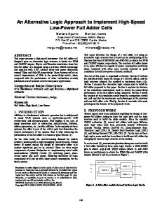
An Hybrid eDRAM/SRAM Macrocell to Implement First-Level Data Caches Alejandro Valero1 , Julio Sahuquillo1 , Salvador Petit1 , Vicente Lorente1 , Ramon Canal2 , Pedro López1 , José Duato1 1
2
Dpto. de Informática de Sistemas y Computadores Universidad Politécnica de Valencia, Valencia, Spain
[email protected] {jsahuqui, spetit, vlorente, plopez, jduato}@disca.upv.es
Department of Computer Architecture Universitat Politècnica de Catalunya, Barcelona, Spain
[email protected]
ABSTRACT
1.
SRAM and DRAM cells have been the predominant technologies used to implement memory cells in computer systems, each one having its advantages and shortcomings. SRAM cells are faster and require no refresh since reads are not destructive. In contrast, DRAM cells provide higher density and minimal leakage energy since there are no paths within the cell from Vdd to ground. Recently, DRAM cells have been embedded in logic-based technology, thus overcoming the speed limit of typical DRAM cells. In this paper we propose an n-bit macrocell that implements one static cell, and n-1 dynamic cells. This cell is aimed at being used in an n-way set-associative first-level data cache. Our study shows that in a four-way set-associative cache with this macrocell compared to an SRAM based with the same capacity, leakage is reduced by about 75% and area more than half with a minimal impact on performance. Architectural mechanisms have also been devised to avoid refresh logic. Experimental results show that no performance is lost when the retention time is larger than 50K processor cycles. In addition, the proposed delayed writeback policy that avoids refreshing performs a similar amount of writebacks than a conventional cache with the same organization, so no power wasting is incurred.
Static Random Access Memories (SRAM) and dynamic RAM (DRAM) have been the predominant technologies used to implement memory cells in computer systems. SRAM cells, typically implemented with six transistors (6T cells) have been usually designed for speed, while DRAM cells, implemented with only one capacitor and the corresponding pass transistor (1T1C cells) have been generally designed for density. Because of this reason, the former technology has been used to implement cache memories and the latter for main memory storage. Cache memories occupy an important percentage of the overall die area. A major drawback of these memories is the amount of dissipated static energy or leakage, which is proportional to the number of transistors used to implement these structures. Furthermore, this problem is expected to aggravate further provided that the transistor size will continue shrinking in future technologies. Many research work has tackled this problem in 6T SRAM cells [4, 7] by either reducing or removing the power supply to selected cache blocks. However, although leakage currents are reduced, they still persist. In contrast, dynamic 1T1C cells avoid this drawback by design, since the power supply is removed after accessing the memory cells. Typically, 1T1C DRAM cells were too slow to implement processor caches. However, technology advances have recently allowed to embed DRAM cells using CMOS technology [9]. An embedded DRAM cell (eDRAM) integrates a trench DRAM storage cell into a logic-circuit technology. In this way, the read operation delays can come out to have similar values than SRAM. As a consequence, recent commercial processors use eDRAM technology to implement L2 caches [13, 14]. Despite technology advances, an important drawback of DRAM cells is that reads are destructive, that is, the capacitor loses its state when it is read. In addition, capacitors lose their charge along time, thus they must be recharged or refreshed. To refresh memory cells, extra refresh logic is required which in turn results not only in additional power consumption but also in availability overhead. That is, when a block of a data array (i.e., a bank) is being refreshed no other line in the bank can be accessed. Due to these drawbacks, pure eDRAM cells do not seem appropriate to implement first-level data caches, where availability is a major design issue. Table 1 summarizes the main design characteristics of the discussed cells. In this paper we propose a macrocell which combines SRAM and eDRAM technologies aimed at being used at the first level
Categories and Subject Descriptors B.3.1 [Semiconductor Memories]: Dynamic memory (DRAM), Static memory (SRAM); B.3.2 [Design Styles]: Associative memories, Cache memories
Keywords Static and dynamic memory cells, retention time, leakage current
Permission to make digital or hard copies of all or part of this work for personal or classroom use is granted without fee provided that copies are not made or distributed for profit or commercial advantage and that copies bear this notice and the full citation on the first page. To copy otherwise, to republish, to post on servers or to redistribute to lists, requires prior specific permission and/or a fee. MICRO’09, December 12–16, 2009, New York, NY, USA. Copyright 2009 ACM 978-1-60558-798-1/09/12 ...$10.00.
INTRODUCTION
Technology
SRAM (6T)
DRAM (1T1C)
eDRAM
Access time
fast
slow
slow
Density
low
high
high
Leakage
high
low
low
Refresh
no
yes
yes
Destructive reads
no
yes
yes
Table 1: Memory cell characteristics data caches. The term macrocell refers to the proposed memory structure that consists of n memory cells, one SRAM cell and n-1 eDRAM cells, and pass transistors that communicate static to dynamic cells. In this way, by design, leakage and area are attacked due to the eDRAM cells, which in turn provides six to eight times as much memory as SRAM in the same area. The storage capacity of the macrocell defines the number of ways in the set-associative cache, that is, to implement a n-way set-associative cache a n-bit macrocell is required. Architectural innovations have been also devised to avoid refresh logic in the proposed macrocell, which is the major drawback of eDRAM cells. To this end, the cache controller is enhanced in two main ways: first, by moving the contents of dynamic cells to static cells when they are read, and then, by devising new writeback policies. Experimental results show that no performance is lost when not refreshing for DRAMs with a retention time larger than 50K processor cycles. In addition, the proposed delayed writeback policy performs a similar amount of writebacks with no refresh than a conventional cache with the same organization, so no power wasting is incurred. The remainder of this paper is organized as follows. Section 2 describes and analyzes the design of the proposed cell. Section 3 discusses the architectural innovations. Section 4 analyzes the experimental results. Section 5 summarizes the related research. Finally Section 6 presents some concluding remarks.
2.
MEMORY CELL PROPOSAL
Figure 1 shows the implementation of a 2-bit macrocell consisting of a typical 6T SRAM cell, 1-bit storage cell representing the eDRAM cell, and a bridge communicating both cells. The static part is limited to only one memory cell mainly due to leakage and area reasons. It has the same structure than a typical 6T static cell. Thus, read and write operations in this cell are managed in the same
Figure 1: Macrocell block diagram
a) Write 0 static to dynamic operation
b) Write 1 static to dynamic operation Figure 2: Static to dynamic write operation detail way as in a typical static cell through bit line (BLs) and its complementary (/BLs). The dynamic cell of the macrocell works as a typical 1T1C dynamic memory cell. The dynamic cell capacitor has a NMOS pass transistor (controlled by WL-d) that keeps the capacitor charge insulated from the bit line (BLd). Likewise the static part, read and write operations perform as in a conventional dynamic cell through the pass transistor. This design can be easily extended to an n-bit capacity storage by simply replicating the dynamic cell to store n-1 bit. Information movements among two different cells (e.g., static to dynamic) would imply two main steps in a conventional design: i) read the static content and write it to an intermediate buffer, and ii) read the buffer and write its content to the dynamic part. The main novelty of the design is the transistor that acts as a unidirectional bridge to move data from the static to the dynamic cell. The information state in the static cell can move directly to the capacitor, that is, with no need of intermediate buffers. These transferences will be referred to as internal since no bit line is involved. Notice that implementing a cache using macrocells instead of a split L1 cache (a standard SRAM and an eDRAM cache) has important advantages. First, some resources (decoder, wordline, etc.) can be shared. Second, when using two independent caches, the swap process (i.e., moving a block from static to dynamic and viceversa) involves much more circuitry and wire delays, prohibitively increasing latency and power dissipation.
a) Conventional cache
b) Macrocell-based cache Figure 3: Access and timing for conventional caches and macrocell-based caches In order to check the correctness of the electronic behavior, the proposed cell has been modeled in NGSPICE, a Berkeley’s Spice3f5 based circuit simulator. NGSPICE allows to accurately simulate MOSFET behavior since it uses BSIM4 MOSFET model. All the simulations are based on Predictive Technology Models (PTM) [18]. Values of key technology metrics of transistors have been taken from the 2007 ITRS [1] for 65nm technology nodes. Two main design issues were addressed to ensure the correct functionality of the proposed cell: i) to check that the capacitor is properly charged, and ii) the absence of flips when moving data from the static cell to the dynamic cell. Regarding the former issue, the main problem in a typical dynamic cell is the charge degradation when writing a ’1’ logic in the capacitor. This is due to NMOS pass transistors incur in a voltage drop equal to Vth when they transfer a ’1’ logic. Thus, in order to charge the capacitor to the maximum Vdd voltage, wordlines are usually boosted to a voltage, Vpp = Vdd + Vth. For eDRAM cells, Vth and Vdd are usually set to 0.44V and 1.2V respectively for 65nm technology nodes. Regarding the macrocell, the wordlines controlled by WL-d and S2D must be also boosted. Concerning the second design issue, read operations in conventional SRAM cells must be preceded by the precharge of both bitlines high. Precharge operations are necessary to optimize the cell speed, area, and stability relationship [16]. This is mainly due to the differences between NMOS and PMOS transistor features. In this way, flips are avoided inside the cell since NMOS transistors are stronger (i.e. can drive more current) than PMOS transistors. Analogously, to prevent flips in the proposed design, the capacitor
of the dynamic cell must be precharged to Vdd. Figure 2 illustrates how the internal write operation works (both writing a ’1’ and a ’0’). It highlights both the precharge process and how flips are avoided. It can be appreciated that the write access time is about 1ns (write 0). Besides correctness, as the capacitor is loosing charge along time, the retention time of the dynamic cell (i.e., the time that a DRAM cell can no longer hold the stored value) has been calculated using the CACTI5.3 model [15], assuming a 20fF capacitor included in typical implementations [16], which incurs a retention time by about 0.4 ms. The proposed macrocell reduces both leakage and area. Since leakage is mainly produced only by the SRAM cell, the macrocell will reduce leakage proportionally to the number of implemented dynamic cells. For instance, a 4-bit macrocell used in a four-way set-associative cache has 1 SRAM cell and 3 eDRAM cells. Ideally, as only the SRAM cell has leakage, the 4-bit macrocell achieves 75% (i.e., 3/4) less leakage than the same cache implemented with SRAM cells. Area is also reduced since the 4-bit macrocell requires half the transistors (i.e., 12=6+2x3) required by a four-way set-associative cache with 6T SRAM cell. Finally, notice that the higher the associativity degree supported by a macrocell, the larger the leakage saving and area reduction. As read operations in a dynamic cell are destructive and capacitors lose their charge along time, refresh actions are usually required. In this context, to avoid extra logic and power dissipation due to refresh operations, architectural innovations have been devised, explained below.
3.
ARCHITECTURAL DESIGN ISSUES
As mentioned above, the proposed n-bit macrocell has been designed with the aim of implementing the data array of a n-way setassociative cache, having one way implemented with static cells and n-1 ways with dynamic cells. From now on, we assume that the static cell implements the way-0 of the cache. The tag array of such caches is assumed to be implemented with typical 6T memory cells, thus the reading of any tag is not a destructive operation. The architectural scheme we devise to this cell consists of three main steps: i) accessing the dynamic cells only on a hit in the corresponding tag, ii) increasing the percentage of hits in the static blocks in order to minimize the number of data movements from dynamic to static, and iii) minimizing the number of writebacks to L2. Below, we detail these steps.
3.1
Accessing the Dynamic Cells
Typically, to achieve high performance, modern microprocessors overlap the access to the data and tag arrays. In this way, the requested data can be already available in case of a successful tag comparison (i.e., a cache hit). Figure 3(a) shows the accessed parts (dark boxes) in a four-way cache. The box in the left (the smallest one) represents the tag and the right box represents the data cache block. This working behavior is not adequate for data arrays implemented with macrocells; since regardless what the access results in (i.e. a cache hit or cache miss) reading the dynamic cells is destructive, and the design does not include refresh logic. Due to this reason, architectural solutions have been devised in order to avoid data cache blocks lose their contents. In order to guarantee correct execution, the problem is not that a given cache block loses its state along time but that it becomes unrecoverable. That is, the information loss is not a problem for correctness if it can be recovered from another location, for instance, from the L2 cache. The solution we devise to deal with this problem has two main
design goals: first, to reduce the number of state losses due to reads, and second, to provide a recoverable location without negatively impacting performance. To achieve the first design goal, the tags of all ways in the set are accessed in parallel (see the upper side of Figure 3(b)) at the same time as the data array of the block located in way-0 (static block). On a hit in way-0, the processor is satisfied and no dynamic cell is subsequently read. This access could obtain the hit speed of a direct-mapped cache since the multiplexer control signals could be set early, similarly as done in way-prediction techniques [3, 6]. On a miss in way-0 but a hit in other dynamic tag, the corresponding data array is accessed subsequently. To illustrate this case, the lower part of Figure 3(b) represents a hit in way-2. In this case, the data is read and provided to the processor. However, since this operation is destructive, the capacitor state is lost. A straightforward solution to address this drawback is to implement a write-through policy so that a copy of the data can be always read from the L2 if the capacitor is discharged. However, this way will yield to huge energy wasting in L2 caches as well as poor performance.
3.2
Out of order Hybrid gShare/bimodal: Gshare has 14-bit global history plus 16K 2-bit counters. Bimodal has 4K 2-bit counters, and choice predictor has 4K 2-bit counters Branch predictor penalty 10 cycles Fetch, issue, commit width 4 instructions/cycle ROB size (entries) 256 # Int. ALU’s 4 # FP ALU’s 4 Memory hierarchy Memory ports L1 data cache L1 data cache hit latency L2 data cache L2 data cache hit latency Memory access latency
Increasing the Percentage of Hits in the Static Cell
Some previous works [10] concluded that, because of data locality, in a two-way set-associative cache, most of the accesses hit the MRU (most recently used) block while few of them hit the LRU (least recently used) block, as shown in Figure 4. This conclusion can be generalized to caches with a higher number of ways as shown in Section 4. Based on this assert, a simple way to implement a way predictor is to predict the MRU line. The previous reason results in the modification of the cache controller in order to keep the MRU block always in the static cells of the macrocell. To this end, we enhance the cache controller in order to internally manage a swap among dynamic and static cells. The swap operation works as follows. Assume that the processor issues a load that hits a block stored in the dynamic cells. Then, the state of dynamic cells, which has been already read is written to an intermediate buffer. After that, the cache controller activates the S2D signal to move the contents of the static cell to the dynamic cell of the macrocell previously read. Finally, the data in the intermediate buffer is written to the static cells. If each of the previous steps consumes one cycle, then the controller will be busy for three processor cycles. However, the processor can get the requested data earlier from the intermediate buffer. Store instructions analogously perform in three steps. Notice that writes in the dynamic cells are always done as internal movements from the static cells, and they are not always trig-
MRU
1
L1 Hit Rate
Microprocessor core Issue policy Branch predictor type
No MRU 0.038 0.041
0.8 0.6
0.929 0.867
0.4
0
gzip vpr gcc mcf crafty parser eon perlbmk gap vortex bzip2 twolf wupwise swim mgrid applu mesa galgel art equake facerec lucas fma3d sixtrack apsi Int FP
0.2
Int
FP
Avg
Figure 4: L1 hit rate of the benchmarks in a 16KB-2way 64B/line cache.
4 Variable Split into hits in the dynamic and static parts 512KB, 8 ways, 64 byte-line 10 cycles 100 cycles
Table 2: Machine parameters gered by store instructions. Instead, they may be caused by a hit in the dynamic cells (load or store). To sum up, capacitors lose their charge along time, but those storing information in use will not need to be recharged since before losing their state this information will have been previously saved in the static cells. Finally, since we assume that the tag array is implemented with typical 6T memory cells, tags do not need to be swapped. Therefore, control information is needed to track the correspondence between tags and the corresponding data block. For a 2-way cache, the LRU bit is enough to link tags and data blocks. For a 4-way cache, 2-additional bits can be used.
3.3
Devised Writeback Policies
Although the architectural decisions discussed in the previous section avoid many capacitor state losses, they do not guarantee that cache blocks preserve their state when they are accessed. Thus, incorrect execution could occur when accessing a dirty block stored in dynamic cells. To deal with such situation, two new writeback policies have been devised. These policies will be referred to as early writeback and delayed writeback. The early writeback policy avoids the problem by preventing dirty blocks to be stored in dynamic cells. As a block can only be written into dynamic cells due to an internal swap operation, this policy checks the state of the block located in way-0 (static way) when a swap rises and, if dirty, the block is written back to L2. The main drawback of this policy is that it might increase the number of writes to L2 so turning on excessive energy wasting. This policy assumes that the valid bit of each dynamic way is implemented as a 1T-1C cell, including a capacitor with less capacitance than the macrocell capacitors that acts as a sentry bit. In this way, its charge indicates if the block is still preserving its contents or not. The delayed writeback policy is aimed at minimizing the number of writebacks to L2. To this end, this policy allows that dirty blocks can move to the dynamic cells. Once moved, capacitors maintain their state as dirty along the retention time. In this case, if the block is accessed again within the retention time, the block is forced to be rewritten to the static cells so preserving its state, otherwise,
Static Part
Dynamic Part
Static Part
0.929 0.867
0.4
0.8
0.896 0.818
0.4
0.2
0.2
0
0
FP
0.076 0.092
0.6
Avg
gzip vpr gcc mcf crafty parser eon perlbmk gap vortex bzip2 twolf wupwise swim mgrid applu mesa galgel art equake facerec lucas fma3d sixtrack apsi Int FP
0.6
L1 Hit Rate
0.038 0.041
0.8
Int
Int
a) 16KB-2way
Static Part
FP
Avg
b) 16KB-4way
Dynamic Part
Static Part
Dynamic Part
1
0.8 0.6
0.953 0.899
0.4
0.6
0
gzip vpr gcc mcf crafty parser eon perlbmk gap vortex bzip2 twolf wupwise swim mgrid applu mesa galgel art equake facerec lucas fma3d sixtrack apsi Int FP
0.2
0
FP
Avg
0.929 0.867
0.4
0.2
Int
0.049 0.07
0.8
gzip vpr gcc mcf crafty parser eon perlbmk gap vortex bzip2 twolf wupwise swim mgrid applu mesa galgel art equake facerec lucas fma3d sixtrack apsi Int FP
0.023 0.033
L1 Hit Rate
1
L1 Hit Rate
Dynamic Part
1
gzip vpr gcc mcf crafty parser eon perlbmk gap vortex bzip2 twolf wupwise swim mgrid applu mesa galgel art equake facerec lucas fma3d sixtrack apsi Int FP
L1 Hit Rate
1
Int
c) 32KB-2way
FP
Avg
d) 32KB-4way
Figure 5: L1 hit rate for different cache organizations the state would be lost. To avoid the latter case, the solution we propose is to access each block periodically before the retention time expires, and if it is dirty, the block is written back to L2 instead of L1 (which keeps the MRU block). This idea can be implemented with a single global binary counter [7, 8] for all dynamic blocks. The counter is decremented every cycle, and each time that the counter reaches zero, a given dynamic block accessed following a given criterion (e.g., circular order) is checked to be written back. The counter must be initialized to the retention time divided by the number of dynamic blocks. In this policy, the valid bit can can be implemented in two different ways, i) by using a sentry bit similarly as done in the previous policy, and ii) by clearing the valid bit each time the block is checked wether or not it is written back to L2. Since both of them provide similar performance, the first one was assumed across the experiments due to homogeneity reasons.
4.
EXPERIMENTAL EVALUATION
This section presents the simulation environment and the benchmarks used to evaluate performance and energy consumption in microprocessors implementing caches with macrocells. These cells have been modeled on top of an extensively modified version of the hotleakage simulation framework [17]. Table 2 summarizes the architectural parameters used through the experiments. The delayed writeback policy has been used by default. Experimental results were obtained configuring the hotleakage framework for the Alpha ISA and running the SPEC2000 benchmark suite [2]. Both integer (SpecInt) and floating-point (SpecFP) benchmarks have been evaluated using the ref input sets, where we skip for all benchmarks 1000M instructions before collecting statistics, and then simulate 500M instructions.
4.1
Static and Dynamic Hit Rate
A read in the dynamic cells requires from a refresh operation since reads are destructive, even if the access results in a cache miss. Hence, to avoid unnecessary refresh operations, dynamic cells are only accessed on cache hits. This section characterizes such accesses. We use the term static hit rate to refer to the percentage of cache accesses that hit on the static cache way, and the term dynamic hit rate to refer to the percentage of accesses that hit a dynamic way. The sum of both will give the L1 hit rate. Figure 5 shows the results for different cache sizes (16KB and 32KB) and number of ways (2 and 4). As a n-bit macrocell has only one static cell, the storage capacity of the static cells is the cache size divided by the number of bits of the macrocell, that is, divided by the number of cache ways. For instance, the static storage capacity of a 16KB-2way and a 32KB4way cache is 8KB. An important observation is that due to the architectural mechanism that enforces the storage of the MRU block in the static cache way (way-0), the number of hits in way-0 only depends on its storage capacity. For instance, the hit rate of the static part of a 16KB2way matches the one of a 32KB-4way and both caches have a 8KB static data array. Hence, both arrays will produce the same amount of misses, the difference is that the incoming block may be fetched from different memory structures (e.g., dynamic cells or other level of the memory hierarchy). Notice that for a given cache size, the higher the associativity degree the smaller the size of the static way. Hence, although increasing the number of ways yields to a higher overall L1 hit rate, the static hit rate decreases with the number of ways and the dynamic hit rate increases.
99.92
99.56
99.92
99.34
99.68
98 97.31 96 94 92
Normalized Performance (%)
Normalized Performance (%)
100
100 99.88
99.34
99.68
(1,2)
2-cycle
99.88
99.72
(1,2)
2-cycle
97.32
96 94 92 90
90 1-cycle
(1,1)
(1,2)
2-cycle 1-cycle
(1,1)
Int
(1,2)
1-cycle
2-cycle
(1,1)
(1,2)
FP
99.88
99.68
98 97.27
96 94 92
Normalized Performance (%)
99.88
99.56
(1,1) FP
b) 16KB-4way
100 99.73
2-cycle 1-cycle
Int
a) 16KB-2way
Normalized Performance (%)
99.84
98.85
98
90
100 99.92
99.56
99.29
98
97.27
96 94 92 90
1-cycle
(1,1)
(1,2)
2-cycle 1-cycle
Int
(1,1)
(1,2)
2-cycle
1-cycle
(1,1)
FP
(1,2)
2-cycle 1-cycle
Int
c) 32KB-2way
(1,1) FP
d) 32KB-4way Figure 6: Normalized performance (IPC)
Results show the effectiveness of the devised architectural mechanism since the dynamic hit rate is, on average, less than 4.1% for 2-way caches regardless the benchmark type (integer or floatingpoint) and cache size. This value grows up to 9.2% for SpecFP benchmarks in the 16KB 4-way cache configuration, but in this case, the overall L1 hit rate is also larger. Notice that this value is interesting to be small due to two main reasons: first, the overall access time of the dynamic cells requires an additional processor cycle for tag comparison, and second, a hit in a dynamic way incurs a swap between a dynamic and the static way.
respectively. Remember that a hit in a dynamic way would require an additional processor cycle to check the tags. As observed, the proposed macrocell induces almost no adverse impact on performance, since performance degradation is always less than 1%. The only exception rises for integer benchmarks in the 16KB-4way cache. In contrast, the performance of the twocycle conventional cache drops down to about 3%. Regarding floating-point benchmarks minor performance differences appear neither due to the slower two-cycle conventional cache in the modeled machine nor in the proposed macrocell.
4.2
4.3
Impact of Dynamic Access Time on Performance
Results provided by CACTI 5.3 [15] indicate that an eDRAM cell can be accessed as fast as an SRAM, as also stated in [9], although writes can be slightly slower. This section evaluates the impact on performance of the macrocell varying the access time of the dynamic ways (1 and 2 cycles), while keeping constant (1 cycle) the access time of the static way. Notice that a fast conventional cache with just one-cycle access time imposes an upper-bound in performance (i.e., IPC) to the proposal since there is no performance loss. Figure 6 shows the normalized performance with respect to the conventional cache with the same organization. For comparison purposes, the values of a two-cycle access time conventional cache are also plotted. The X axis presents the access times of the different cache organizations. Conventional caches are labeled as 1cycle and 2-cycle. Access times of the macrocell based caches are labeled as pairs (1,x), where the first and second elements refer to the access time of the static and dynamic cells in processor cycles,
Impact of Retention Time on Performance
In the previous section we evaluate the performance degradation of the macrocell with respect to a conventional SRAM. In that study we assumed a perfect capacitor with no charge looses. Nevertheless, real capacitors lose their state after a given retention time. Therefore, accessing the dynamic cells after this time requires the access to a lower level of the memory hierarchy to get the requested data, thus, adversary impacting the performance. This section explores the impact of retention time on performance with respect to a perfect capacitor. Figure 7 shows the results ranging the retention time from 100 to 50K processor cycles. As observed, for each cache organization, retention times longer than 50K cycles do not provide any hit rate improvements; thus, no performance degradation can be observed. Moreover, in the 16KB-2way cache, just 10K cycles are enough to match the hit rate of a perfect capacitor. For a given associativity degree, the larger the cache size (i.e., 32KB) the lower the performance losses (due to the larger static part of the cache). In contrast, for given cache size, the higher
3.5
Performance Degradation (%)
Int
FP
3 2.5 2 1.5 1 0.5
Performance Degradation (%)
3.5
0
Int 2.5 2 1.5 1 0.5 0
100
500
1000 5000 Retention Time (cycles)
10000
50000
100
500
a) 16KB-2way
1000 5000 Retention Time (cycles)
10000
50000
b) 16KB-4way
3.5 Int
FP
3 2.5 2 1.5 1 0.5
Performance Degradation (%)
3.5
Performance Degradation (%)
FP
3
Int
FP
3 2.5 2 1.5 1 0.5 0
0 100
500
1000 5000 Retention Time (cycles)
10000
100
50000
500
c) 32KB-2way
1000 5000 Retention Time (cycles)
10000
50000
d) 32KB-4way Figure 7: IPC losses varying the retention time
4.4
0.04 Replacement
Swap
Sporadic
WB Rate
0.03
0.02
0.01
Conv Early Delayed Conv Early Delayed Conv Early Delayed Conv Early Delayed Conv Early Delayed Conv Early Delayed Conv Early Delayed Conv Early Delayed
0
16KB2way
16KB4way
32KB2way Int
32KB4way
16KB2way
16KB4way
32KB2way
32KB4way
FP
Figure 8: Writeback rate for the devised policies and the conventional cache the associativity degree the larger the performance losses (due to the larger number of hits in the dynamic part -i.e. larger dynamic part). Finally, larger dynamic parts require longer retention times to stabilize performance To sum up, the proposal just requires from capacitors which retain their charge for a few thousands of processor cycles in order to achieve its maximum performance. That means, that the DRAM capacitor charge can be several orders of magnitude lower than the studied in Section 2, which will be enough to avoid performance losses due to the retention time.
Writeback Policies Evaluation
A writeback to L2 in a conventional writeback cache rises when a dirty block is evicted from L1. In addition to writebacks due to replacements, new types of writebacks can be identified in the devised policies. Regarding the early writeback policy, two types of writebacks can be distinguished. First, the static block must move to a dynamic way in order to make room to the missing block. In such case, if the static block is dirty it must be written back to L2. In addition, a writeback can be also performed due to a swap risen as consequence of a dynamic hit. Thus, there are writebacks due to replacements and due to internal swaps. Regarding the delayed policy, writebacks due to replacements only can occur in the dynamic ways. In addition, writebacks can also rise driven by the interval counter, this kind of writebacks will be referred to as sporadic writebacks. To evaluate the effectiveness of the devised policies we obtained the corresponding writeback rate for each writeback class appearing in such policy, calculated as the number of blocks written back divided by the number of accesses to L1. Figure 8 shows the cumulative results for a 50K-cycle retention time. As observed, for a given cache organization and benchmark type, the replacement writeback rate is quite uniform across the studied policies. Regarding the early policy, its swap writeback rate leads to an important amount of blocks written back to L2. Comparing this rate to the sporadic rate of the delayed policy, we can state that the early policy is too conservative since many blocks are written back unnecessarily so incurring power wasting. In short, the proposed delayed writeback policy performs a similar amount of writebacks with no refresh than a conventional cache with the same organization, so no power wasting is incurred.
4.5
Estimating Energy Savings
Although the main objective of this paper is to demonstrate the suitability of combining SRAM and DRAM cells in an L1 cache in terms of feasibility and performance, as well as proposing architectural solutions to deal with such a cell; it is also important to quantify the effect on power of such alternative. Regarding energy, a 4-bit macrocell roughly reduces the leakage current about 75% with respect to a 4-way conventional cache since the four original SRAM cells turn into 1 SRAM and 3 DRAM cells. As DRAM cells have minimal leakage current since there are no paths within the cell from Vdd to ground; one can extrapolate that leakage will be reduced from the achieved by 4 SRAMs to the one of 1 SRAM (i.e. 75%). In contrast, dynamic energy has a new component not present in conventional caches; that is, the due to swaps or internal movements (i.e., from static to dynamic). As mentioned above, a swap occurs due to dynamic hits. In addition, movements from static to dynamic can also rise as consequence of L1 misses. To quantify this energy overhead lets consider the worst case (i.e., the 16KB-4way cache organization). As shown in Figure 5, this organization has both the larger dynamic hit rate and miss rate. The sum of both rates represents, on average, about 10% and 18% of the whole cache accesses for the SpecInt and SpecFP benchmarks, respectively. Thus, these numbers would represent approximately the estimated overhead (i.e. extra activity). In summary, in a 16KB-4way cache the proposed macrocell reduces leakage current about 75% while it increases -in the worst case- the dynamic energy about 10% and 18% depending on the workload. Taken into account that in a 65nm technology the static energy represents around 38% the whole energy [11], we can state that the proposal guarantees a energy savings about 22% (75×0.38– 10×0.62) and 17% with respect to the total energy dissipated by the L1 data cache, for integer and floating-point benchmarks, respectively. Moreover, these benefits are expected to be larger in future technologies since static energy weight grows as the transistor size shrinks. For instance, in a 45nm technology, where leakage represents about 48%, the total energy savings grows up to 31%, and 27%.
5.
RELATED WORK
Reducing leakage has been widely studied in recent years in conventional SRAM caches. The proposed techniques can be classified in two main groups depending on whether the block state is preserved or not. In the first group, the voltage supply to selected cache lines is reduced and the lines are put in a low-power drowsy mode, so increasing the access time to such lines [4, 10]. In the second group, the voltage supply to the cache blocks with poorer locality is removed, thus, losing the block information [7, 12]. Subsequent accesses to such blocks will result on a cache miss, thus, the next level of the memory hierarchy must be accessed. Implementation of embedded DRAM 1T1C cells has been made in two main ways: DRAM-based and logic-based implementation. Initially, the consensus was that the use of DRAM-based eDRAM was the correct strategy for system evolution, because of its cheaper processing although its slower access time. In contrast, logic-based eDRAM produces fast devices but it requires adding the DRAM deep trench and other processes to the logic process which was seemingly more difficult and expensive. Matick and Schuster [9], from the IBM technology group, thought that the use of logic-based eDRAM to embed 1T1C cells would be the most feasible way to reduce the increasing gap in speed, measured in processor cycles, between logic and DRAM memory technologies. Posterior work by the same Technology group led to the
inclusion of logic-based eDRAM in the IBM ASICs (applicationspecific integrated circuits) product. As a consequence several recent microprocessors implement L2 caches in this technology [13, 14]. Other research works have concentrated on the design on new DRAM cells to reduce leakage dissipation. Most of these cells could be fabricated using logic-based technology. In this context, Liang et. al [8] proposed the 3T1D DRAM cell for L1 data caches. This cell consists of three transistors and a diode with the aim to reduce the current leakage. This cell can be quickly accessed; however, the diode charge get lost over the passing time. Thus, refreshing actions are required. Juang et al. [5] proposed a dynamic cell based on static 6T cell but only with 4 transistors, resulting in a non-static cell (the quasi-static 4T cell). The 4T cells offer an easy method for DRAM implementation in a logic process production, especially in embedded systems. 4T cells mainly differ from the 6T SRAM cells in that they do not include the two transistors connected to Vdd that restore the charge loss due to the current leakage. Using the same transistor type, the 4T cell requires less area than the 6T SRAM cell while achieving almost the same performance. As opposite, the data access is a bit slower and destructive. As the 1T1C cell, this problem could solved re-writing the read data immediately after the read operation.
6.
CONCLUSIONS
Memory cells design for cache memories is a major concern in current microprocessors mainly due to the involved leakage, area, and access time. In this paper we have introduced the memory macrocell with a nbit capacity storage, and we have shown that combining SRAM and eDRAM technologies to implement a macrocell is feasible. An nbit macrocell can be straightforwardly used to implement first-level n-way set-associative caches with minimal impact on performance, since it addresses by design speed, area, and leakage consumption. Experimental results showed that compared to a conventional cache with the same capacity, i) leakage consumption remains only about one divided the number of the cache ways, ii) area can be largely reduced (e.g. as much as half in a 4-way set-associative cache), and it can be further reduced for a higher associativity degree, and iii) a relatively low capacitor charge is enough to avoid performance losses due to the retention time. Finally, remark that the devised delayed writeback policy allows to avoid the refresh logic, required in typical DRAM memory cells, with minimal impact on performance and power.
7.
ACKNOWLEDGMENTS
This work was supported by Spanish CICYT under Grant TIN 2006-15516-C04-01, by Consolider-Ingenio 2010 under Grant CSD 2006-00046, by Explora-Ingenio under Grant TIN2008-05338-E, and by Generalitat Valenciana under Grant GV/2009/043. Ramon Canal is supported by the Generalitat de Catalunya under Grant 2009SGR1250, and the Spanish Ministry of Science and Innovation under Grant TIN2007-61763.
8.
REFERENCES
[1] Semiconductor Industries Association, " International Technology Roadmap for Semiconductors", 2007, available online at http://www.itrs.net/. [2] Standard Performance Evaluation Corporation, available online at http://www.spec.org/cpu2000. [3] B. Calder, D. Grunwald, and J. Emer. Predictive Sequential Associative Cache. Proceedings of the 2nd International
[4]
[5]
[6]
[7]
[8]
[9]
[10]
[11] [12]
[13]
[14]
[15]
[16]
[17]
[18]
Symposium on High-Performance Computer Architecture, pages 244–253, 1996. K. Flautner, N. S. Kim, S. Martin, D. Blaauw, and T. Mudge. Drowsy Caches: Simple Techniques for Reducing Leakage Power. Proceedings of the 29th Annual International Symposium on Computer Architecture, pages 148–157, 2002. Z. Hu, P. Juang, P. Diodato, S. Kaxiras, K. Skadron, M. Martonosi, and D. W. Clark. Managing Leakage for Transient Data: Decay and Quasi-Static 4T Memory Cells. Proceedings of the 2002 International Symposium on Low Power Electronics and Design, pages 52–55, 2002. K. Inoue, T. Ishihara, and K. Murakami. Way-Predicting Set-Associative Cache for High Performance and Low Energy Consumption. Proceedings of the 1999 International Symposium on Low Power Electronics and Design, pages 273–275, 1999. S. Kaxiras, Z. Hu, and M. Martonosi. Cache Decay: Exploiting Generational Behavior to Reduce Cache Leakage Power. Proceedings of the 28th Annual International Symposium on Computer Architecture, pages 240–251, 2001. X. Liang, R. Canal, G.-Y. Wei, and D. Brooks. Process Variation Tolerant 3T1D-Based Cache Architectures. Proceedings of the 40th Annual IEEE/ACM International Symposium on Microarchitecture, pages 15–26, 2007. R. E. Matick and S. E. Schuster. Logic-based eDRAM: Origins and rationale for use. IBM Journal of Research and Development, 49(1):145–165, 2005. S. Petit, J. Sahuquillo, J. M. Such, and D. Kaeli. Exploiting Temporal Locality in Drowsy Cache Policies. Proceedings of the 2nd conference on Computing frontiers, pages 371–377, 2005. S. Piccioni. Real Design Challenges of Low Power Physical Design Implementation. Sylicon and Sofware Systems, 2007. M. Powell, S.-H. Yang, B. Falsafi, K. Roy, and T. N. Vijaykumar. Gated-Vdd: A Circuit Technique to Reduce leakage in Deep-Submicron Cache Memories. Proceedings of the 2000 International Symposium on Low Power Electronics and Design, pages 90–95, 2000. B. Sinharoy, R. N. Kalla, J. M. Tendler, R. J. Eickemeyer, and J. B. Joyner. POWER5 System Microarchitecture. IBM Journal of Research and Development, 49(4/5):505–521, 2005. J. M. Tendler, J. S. Dodson, J. S. Fields, H. Le, and B. Sinharoy. POWER4 System Microarchitecture. IBM Journal of Research and Development, 46(1):5–25, 2002. S. Thoziyoor, N. Muralimanohar, J. H. Ahn, and N. P. Jouppi. CACTI 5.1. Hewlett-Packard Laboratories, Palo Alto, Technical Report, 2008. N. H. E. Weste, D. Harris, and A. Banerjee. CMOS VLSI Design: A Circuits and Systems Perspective. Pearson/Addison-Wesley, 2005. Y. Zhang, D. Parikh, K. Sankaranarayanan, K. Skadron, and M. Stan. Hotleakage: A Temperature-Aware Model of Subthreshold and Gate Leakage for Architects. University of Virginia Department of Computer Science, Technical Report, 2003. W. Zhao and Y. Cao. Predictive Technology Model for Nano-CMOS Design Exploration. Journal on Emerging Technologies in Computing Systems, 3(1):1–17, 2007.