Implementation of new technology (power electronics) in the field of agriculture. ...... $4.14. Digikey. FAN7393AMXCT-ND. Available. Boot diodes. Vish ay 1. N4.
Design and Implementation of an off-grid PV drive system for small-scale fresh produce cooling by
Jason Avron Samuels
Thesis presented in partial fulfilment of the requirements for the degree of Master of Engineering (Electrical and Electronic) in the Faculty of Engineering at Stellenbosch University
Department of Electrical and Electronic Engineering, University of Stellenbosch, Private Bag X1, Matieland 7602, South Africa.
Supervisor: Dr. J. M. Strauss
December 2017
Stellenbosch University https://scholar.sun.ac.za
Declaration By submitting this thesis electronically, I declare that the entirety of the work contained therein is my own, original work, that I am the sole author thereof (save to the extent explicitly otherwise stated), that reproduction and publication thereof by Stellenbosch University will not infringe any third party rights and that I have not previously in its entirety or in part submitted it for obtaining any qualification.
Date:
December 2017
Copyright © 2017 Stellenbosch University All rights reserved.
i
Stellenbosch University https://scholar.sun.ac.za
Abstract Design and Implementation of an off-grid PV drive system for small-scale fresh produce cooling J. Samuels Department of Electrical and Electronic Engineering, University of Stellenbosch, Private Bag X1, Matieland 7602, South Africa.
Thesis: M.Eng (E & E) December 2017 The implementation of a PV drive system is discussed in this thesis with the focus on fresh produce cooling for small-scale farmer. A background study is presented, which firstly addresses hunger and food insecurity through emphasis on one of the mentioned six causes of hunger, namely, food waste. Further focus is placed on cooling and, specifically, solar cooling. Therefore, the relevant factors pertaining to cooling and solar energy as a power source are presented, adding to the background study. Thereafter, the project details are outlined which states the research significance as the investigation of feasibility, in terms of cost and performance, of the design and implementation of PV drive systems, using the proposed development process. With that being said, the design of the PV drive system, elevation of low-voltage solar PV energy and cost-effective implementation were evaluated. In a high-level project overview the project parts are presented for the designed and implemented PV drive system, with the focus on the solar energy source and the cooling application. Similarly, the proposed development process is discussed through which the drive system was implemented. In effect, this process entails using off-the-shelf subsystems, as far as possible, to construct the drive system with only the necessary self-built subsystems. The drive system consists of the following self-built subsystems, namely the DC-DC converter and control module, and a commercial VSD, with integration between these subsystems. As the main means of voltage elevation, from the low-voltage solar PV source, the focus is placed on DC-DC converters. Furthermore, a comparison of DC-DC converters are made, with the defined criteria for the project, for the most suitable converter. For easier comparison, the converters are grouped and their advantages and disadvantages are presented. Ultimately, a converter choice was made. The chosen converter, the resonant push-pull converter, was thoroughly discussed, analysed and specifically designed for the project. Furthermore, this theoretical design of the converter was firstly simulated, for confirmation, before physical construction proceeded. Thereafter, converter tests were done to verify the design through various measurements. Most importantly, the converter output voltage range and efficiency were measured and verified to a satisfactory degree. ii
Stellenbosch University https://scholar.sun.ac.za
ABSTRACT
iii
The system control module allowed for proper operation of the converter and, moreover, the integration of the PV drive subsystems. Furthermore, the microcontroller-based control module is discussed and the implemented algorithms are presented for optimal energy transfer; these algorithms were expressed in flow diagrams. In addition, transient control results are shown for start-up and load variations for verification. After verification of the main subsystems, the complete PV drive system was operated throughout a whole day with an appropriate load, to ensure proper conclusions are made. Unfortunately, a cooling system could not be acquired for testing. Details for the demonstration are presented, which include the specific equipment used and results for the operation. Moreover, the results present a fully operational drive system from a lowvoltage solar PV energy source able to drive the appropriate load, which demonstrates successful performance. However, the drive system included performance shortfalls, which are discussed and for which recommendations were provided. With the drive system operational, conclusions were made, regarding cost and performance, in comparison with other similar systems. In addition, the research objectives and aims were evaluated. After evaluation, although the PV drive system could be designed and implemented to a successful measure with regards to performance, it fell short regarding cost in comparison with the compared systems. Therefore, the proposed PV drive system, with the development process followed, is not completely feasible in implementation -to the degree described- for fresh produce cooling for small-scale farmers.
Stellenbosch University https://scholar.sun.ac.za
Uittreksel Ontwerp en toepassing van ’n nie netwerkgeskakelde FV aandryfstelsel vir kleinskaalboerdery vars oes en opbrengs verkoeling J. Samuels Departement Elektriese en Elektroniese Ingenieurswese, Universiteit van Stellenbosch, Privaatsak X1, Matieland 7602, Suid Afrika.
Tesis: M.Ing (E & E) Desember 2017 Die implementering van ’n fotovoltaïese (FV) aandryfstelsel word bespreek in die tesis met die fokus op die verkoeling van vars produkte in kleinskaalboerdery. ’n Agtergrondstudie is aangebied wat eerstens hongersnood en voedselonsekerheid aanspreek met die klem op een van die ses genoemde oorsake van hongersnood, naamlik, voedselvermorsing. Verdere fokus is geplaas op verkoeling, spesifiek sonverkoeling, en die relevante faktore van verkoeling en sonenergie as bron is aangebied, in byvoeging tot die agtergrondstudie. Daarna is die projek besonderhede getoon wat die navorsingsbelang verklaar as die uitvoerbaarheidsondersoek, in terme van koste en uitvoering, van die ontwerp en toepassing van FV aandryfstelsels, met die voorgestelde ontwikkelingsproses. Met dit gesê, is die ontwerp van die FV aandryfstelsel, die verhoging van die laespanning FV sonenergie bron en koste-effektiewe toepassing geëvalueer. In ’n hoëvlak projekoorsig is die projekdele aangebied vir die ontwerp en toepassing van die FV aandryfstelsel met die fokus op die sonenergie as bron en die voerkoelingstoepassing. Soortgelyk is die voorgestelde ontwikkelingsproses bespreek waardeur die FV aandryfstelsel toegepas is. In effek bevat die proses die gebruik van van-die-rak substelsels, so ver mootlik, om die FV aandryfstelsel saam te stel met net die nodige selfgeboude substelsels. Die aandryfstelsel bestaan uit die volgende selfgeboude substelsels, naamlik, die g.s.-g.s. omsetter en die beheermodule, en ’n kommersieële veranderbare spoed aandrywer (VSA), met integrasie tussen die substelsels. As hoof manier van spanningsverhoging, vanaf die laespanning FV sonenergiebron, is die fokus geplaas op die GS-GS omsetter. Nog meer is ’n vergelyking van g.s.-g.s. omsetters gemaak, met die gekose kriteria vir die projek, vir die mees gepaste omsetter. Om die vergelyking makliker te maak is die omsetters gegroepeer en hulle voordele en nadele getoon. Uiteindelik is ’n omsetterkeuse gemaak. Die gekose omsetter, die resonante stoot-trek omsetter, is deuglik bespreek, geanaliseer en ontwerp spesifiek vir die projek. Nog meer, is die teoretiese ontwerp van die omsetter gesimuleer, vir bevestiging, voordat die fisiese samestelling voortgegaan is. Daarna is omsettertoetse gedoen om die ontwerp te bevestig deur verskeie metings. Mees belanglik iv
Stellenbosch University https://scholar.sun.ac.za
UITTREKSEL
v
is voldoende bevestiging van die omsetter se uittreespanningsbereikmetings en doeltreffendheidmetings. Die stelselbeheermodule het toegelaat vir behoorlike werking van die omsetter en, nogmeer, die integrasie van die FV aandryfstelseldele. Boonop is die mikrobeheerdergebaseerde beheermodule bespreek en die toegepaste algoritmes aangebied vir optimale energieoordrag; hierdie algoritmes is deur vloeidiagramme uitgedruk. Verder is die oordragsbeheerresultate getoon, van die omsetteraanskakeling en lasvariasies, vir bevesting. Na bevestiging van die hoofsubstelsels is die volledige FV aandryfstelsel bedryf vir ’n volle dag met ’n toepaslike las om te verseker dat gepaste gevolgtrekkings gemaak is. Ongelukkig is ’n verkoelingsstelstel nie verkry vir toetse nie. Besonderhere vir die demonstrasie is aangebied wat die informasie oor die spesifiek toerusting en resultate van die volle dag se bedryf insluit. Nog meer is die resultate aangebied van ’n werkende aandryfstelsel van ’n laespanning FV sonenergiebron om ’n toepaslike las aan te dryf, wat suksesvolle uitvoering demonstreer. Alhoewel die FV aandryfstelsel suksesvolle werking toon, is tekortkominge in werksverrigting waargeneem en bespreek met die nodige aanbevelings. Met die FV aandryfstelsel operasioneel, is gevolgtrekkings gemaak met betrekking tot koste en uitvoering saam, in vergelyking met ander soortgelyke stelsels. Nog meer is die navorsingsuitsette en navorsingsdoelwitte geëvalueer. Na die evaluering, alhoewel die FV aandryfstelselontwerp en toepassing tot suksesvolle uitvoeringsmate getoon is, val dit kort in terme van koste in vergelyking met soortgelyke stelsels. Dus is die voorgestelde FV aandryfstelsel met die ontwikkelingsproses gevolg, nie volledig uitvoerbaar in toepassing -tot die mate beskryf- vir vars produk verkoeling by kleinskaalboerdery nie.
Stellenbosch University https://scholar.sun.ac.za
Acknowledgments I would like to express my sincere gratitude and appreciation to the following people and organisations: • Dr. Strauss for his wisdom, guidance, support and patience throughout the thesis duration. His passion and attitude was truely a driving force of inspiration for myself; • My family and friends for their support and assistance; • The financial assistance of the National Research Foundation (NRF) towards this research is hereby acknowledged. Opinions expressed and conclusions arrived at, are those of the author and are not necessarily to be attributed to the NRF; • The university E & E workshop staff; and • finally, our heavenly Father.
vi
Stellenbosch University https://scholar.sun.ac.za
Contents Declaration
i
Abstract
ii
Uittreksel
iv
Contents
vii
List of Figures
xi
List of Tables
xvi
1 Introduction 1.1 Hunger and food insecurity . . 1.2 Food waste . . . . . . . . . . 1.3 Cooling . . . . . . . . . . . . 1.3.1 Food refrigeration . . . 1.3.2 Solar-cooling . . . . . 1.3.3 Compressors . . . . . . 1.4 Solar PV as an Energy source 1.5 Introduction to the project . . 1.6 Research question . . . . . . . 1.7 Problem statement . . . . . . 1.8 Research aims . . . . . . . . . 1.9 Research objectives . . . . . . 1.10 Significance of the Research . 1.11 Scope of the Research . . . . . 1.12 Proposed execution project . . 1.13 Thesis outline . . . . . . . . .
. . . . . . . . . . . . . . . .
. . . . . . . . . . . . . . . .
2 High-level project overview 2.1 Introduction . . . . . . . . . . . . 2.2 Development process . . . . . . . 2.3 Input source for the project . . . 2.3.1 Introduction . . . . . . . . 2.3.2 Resources for electricity . 2.3.3 Solar PV . . . . . . . . . . 2.3.4 Input source specifications 2.3.5 Cost of modules . . . . . . 2.3.6 Safety . . . . . . . . . . .
. . . . . . . . . . . . . . . . . . . . . . . . .
. . . . . . . . . . . . . . . . . . . . . . . . .
vii
. . . . . . . . . . . . . . . . . . . . . . . . .
. . . . . . . . . . . . . . . . . . . . . . . . .
. . . . . . . . . . . . . . . . . . . . . . . . .
. . . . . . . . . . . . . . . . . . . . . . . . .
. . . . . . . . . . . . . . . . . . . . . . . . .
. . . . . . . . . . . . . . . . . . . . . . . . .
. . . . . . . . . . . . . . . . . . . . . . . . .
. . . . . . . . . . . . . . . . . . . . . . . . .
. . . . . . . . . . . . . . . . . . . . . . . . .
. . . . . . . . . . . . . . . . . . . . . . . . .
. . . . . . . . . . . . . . . . . . . . . . . . .
. . . . . . . . . . . . . . . . . . . . . . . . .
. . . . . . . . . . . . . . . . . . . . . . . . .
. . . . . . . . . . . . . . . . . . . . . . . . .
. . . . . . . . . . . . . . . . . . . . . . . . .
. . . . . . . . . . . . . . . . . . . . . . . . .
. . . . . . . . . . . . . . . . . . . . . . . . .
. . . . . . . . . . . . . . . . . . . . . . . . .
. . . . . . . . . . . . . . . . . . . . . . . . .
. . . . . . . . . . . . . . . . . . . . . . . . .
. . . . . . . . . . . . . . . .
1 1 3 3 3 3 4 5 8 9 9 9 10 10 11 11 12
. . . . . . . . .
13 13 14 14 14 15 15 15 16 16
Stellenbosch University https://scholar.sun.ac.za
viii
CONTENTS
2.4
2.5 2.6 2.7
Drive system . . . . . . . . 2.4.1 Introduction . . . . . 2.4.2 Voltage Elevation . . 2.4.3 Control module . . . 2.4.4 Variable speed drive Cooling application . . . . . 2.5.1 Small scale farming . 2.5.2 Refrigeration . . . . Project specifications . . . . Research project execution .
. . . . . . . . . .
. . . . . . . . . .
. . . . . . . . . .
. . . . . . . . . .
. . . . . . . . . .
. . . . . . . . . .
. . . . . . . . . .
. . . . . . . . . .
. . . . . . . . . .
. . . . . . . . . .
. . . . . . . . . .
. . . . . . . . . .
. . . . . . . . . .
. . . . . . . . . .
. . . . . . . . . .
. . . . . . . . . .
. . . . . . . . . .
. . . . . . . . . .
. . . . . . . . . .
. . . . . . . . . .
. . . . . . . . . .
. . . . . . . . . .
. . . . . . . . . .
. . . . . . . . . .
3 DC-DC converter 3.1 Introduction . . . . . . . . . . . . . . . . . . . . . . . . . . . . . . . . . 3.2 DC-DC converters: A brief overview . . . . . . . . . . . . . . . . . . . 3.2.1 Introduction . . . . . . . . . . . . . . . . . . . . . . . . . . . . . 3.2.2 Elevation factors . . . . . . . . . . . . . . . . . . . . . . . . . . 3.2.3 From linear to switching power supplies . . . . . . . . . . . . . . 3.3 Resonant converter: a brief overview . . . . . . . . . . . . . . . . . . . 3.4 Criteria of the DC-DC converter choice . . . . . . . . . . . . . . . . . . 3.5 Non-isolated converter group . . . . . . . . . . . . . . . . . . . . . . . . 3.5.1 Boost converter . . . . . . . . . . . . . . . . . . . . . . . . . . . 3.5.2 Interleaved Boost Converter . . . . . . . . . . . . . . . . . . . . 3.5.3 Z-source Converter . . . . . . . . . . . . . . . . . . . . . . . . . 3.5.4 Clamp-mode Coupled-Inductor Buck-boost Converter . . . . . . 3.5.5 Hybrid DC-DC Converter . . . . . . . . . . . . . . . . . . . . . 3.6 Isolated converter group . . . . . . . . . . . . . . . . . . . . . . . . . . 3.6.1 Full-bridge converter with half-bridge diode rectifier, center-tap 3.6.2 Full-Bridge converter with full-bridge diode rectifier . . . . . . . 3.6.3 Full-bridge converter with soft-switching . . . . . . . . . . . . . 3.6.4 Full-Bridge Boost Converter . . . . . . . . . . . . . . . . . . . . 3.6.5 Push-pull Converter . . . . . . . . . . . . . . . . . . . . . . . . 3.7 Resonant converter group . . . . . . . . . . . . . . . . . . . . . . . . . 3.7.1 Series-loaded Resonant DC-DC Converters: . . . . . . . . . . . . 3.7.2 Resonant push-pull converter . . . . . . . . . . . . . . . . . . . 4 Resonant push-pull converter 4.1 Introduction . . . . . . . . . . . . . . . . . . . . . . . . . . 4.2 Circuit layout and steady-state analysis . . . . . . . . . . . 4.3 The operation of the converter . . . . . . . . . . . . . . . . 4.3.1 The non-overlapping region . . . . . . . . . . . . . 4.3.2 The overlapping region . . . . . . . . . . . . . . . . 4.4 Design of resonant push-pull converter . . . . . . . . . . . 4.4.1 The design procedure . . . . . . . . . . . . . . . . . 4.4.2 The Specific design procedure of the project . . . . 4.4.3 The design of the components used in the converter 4.4.4 Integration of additional circuitry . . . . . . . . . . 4.5 Simulation of the design . . . . . . . . . . . . . . . . . . . 4.5.1 Introduction to Simplorer . . . . . . . . . . . . . . 4.5.2 Brief description of the simulation elements . . . .
. . . . . . . . . . . . .
. . . . . . . . . . . . .
. . . . . . . . . . . . .
. . . . . . . . . . . . .
. . . . . . . . . . . . .
. . . . . . . . . . . . .
. . . . . . . . . . . . .
. . . . . . . . . . . . . . . . . . . . . . . . . . . . . . . . . . . . . . . . . . . . .
. . . . . . . . . .
16 16 16 16 17 17 17 18 18 19
. . . . . . . . . . . . . . . . . . . . . .
20 20 21 21 22 22 23 24 25 25 26 27 27 28 29 29 31 31 32 33 35 35 35
. . . . . . . . . . . . .
37 37 38 39 39 47 52 52 53 55 60 61 61 61
Stellenbosch University https://scholar.sun.ac.za
ix
CONTENTS
4.6 4.7
4.5.3 Simulated results . . . . . . . . 4.5.4 Evaluation of simulated results Construction of the converter . . . . . 4.6.1 PCB design . . . . . . . . . . . 4.6.2 PCB assembly (Manufacturing) Results . . . . . . . . . . . . . . . . . . 4.7.1 Measurements . . . . . . . . . . 4.7.2 Evaluation of measurements . .
. . . . . . . .
. . . . . . . .
. . . . . . . .
. . . . . . . .
. . . . . . . .
5 System control 5.1 Introduction . . . . . . . . . . . . . . . . . . . . 5.2 Control module . . . . . . . . . . . . . . . . . . 5.2.1 Control module description . . . . . . . 5.2.2 Microcontroller . . . . . . . . . . . . . . 5.2.3 The chosen microcontroller . . . . . . . . 5.2.4 Microcontroller peripherals . . . . . . . . 5.2.5 Specific control capabilities . . . . . . . . 5.2.6 PWM . . . . . . . . . . . . . . . . . . . 5.2.7 Measurements . . . . . . . . . . . . . . . 5.2.8 ADC . . . . . . . . . . . . . . . . . . . . 5.2.9 Current measurement circuit design . . . 5.2.10 Voltage measurement circuit design . . . 5.2.11 Implemented communication methods . 5.3 Energy flow algorithm concepts . . . . . . . . . 5.3.1 Voltage regulation . . . . . . . . . . . . 5.3.2 Input power control . . . . . . . . . . . . 5.3.3 Output speed control . . . . . . . . . . . 5.4 Order of the algorithm . . . . . . . . . . . . . . 5.4.1 Outline of operation and modes . . . . . 5.4.2 No-operation mode . . . . . . . . . . . . 5.4.3 Voltage control mode . . . . . . . . . . . 5.4.4 MPPT mode . . . . . . . . . . . . . . . 5.4.5 VSD mode . . . . . . . . . . . . . . . . . 5.4.6 Speed and duty cycle control integration 5.4.7 Flow diagrams . . . . . . . . . . . . . . 5.5 Control results . . . . . . . . . . . . . . . . . .
. . . . . . . . . . . . . . . . . . . . . . . . . . . . . . . . . .
. . . . . . . . . . . . . . . . . . . . . . . . . . . . . . . . . .
. . . . . . . . . . . . . . . . . . . . . . . . . . . . . . . . . .
. . . . . . . . . . . . . . . . . . . . . . . . . . . . . . . . . .
. . . . . . . . . . . . . . . . . . . . . . . . . . . . . . . . . .
. . . . . . . . . . . . . . . . . . . . . . . . . . . . . . . . . .
. . . . . . . . . . . . . . . . . . . . . . . . . . . . . . . . . .
6 Results of implemented application 6.1 Introduction . . . . . . . . . . . . . . . . . . . . . . . . . . . 6.2 Practical implementation . . . . . . . . . . . . . . . . . . . . 6.2.1 Brief overview of subsystems’ roles and specifications 6.2.2 Aim of demonstration . . . . . . . . . . . . . . . . . 6.2.3 Description of demonstration . . . . . . . . . . . . . 6.2.4 Results of full load start-up tests . . . . . . . . . . . 6.2.5 Results of full-day operation test . . . . . . . . . . .
. . . . . . . . . . . . . . . . . . . . . . . . . . . . . . . . . . . . . . . . .
. . . . . . . . . . . . . . . . . . . . . . . . . . . . . . . . . . . . . . . . .
. . . . . . . . . . . . . . . . . . . . . . . . . . . . . . . . . . . . . . . . .
. . . . . . . . . . . . . . . . . . . . . . . . . . . . . . . . . . . . . . . . .
. . . . . . . . . . . . . . . . . . . . . . . . . . . . . . . . . . . . . . . . .
. . . . . . . . . . . . . . . . . . . . . . . . . . . . . . . . . . . . . . . . .
. . . . . . . . . . . . . . . . . . . . . . . . . . . . . . . . . . . . . . . . .
. . . . . . . .
62 66 66 66 68 70 70 78
. . . . . . . . . . . . . . . . . . . . . . . . . .
79 79 80 80 80 81 82 82 83 83 83 84 84 85 86 86 86 86 87 87 87 87 88 88 89 90 98
. . . . . . .
99 99 100 100 100 100 105 107
7 Conclusion 108 7.1 Introduction . . . . . . . . . . . . . . . . . . . . . . . . . . . . . . . . . . . 108 7.2 Chapter reflections . . . . . . . . . . . . . . . . . . . . . . . . . . . . . . . 108
Stellenbosch University https://scholar.sun.ac.za
x
CONTENTS
7.3
7.4
7.2.1 Chapter 1 . . . . . . . . . . . . . . . . . . . . . 7.2.2 Chapter 2 . . . . . . . . . . . . . . . . . . . . . 7.2.3 Chapter 3 . . . . . . . . . . . . . . . . . . . . . 7.2.4 Chapter 4 . . . . . . . . . . . . . . . . . . . . . 7.2.5 Chapter 5 . . . . . . . . . . . . . . . . . . . . . 7.2.6 Chapter 6 . . . . . . . . . . . . . . . . . . . . . Project evaluation . . . . . . . . . . . . . . . . . . . . . 7.3.1 Research objectives evaluation: Performance . . 7.3.2 Research aims evaluation: Performance and cost 7.3.3 Research question evaluation . . . . . . . . . . . 7.3.4 Shortcomings . . . . . . . . . . . . . . . . . . . Recommendations . . . . . . . . . . . . . . . . . . . . .
. . . . . . . . . . . .
. . . . . . . . . . . .
. . . . . . . . . . . .
. . . . . . . . . . . .
. . . . . . . . . . . .
. . . . . . . . . . . .
. . . . . . . . . . . .
. . . . . . . . . . . .
. . . . . . . . . . . .
. . . . . . . . . . . .
. . . . . . . . . . . .
108 108 108 108 109 109 109 109 110 111 111 112
Appendices
113
A List of abbreviations
114
B Power supply
115
C Control signals
116
D Motors D.1 Induction motor vs Brushless DC motor D.1.1 Induction motor . . . . . . . . . . D.1.2 Brushless DC motor . . . . . . . D.1.3 Comparison between the motors . D.1.4 The use of three-phase systems .
. . . . .
. . . . .
. . . . .
. . . . .
. . . . .
. . . . .
. . . . .
. . . . .
. . . . .
. . . . .
. . . . .
. . . . .
. . . . .
. . . . .
. . . . .
. . . . .
. . . . .
. . . . .
. . . . .
120 120 120 120 121 121
E DC-DC converter : Temperature observation
122
F Flow diagrams: Full view
124
G Component financial information
130
H Output voltage:Start-up attempts before noon
132
I
134
Output voltage: Start-up attempts after noon
List of References
136
Stellenbosch University https://scholar.sun.ac.za
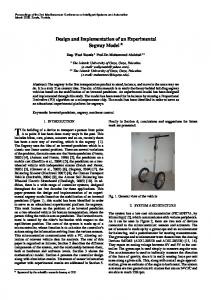
List of Figures 1.1
Schematic representation of the PV drive system, indicating interactions between various subsystems. . . . . . . . . . . . . . . . . . . . . . . . . . . . . . 12
2.1
Schematic representation of the PV drive system, indicating interaction tween various subsystems. . . . . . . . . . . . . . . . . . . . . . . . . . . Variable speed drive . . . . . . . . . . . . . . . . . . . . . . . . . . . . . Separate compressor and motor cooling system, including a condenser . .
2.2 2.3 3.1 3.2 3.3 3.4 3.5 3.6 3.7 3.8 3.9 3.10 3.11 3.12 3.13 3.14
be. . . 13 . . . 17 . . . 19
Schematic representation of the PV-drive system, indicating interaction of the DC-DC converter between subsystems . . . . . . . . . . . . . . . . . . . . . The boost converter topology . . . . . . . . . . . . . . . . . . . . . . . . . . A two-phase interleaved boost converter with coupled inductors . . . . . . . Z-source converter . . . . . . . . . . . . . . . . . . . . . . . . . . . . . . . . Clamp mode coupled-inductor buck-boost converter . . . . . . . . . . . . . . Non-isolated boost converter with a high voltage gain for non-isolated on-line UPS . . . . . . . . . . . . . . . . . . . . . . . . . . . . . . . . . . . . . . . . Full-bridge converter: Center-tap connected half bridge diode rectifier . . . . Rectifier configuration: Half-bridge diode rectifier . . . . . . . . . . . . . . . Full-bridge converter: Full-bridge diode rectifier . . . . . . . . . . . . . . . . Soft-switching Full-bridge Converter . . . . . . . . . . . . . . . . . . . . . . Isolated full-bridge boost converter with voltage doubling rectifier . . . . . . The push-pull converter topology . . . . . . . . . . . . . . . . . . . . . . . . The series-loaded resonant DC-DC converter . . . . . . . . . . . . . . . . . . Resonant Push-Pull converter: which include active clamp circuits and a voltage doubler . . . . . . . . . . . . . . . . . . . . . . . . . . . . . . . . . . . .
4.1
Schematic representation of the PV-drive system, indicating interaction between subsystems . . . . . . . . . . . . . . . . . . . . . . . . . . . . . . . . . 4.2 Resonant Push-Pull converter . . . . . . . . . . . . . . . . . . . . . . . . . . 4.3 Mode 1 of the non-overlapping operation . . . . . . . . . . . . . . . . . . . . 4.4 Mode 2 of the non-overlapping operation . . . . . . . . . . . . . . . . . . . . 4.5 A current summation of the resonant capacitor currents making up the secondary winding current . . . . . . . . . . . . . . . . . . . . . . . . . . . . . . 4.6 Mode 3 of the non-overlapping operation . . . . . . . . . . . . . . . . . . . . 4.7 Inductor voltage over a half period operating below 50 %duty cycle . . . . . 4.8 Non-overlapping control and power signals . . . . . . . . . . . . . . . . . . . 4.9 Mode 1 of the overlapping operation . . . . . . . . . . . . . . . . . . . . . . 4.10 Mode 2 of the overlapping operation . . . . . . . . . . . . . . . . . . . . . . 4.11 Mode 3 of the overlapping operation . . . . . . . . . . . . . . . . . . . . . .
xi
. . . . .
20 26 26 27 28
. . . . . . . .
29 30 30 31 32 33 34 35
. 36 . . . .
37 38 40 40
. . . . . . .
41 43 45 46 47 48 49
Stellenbosch University https://scholar.sun.ac.za
LIST OF FIGURES
xii
4.12 4.13 4.14 4.15 4.16 4.17 4.18 4.19 4.20 4.21 4.22 4.23 4.24 4.25 4.26 4.27 4.28 4.29 4.30 4.31 4.32 4.33 4.34 4.35 4.36 4.37 4.38 4.39 4.40
50 51 58 60 62 62 62 63 63 63 64 64 64 65 65 65 66 67 67 67 68 68 68 69 69 69 69 69
4.41 4.42 4.43 4.44 4.45 4.46 4.47 4.48 4.49 4.50 4.51 4.52 4.53 4.54 4.55 4.56 4.57 4.58
The voltage across the inductor for a half period, the overlapping operation . . Overlapping control and power signals . . . . . . . . . . . . . . . . . . . . . . The center-tap transformer, indicating the number of turns . . . . . . . . . . . Integration of converter with the additional circuitry . . . . . . . . . . . . . . The switch current of S1 at 35 %duty cycle . . . . . . . . . . . . . . . . . . . The switch current of S1 at 50 %duty cycle . . . . . . . . . . . . . . . . . . . The switch current of S1 at 65 %duty cycle . . . . . . . . . . . . . . . . . . . The switch current of S1 at 35 %duty cycle . . . . . . . . . . . . . . . . . . . The switch current of S1 at 50 %duty cycle . . . . . . . . . . . . . . . . . . . The switch current of S1 at 65 %duty cycle . . . . . . . . . . . . . . . . . . . The switch current of S3 at 35 %duty cycle . . . . . . . . . . . . . . . . . . . The switch current of S3 at 50 %duty cycle . . . . . . . . . . . . . . . . . . . The switch current of S3 at 65 %duty cycle . . . . . . . . . . . . . . . . . . . The switch current of S3 at 35 %duty cycle . . . . . . . . . . . . . . . . . . . The switch current of S3 at 50 %duty cycle . . . . . . . . . . . . . . . . . . . The switch current of S3 at 65 %duty cycle . . . . . . . . . . . . . . . . . . . Schematic view of the gate-drive circuitry . . . . . . . . . . . . . . . . . . . . Schematic view of the measurement circuitry . . . . . . . . . . . . . . . . . . . Schematic view: The resonant push-pull converter in Altium . . . . . . . . . . Digital view: The resonant push-pull converter in PCB Altium . . . . . . . . . Photo: The resonant push-pull inductor . . . . . . . . . . . . . . . . . . . . . Photo: The resonant push-pull transformer with only one winding, disassembled Photo: The resonant push-pull transformer with only one winding, assembled Top view of the resonant push-pull converter . . . . . . . . . . . . . . . . . . . Photo: The resonant push-pull converter from the right side . . . . . . . . . . Photo: The resonant push-pull converter from the left side . . . . . . . . . . . Photo: The resonant push-pull converter from the back . . . . . . . . . . . . . Photo: The resonant push-pull converter from the front . . . . . . . . . . . . . The measured output voltages against to the measured input voltages under load (less than 300 W) at various duty cycles . . . . . . . . . . . . . . . . . . The measured output voltages against the measured input voltages under noload at various duty cycles . . . . . . . . . . . . . . . . . . . . . . . . . . . . . Comparison of output voltage measured from MCU and Multi-meter . . . . . Comparison of output voltage measured from MCU and Multi-meter . . . . . Comparison of output voltage measured from MCU and Multi-meter . . . . . Comparison of input voltage measurements from MCU and Multi-meter . . . . Comparison of input voltage measurements from MCU and Multi-meter . . . . Comparison of input voltage measurements from MCU and Multi-meter . . . . Comparison of input current measurements from MCU and Multi-meter . . . . Comparison of input current measurements from MCU and Multi-meter . . . . Comparison of input current measurements from MCU and Multi-meter . . . . Comparison of output current measurements from MCU and Multi-meter . . . Comparison of output current measurements from MCU and Multi-meter . . . Comparison of output current measurements from MCU and Multi-meter . . . Inductor voltage: Input voltage of 60 V at 65 %duty cycle. . . . . . . . . . . Inductor voltage: Input voltage of 60 V at 50 %duty cycle. . . . . . . . . . . Inductor voltage: Input voltage of 60 V at 35 %duty cycle. . . . . . . . . . . Diode voltage: Input voltage of 50 V at 35 %duty cycle. . . . . . . . . . . . . Diode voltage: Input voltage of 50 V at 50 %duty cycle. . . . . . . . . . . . .
70 70 71 71 71 72 72 72 73 73 73 74 74 74 75 75 75 76 76
Stellenbosch University https://scholar.sun.ac.za
xiii
LIST OF FIGURES
4.59 Diode voltage: Input voltage of 50 V at 65 %duty cycle. . . . . . . . . . . . . 4.60 Capacitor clamp voltage: Input voltage of 55.7 V and 4.4 A from the PV source 4.61 Capacitor clamp voltage: Input voltage of 60 V and 9.8 A from the Controlled source . . . . . . . . . . . . . . . . . . . . . . . . . . . . . . . . . . . . . . . . 4.62 Capacitor clamp voltage : Input voltage of 80 V and 14.8 A from the Controlled source . . . . . . . . . . . . . . . . . . . . . . . . . . . . . . . . . . . . . . . . 4.63 Efficiency: Measured with input voltage 80 V and 550 V output voltage and measured with input voltage 50 V and 550 V output voltage . . . . . . . . . . 5.1 5.2 5.3 5.4 5.5 5.6 5.7 5.8 5.9 5.10 5.11 5.12 5.13 5.14 5.15 5.16 5.17 6.1 6.2 6.3 6.4 6.5 6.6 6.7 6.8 6.9 6.10 6.11 6.12 6.13 6.14 6.15 6.16 6.17
Schematic representation of the PV-drive system, indicating an interaction between subsystems. . . . . . . . . . . . . . . . . . . . . . . . . . . . . . . . Schematic representation of the control module. . . . . . . . . . . . . . . . . The control module. . . . . . . . . . . . . . . . . . . . . . . . . . . . . . . . Daisy chain connection of master and slave devices . . . . . . . . . . . . . . The basic MODBUS RTU message structure . . . . . . . . . . . . . . . . . . Control loop: Verification of input voltage. . . . . . . . . . . . . . . . . . . . Control loop: Voltage control (Part 1). . . . . . . . . . . . . . . . . . . . . . Control loop: Voltage control (Part 2). . . . . . . . . . . . . . . . . . . . . . Control loop: Load or speed control. . . . . . . . . . . . . . . . . . . . . . . Control loop: Maximum power point tracking (Part 1). . . . . . . . . . . . . Control loop: Maximum power point tracking (Part 2). . . . . . . . . . . . . Control loop: Speed adjustment (Part 1). . . . . . . . . . . . . . . . . . . . . Control loop: Speed adjustment (Part 2). . . . . . . . . . . . . . . . . . . . . Control loop: Shutdown. . . . . . . . . . . . . . . . . . . . . . . . . . . . . . Output voltage transient: Start up at the light-load condition. . . . . . . . . Output voltage transient: Start-up at the no-load condition. . . . . . . . . . Output voltage transient: The voltage regulation with light load changes after start-up. The magnification indicates the load connection. . . . . . . . . . . Schematic representation of the PV drive system, indicating interaction between various subsystems . . . . . . . . . . . . . . . . . . . . . . . . . . . . Photo: The Yokogawa digital power meter. . . . . . . . . . . . . . . . . . . . Photo: The PV panels used as the input source. . . . . . . . . . . . . . . . . Photo: The AVR debugger. . . . . . . . . . . . . . . . . . . . . . . . . . . . Photo: The extra airflow fan. . . . . . . . . . . . . . . . . . . . . . . . . . . Photo: The multi-meters. . . . . . . . . . . . . . . . . . . . . . . . . . . . . Photo: The control module. . . . . . . . . . . . . . . . . . . . . . . . . . . . Photo: The resonant push-pull DC-DC converter is shown plugged in. . . . . Photo: The VSD. . . . . . . . . . . . . . . . . . . . . . . . . . . . . . . . . . Photo: The whole built setup. . . . . . . . . . . . . . . . . . . . . . . . . . Photo: Power sources and oscilloscopes. . . . . . . . . . . . . . . . . . . . . Photo: The front view of the industrial fan. . . . . . . . . . . . . . . . . . . Photo: The induction motor used to run the fan. . . . . . . . . . . . . . . . Photo: The industrial fan, used as a load. . . . . . . . . . . . . . . . . . . . Photo: The industrial fan and induction motor, a side view . . . . . . . . . . Output voltage transient: Start-up of the system increasing the speed to maximum load, in the morning. . . . . . . . . . . . . . . . . . . . . . . . . . . . Output voltage transient zoomed in: Start-up of the system increasing the speed to maximum load, in the morning. . . . . . . . . . . . . . . . . . . . .
. . . . . . . . . . . . . . . .
76 77 77 77 78 79 80 81 85 85 90 91 92 93 94 94 95 96 97 98 98
. 98 . . . . . . . . . . . . . . .
99 101 101 101 102 102 102 103 103 103 104 104 104 104 104
. 105 . 105
Stellenbosch University https://scholar.sun.ac.za
xiv
LIST OF FIGURES
6.18 Output current transient: Start-up of the system increasing the speed until maximum load, in the morning. . . . . . . . . . . . . . . . . . . . . . . . . . 6.19 Output voltage transient: Start-up of the system increasing the speed until maximum load, in the afternoon. . . . . . . . . . . . . . . . . . . . . . . . . 6.20 Output voltage transient zoomed in: Start-up of the system increasing the speed until maximum load, in the afternoon. . . . . . . . . . . . . . . . . . . 6.21 Output current transient: Start-up of the system increasing the speed until maximum load, in the afternoon. . . . . . . . . . . . . . . . . . . . . . . . . 6.22 The PV drive system is operated throughout a day. . . . . . . . . . . . . . .
. 105 . 106 . 106 . 106 . 107
B.1 Photo: The resonant push-pull inductor . . . . . . . . . . . . . . . . . . . . . 115 C.1 C.2 C.3 C.4 C.5 C.6
Control Control Control Control Control Control
signals: signals: signals: signals: signals: signals:
35 50 65 35 50 65
%Duty %Duty %Duty %Duty %Duty %Duty
cycle . . . . . . . . . . . . . . cycle . . . . . . . . . . . . . . cycle . . . . . . . . . . . . . . cycle dead-time between S1 and cycle dead-time between S1 and cycle dead-time between S1 and
. . . . . . . . . . . . . . . . . . . . . . . . S3 . . . . . S3 . . . . . S3 . . . . .
. . . . . .
. . . . . .
. . . . . .
116 117 118 119 119 119
Temperature distribution: The diodes heatsinks at 47.9 degrees Celsius. . . . . Temperature distribution: The transformer windings at 47.2 degrees Celsius. . Temperature distribution: The transformer windings at 79.2 degrees Celsius . . Temperature distribution: The transformer windings at 76.4 degrees Celsius . Temperature distribution: The converter. . . . . . . . . . . . . . . . . . . . . . Temperature distribution: Heatsinks. . . . . . . . . . . . . . . . . . . . . . . . Temperature distribution: Heatsinks, with temperature of left heatsink as 68.8 degrees. . . . . . . . . . . . . . . . . . . . . . . . . . . . . . . . . . . . . . . . E.8 Temperature distribution: Heatsinks, with temperature of right heatsink as 60.7 degrees. . . . . . . . . . . . . . . . . . . . . . . . . . . . . . . . . . . . . .
122 122 122 122 123 123
123
F.1 F.2 F.3 F.4 F.5 F.6
124 125 126 127 128 129
E.1 E.2 E.3 E.4 E.5 E.6 E.7
Control Control Control Control Control Control
loop: loop: loop: loop: loop: loop:
Verification of input voltage. . . Voltage control. . . . . . . . . . Load or speed control. . . . . . Maximum power point tracking. Speed adjustment. . . . . . . . Shutdown. . . . . . . . . . . . .
. . . . . .
. . . . . .
. . . . . .
. . . . . .
. . . . . .
. . . . . .
. . . . . .
. . . . . .
. . . . . .
. . . . . .
. . . . . .
. . . . . .
. . . . . .
. . . . . .
. . . . . .
. . . . . .
. . . . . .
. . . . . .
123
G.1 Schematic representation of the PV drive system, indicating interaction between various subsystems . . . . . . . . . . . . . . . . . . . . . . . . . . . . . 131 H.1 Output voltage transient zoomed in: Start-up of the system increasing speed until maximum load, in the morning - Attempt 1. . . . . . . . . . H.2 Output voltage transient zoomed in: Start-up of the system increasing speed until maximum load, in the morning - Attempt 2. . . . . . . . . . H.3 Output voltage transient zoomed in: Start-up of the system increasing speed until maximum load, in the morning - Attempt 3. . . . . . . . . . H.4 Output voltage transient zoomed in: Start-up of the system increasing speed until maximum load, in the morning - Attempt 4. . . . . . . . . . H.5 Output voltage transient zoomed in: Start-up of the system increasing speed until maximum load, in the morning - Attempt 5. . . . . . . . . .
the . . the . . the . . the . . the . .
. 132 . 132 . 133 . 133 . 133
Stellenbosch University https://scholar.sun.ac.za
xv
LIST OF FIGURES
I.1 I.2 I.3 I.4 I.5
Output voltage transient zoomed in: Start-up of the system increasing speed until maximum load, in the morning - Attempt 1. . . . . . . . . . Output voltage transient zoomed in: Start-up of the system increasing speed until maximum load, in the afternoon - Attempt 2. . . . . . . . . . Output voltage transient zoomed in: Start-up of the system increasing speed until maximum load, in the afternoon - Attempt 3. . . . . . . . . . Output voltage transient zoomed in: Start-up of the system increasing speed until maximum load, in the afternoon - Attempt 4. . . . . . . . . . Output voltage transient zoomed in: Start-up of the system increasing speed until maximum load, in the afternoon - Attempt 5. . . . . . . . . .
the . . the . . the . . the . . the . .
. 134 . 134 . 135 . 135 . 135
Stellenbosch University https://scholar.sun.ac.za
List of Tables 2.1
Basic electrical design parameters . . . . . . . . . . . . . . . . . . . . . . . . . 18
5.1 5.2
Speed adjustments for different speed ranges . . . . . . . . . . . . . . . . . . . 89 Speed adjustments for different speed ranges . . . . . . . . . . . . . . . . . . . 89
xvi
Stellenbosch University https://scholar.sun.ac.za
Chapter 1 Introduction 1.1
Hunger and food insecurity
Food insecurity is an outcome of inadequate access to safe and nutritious food necessary for normal development and growth, resulting in chronic undernourishment and hunger. Between 2014 and 2016, an estimated 795 million people across the globe were determined to be undernourished. Most of the affected people were living in developing regions. Increased food availability, accessibility, quality sufficiency and quantity are required to ensure positive nutritional outcomes and long-term food security. Good nutrition plays a vital role in human development; people who receive adequate nutrition are more likely to realize their potential and seize existing opportunities. Furthermore, good governance and political stability create an environment conducive to food security. [1]. Central to the fight against hunger is economic growth-socio-economic elements that enable food security include economic growth, agricultural productivity, and social protection. Thus, due to a higher wage threshold, higher unemployment rate and labor demand, richer countries are less susceptible to food insecurity [1]. Social protection systems and programmes that focus on nutrition, health, and education as well as distribution schemes that promote food security plays a vital role in the fight against hunger. Public policies support the management of food resources and implementation of correct practices and techniques . Improved agricultural productivity plays a key role in increasing food availability and thus improving food security. As agricultural productivity increases, more food is grown. As a result, farmers become more competitive and can generate more income. Higher productivity reduces the price of staple foods and thus increases access to basic food items [1]. In addition, when small-holder and family farmers have the opportunity to sell food at markets, this facilitates the movement of food from surplus to deficit areas, thus ensuring food availability. When food is sold at markets, price signals are transmitted to farmers, giving them indications of how to adjust their production. Not only do farmers selling produce rely on markets to make an income, buyers rely heavily on these markets as a source of affordable food. Improving access to marketing opportunities can have a positive impact on productivity [1]. Small-holder agriculture and family farming are central to reducing poverty and hunger [2]. The majority of poor and hungry people in the developing world reside in rural areas. In 2011, the International Labour Organisation (ILO) stated that this figure is nearly eight out of ten people [3]. Growth in small-holder agriculture and family farming has positive effects on economic and nutritional development in these rural areas [2].
1
Stellenbosch University https://scholar.sun.ac.za
CHAPTER 1. INTRODUCTION
2
However, food insecurity is one of the outcomes of consumers demanding more food than producers are able to supply. Abdalla (2007) highlights the importance of mobilizing agriculture to rapidly increase food production to meet the growing population needs. He also mentions the value of improving the integration of public, private and informal actors to enable better food security services to the needy with appropriate food pricing schemes and policies. Food availability is negatively affected by problems within the agricultural supply chain. Recurring low productivity and frequent natural disasters contribute to frustration in the supply chain Issues in the spectrum of demand are related to a lack of food entitlement (poverty), because of weak economic growth; irregular and poor balanced income; unemployment; failure in proper governance and failure to manage supply. Other factors further complicating the fight against hunger are rapidly growing populations, diseases (such as HIV) and constraints in implementation (lack of financial resources) [4]. Technological developments, promotion of agriculture and rural development have a positive impact on the productivity of small-holder farmers and thus poverty reduction. Most of the poor live in rural areas and use agricultural and rural activities as a basis for their livelihoods and depend on the agricultural sector for their income. Therefore, agricultural and rural development is vital to achieving economic growth [5].Most people who are undernourished live in Asia and Africa, and their food security depends on agricultural production and income [4]. It is therefore arguable that "agricultural development by small farmers in conjunction with policies to enhance the capabilities of the poor to access food, offers the best hope of a swift reduction in mass poverty and hunger" [5]. Although the world produces enough food to feed its entire population of seven and a half billion people, there are still one in eight people that live in hunger. The World Food Programme (WFP) highlights the following as the main causes of hunger [6]: • The poverty trap, which is a situation where people living in poverty experience its negative effects in a recurring cycle because they cannot afford certain necessities. These necessities include food and tools. The inability to buy food or tools for work hinders the development of a person living in poverty. This hindrance leads to physical weakness and an inability to earn an income that could help them escape poverty and hunger. • Lack of investment in agriculture, including lack of infrastructure particularly in developing countries which limits yield and accessibility to food. Investment in agriculture is effective in the reduction of hunger. • Climate and weather, in the form of natural disasters (droughts, floods, and storms) can have negative consequences for the hungry in developing countries. • War and displacement conflicts disrupt farming and food production. As fighting forces people to flee, they need to find food while displaced from their homes. • Unstable markets, wherein the instability of food prices make it difficult for the poor to access food. • Lastly, food wastage contributes to hunger as one-third of all food produced is never consumed. This means that resources that are used in producing food that is not consumed are wasted. This leads to the unnecessary addition of greenhouse gases to the atmosphere, which has consequences for the climate and, ultimately, for food production. Food waste is further investigated in the following section.
Stellenbosch University https://scholar.sun.ac.za
CHAPTER 1. INTRODUCTION
1.2
3
Food waste
Globally, it was recorded that 40% of food produced was lost before it reached the markets. Lack of refrigeration technology and sustainable energy sources contributes to crops going to waste post-harvest. Insufficient refrigeration contributes to economic loss specifically to small-scale farmers who lose produce and income. Therefore, there is an urgent need to develop refrigeration systems with a focus on cost-effective design and implementation for small-scale farming communities [7]. Furthermore, fresh produce can spoil in hot climates, due to poor storage facilities and lack of cooling infrastructure [8]. Therefore, there is a need to explore and develop alternatively-powered cold-storage for rural communities.
1.3 1.3.1
Cooling Food refrigeration
Refrigeration is significant for the food industry. Refrigeration allows preservation and storage of perishable products until they are sold [9]. Cooling slows down the chemical reactions and breakdown by bacteria. The bacteriological nature of food spoilage was determined by Pasteur [10] and others in the midnineteenth century. To reduce the amount of free moisture leading to bacterial activity, produce must be stored at below the minimum temperature for growth of micro-organisms [9]. Evaporative cooling impacts the temperature and weight of warm produce. When cooling warm produce, temperature and humidity related control methods need to be carefully considered, as freezing or cooling produce does not produce any improvements. When refrigerated, the product will be kept near the condition it was in before it entered the cooling process. Therefore, refrigeration keeps produce fresher for longer and prevents wastage by preservation in cold stores [9].
1.3.2
Solar-cooling
There exists a link between peak solar gain and peak cooling demand. It is therefore possible to produce cooling which coincides with the demand thereof by using solar energy. Solar-powered cooling, applied in this manner, is a potential technology for domestic, commercial and industrial buildings [11]. Solar cooling is a technology using solar radiation energy to provide a cooling application. There are typically three parts to a solar cooling scheme; a means to harness the energy of the sun, a plant to produce cooling and a process of heat rejection [11]. The need for solar-powered cooling systems exists as many buildings in hotter climates require cooling. Low-energy sustainable cooling applications are needed as an alternative to traditional methods. Cooling systems using solar thermal and solar photovoltaic (PV) energy have been presented by Best [12] and Maidment [11]. Solar thermal powered cooling is used to energize absorption cycles and solar PV powered cooling is used in vapor, compression refrigeration cycles. The use of these system results in having a low or zero reliance on grid-networks [12]. PV-compression systems drive vapor compression refrigeration systems through the direct current (DC) electricity converted from solar radiation. The DC power produced
Stellenbosch University https://scholar.sun.ac.za
CHAPTER 1. INTRODUCTION
4
is inverted to AC to produce shaft power for a electromechanical compressor. Although PV has efficiency-limitations, according to Best and Pilatowski, these systems are good options due to the lower cost and higher coefficient of performance (COP) of cooling systems, although PV has efficiency-limitations [12]. The Solaire project achieved results that presented promise in creating a viable cooling system. In the project, a 1.2 kW array was used to power a 1 kW prototype air-conditioner. Satisfactory results were achieved for various climatic conditions and food products [11]. In a study funded by the European Union, it was stated that there is significant potential for solar cooling technology in the capacity range of less than 20 kW. The study investigated current and future potential, creating a database of installed application and implementations [11].
1.3.3
Compressors
In the refrigeration cycle, four parts are present, namely evaporation, expansion, condensation and compression. Compression is the one part of the refrigeration cycle that remained a key focus as the drive system will be directly connected to the compressor. The purpose is to compress low-pressure gas from the evaporator and raise it to a highpressure suitable for the condenser [13]. There are two main types of compressor configurations, namely positive displacement, and dynamic compressors. In positive displacement compressors, the pressure increase is achieved by physically reducing volume. In dynamic compressors, the velocity is increased and decreased in a way that changes pressure and the temperature [14]. There are millions of hermetic compressors in domestic refrigerators and freezers, with sizes ranging up to tens of kW. Below a power range of 5kW, single-phase motors, instead of three-phase motors, are used in locations where there is no availability of three-phase supply. There are three different ways to enclose compressors namely open, semi-hermetic and fully-hermetic compressors [14]. The semi-hermetic compressors have extended crankshafts integrated with the rotor of the drive motor. The drive motor stator is fitted within the extended crankcase. Semihermetic compressors are built in a wide range of sizes for both commercial and industrial markets [14]. While semi-hermetic compressors are still manually accessible, inaccessible fully-hermetic compressors also exist. The motor and compressor are sealed within a steel shell; this restricts access for repair or maintenance. Fully-hermetic compressors operate at a twopole synchronous motor speed, usually 2900 rpm for a 50 Hz supply. Semi-hermetic run at a four-pole speed of 1450 rpm [14]. Using a variable speed drive (VSD) provides speed variability in a controllable way and speed limitations can be maintained using this control. The large start currents are reduced or mitigated by the rotationally slow starting and gradual speed increase of the VSD controlled shaft [14]. DC motors are used for small compressors. AC to DC conversion is required when using the grid as an input source. Frequency differs across countries; the DC motor is universally suitable because the frequency is not limited. There is a need for small compressors driven by low-voltage DC supplies. Typical cases include batteries or solar cells, where there is grid electricity, for small boats or mobile homes [14]. The failure of a motor within an enclosed system may damage other vital components. This may lead to products decomposing and serious contamination of the system. However, protective devices can be fitted to mitigate this risk [14].
Stellenbosch University https://scholar.sun.ac.za
CHAPTER 1. INTRODUCTION
5
Open compressors have a shaft extended from the crankcase to external drive capability using motors. Open compressors require a gland or a seal. When ammonia is used as a refrigerant, open-drive compressors are required because ammonia is not compatible with copper wiring and/or components. Coupling with the compressor may be direct to the shaft of the motor or via a belt drive. The shaft seal usually comprises a rotating ring of carbon with a highly polished metal facing ring, with the whole assembly being well lubricated. The carbon ring is spring loaded to allow for slight movement of the shaft [14].
1.4
Solar PV as an Energy source
Conversion from sunlight to electricity is completed using PV semiconductor materials, in most cases, pure crystalline silicon is used. They are called PV because of the ability of these semiconductor materials to convert the energy contained in photons of light into electrical energy [15]. In developed countries, the deployed PV systems are based on grid-connected topologies since the grid is very stable. For developing countries, this is not the case, where the grid is intermittent or some of the population have no connection to the grid. This is the reason renewable off-grid solutions are sought after [16]. The main reasons behind the search for alternative energy solutions are increasing power requirements and demands, the high cost of fossil fuels and the environmental impact of their use in generating electricity. It is for these reasons that the development of sustainable and affordable energy resources that are not harmful to the environment remains imperative [16]. The use of PV as a source of electricity for rural areas is a favorable alternative to the national grid. PV off-grid systems are essential for rural electrification. The following factors contribute toward the support of small-scale generation: accessibility, load demand, the fight against poverty and leapfrogging [17]. • Accessibility: Renewable small-scale generation is preferred for remote areas that, due to the unfeasible costs involved remain unreachable by the main, national grid [18]. • Load demand: The demand load in rural areas is very low, thus a small-scale system is more suitable [19]. • The fight against poverty: The continued focus on poverty-based strategies drew attention to probable links between energy and poverty which underlines the importance of improving living conditions through energy services. Electricity was thus considered as the main component in programmes geared towards rural development, using scale-small generation as the preferable option [20]. • Leapfrogging: Learning from what has already been done, rural areas can implement and incorporate the most advanced technologies for electrification [21]. Leapfrogging entails the observation of successful technological implementation, incorporating the advanced implementation stages while skipping earlier stages of unsuccessful advancement. PV small-scale generation is one such example [22]. Adding to the background of the study, the following points outline various applications and systems in which the PV-source has been used. The components and concepts
Stellenbosch University https://scholar.sun.ac.za
CHAPTER 1. INTRODUCTION
6
used in some of these applications, specific to the proposed cooling application, are included in the following chapter. PV has been used for electrification, solar-cooling, water pumping and small-scale off-grid systems for households and is discussed more in depth in the following sections: • Off-grid Electrification using Solar PV in a rural area in Malaysia Researchers, M. Fahmi and D. Isa et al, implemented the use of PV energy systems for rural households. It is essential that further research is conducted in order to discover and develop innovative technologies to extract the maximum solar energy to be used to fulfill demands. A 2 kW system was implemented in the form of a solar off-grid cabin. The investigation was conducted into the possible replacement of current diesel generators with PV systems to supply power to houses in rural areas. All the usual household power-needs were combined and designed to be supplied for by the PV system. The PV system comprised of panels, a charge controller, an inverter, sensors and an electronic-load. The total load used, representing the household power-need, was implemented by using an electronic-programmable load. The system was tested for 3 days against the average rural household. The researchers concluded that the system was able to supply sufficient power to the rural household [23]. • Off-grid Electrification using Solar PV in a rural area as an affordable solution in Sub-Saharan Countries The financial feasibility of implementing an off-grid PV system for rural areas was investigated. The study was conducted for the Sub-Saharan African (SSA) area. In 2012, the percentage of people without access to electricity in SSA was 35.3%. Five major issues were investigated, namely cost-effectiveness, affordability, financing, environmental impact and poverty alleviation [24]. Diesel generators are most frequently used as they are conventional and low cost compared to solar PV. They have greater reliability and provide income-generating possibilities from the electricity produced [24]. The initial investment of a 100 W solar PV system could be alternatively spent on a 1.2 kW diesel generator. Diesel generators have higher running costs, but as stated, the generated electricity could be used for activities such as water pumping, milling, and irrigation or income generating activities [24]. However, the main reason consumers from rural areas cannot afford a solar PV system is due to their inability to pay the credit whilst burdened with the strain of operations and maintenance costs. Authors S. Baurzhan and G. Jenkins concluded that off-grid solar PV systems for rural communities of SSA would not be financially feasible unless entities from abroad are to subsidize them [24]. Authors outline two important advantages that PV systems have over diesel generators. PV is less detrimental to the environment than diesel generators. Furthermore, the cost of PV systems will eventually drop below that of diesel generators as the cost of PV systems is decreasing annually[24]. • Solar PV used in small-scale power systems The design an off-grid 2 kW solar PV system was designed by Bouzguenda and Omair et al, from King Faisal University in Saudi Arabia. Their study presented
Stellenbosch University https://scholar.sun.ac.za
CHAPTER 1. INTRODUCTION
7
the potential use of solar PV and a successful design methodology. They concluded that high ambient temperatures and shading losses reduced system performance [25]. The study was done in Saudi Arabia where according to figures given by Chatham house, approximately 70% of the energy consumption goes to air conditioning [26]. Bouzguenda and Omair et al, state that the reason why air-conditioning constitutes such a high percentage of energy consumption is that of cooling-unit inefficiency coupled by the frequent use of cooling units in the summer during which there are very high temperatures [25]. A stand-alone solar PV system was designed and presented with a proposed methodology for technical and economic analysis. The system was sized to 2 kW and the design-methodology was based on five stages. These included power needs, followed by the PV system type and the specific surroundings, a shading analysis and system layout and sustainability constraints [25]. Finally, an economic analysis was conducted based on the aforementioned stages. The design and methodology were implemented with energy storage. The focus of the study was on the specific geographical site, shading, and cost [25]. Qaiser et al [16] proposed the design and implementation of a low-cost, efficient and robust maximum power point tracking (MPPT) based charge controller that is suited for stand-alone or backup PV applications for small power-levels. The converter used a microcontroller. The paper focused on the charge controller. The charge controller did maximum power point tracking and charged the batteries. A Buck-boost topology charge controller was implemented because the topology is easily implemented and has simplified control. The implementation was found to be successful as it was tested through charging batteries at various voltages with good results [16]. • Solar PV used in pumping applications Economic analysis of Photovoltaic powered water pumping and desalination without energy storage for agriculture The economic feasibility of battery-less PV water pumping and desalination systems was investigated and modeled using simulations. The simulation was performed hourly, simulating PV pumping and desalination at variable loads [27]. Solar PV was compared to other energy sources such as diesel and the grid. Multiple inverter topologies were simulated as well. The economic analysis results showed that solar PV based systems fared better for water pumping than diesel-based systems. However, economically grid-based systems fared even better than PV based systems due to electrical costs [27]. PV water pumping has been investigated and proves to be technically feasible to operate with commercial systems. Jones et al evaluated medium to large-scale, variable speed, directly coupled with PV pumping and desalination systems. PV array sizes ranged from 15 to 120 kW for pumping and desalination systems. Compared to previous studies, larger-scale simulated system sizes, along with system optimization resulted in a cost reduction in PV- powered systems [27]. The PV systems simulated were without battery banks, thus pumping and desalination would not continue during the night or in low sunlight conditions. Therefore,
Stellenbosch University https://scholar.sun.ac.za
CHAPTER 1. INTRODUCTION
8
the operation of the systems was adjusted, using an inverter-controller to charge the inverter frequency to suit the available PV power for maximum efficiency and reliability. The adjustments were in speed, flow rate, and pumping head, to match the power available from the PV source [27]. • An Effective Induction Motor Control for Photovoltaic Pumping For the application of PV pumping, Vitorino et al published a paper on effective induction motor control. PV technology is most promising for low-power distributed electrical generation. The decrease in price per peak watt for PV panels is a very attractive feature [28]. In the paper, a battery-less pumping system with PV as input source is proposed as batteries are heavy, expensive and have one-fifth of the lifetime of a PV panel. The PV pump-storage system would store energy as potential energy using water-storage that could be utilized later [28]. The system would be made out of five components, namely the PV panels, a DC-DC converter, a DC-AC inverter, a three-phase induction motor and lastly, a centrifugal pump. This is the general make-up of a PV system, except for the last two components which are application-specific [28]. The induction motor provides the electromechanical power conversion fed by an inverter drive. Sensorless methods are used to maximize the potential energy of water pumped for the available solar energy [28]. • Solar used in cooling applications In recent years the research and development of solar refrigeration technologies have gained global interest because they offer desirable advantages. The first advantage is the alleviation of harmful environmental effects of traditional refrigeration machines. Secondly, the coinciding with solar radiation supply with the regular peak demand in cooling is an advantage previously mentioned [29]. Solar energy can power a refrigeration cycle through its conversion to electricity or heat. In a review conducted by Fan et al, it is stated that more interest has been found in solar thermal-driven refrigeration technologies than in solar photovoltaicdriven refrigeration technologies due to the lower efficiency and fairly high initial cost of the PV system. However, in this project, developments are made regarding photovoltaic-powered refrigeration for small-scale farmer produce using the proposed drive-system, which has implications that will be discussed later [29].
1.5
Introduction to the project
A power conversion system was built to power a cooling system for small-scale farmers. The field of application would be agriculture, specifically powering a cooling system for small-scale farming. The cooling system was powered by PV solar panels. The PV system voltage was increased to a suitable voltage required to power the cooling system Certain voltage level requirements need to be met in order to drive retail cooling systems with VSDs. When using PV panels to power such systems the number of panels needed to build up the voltage level required is extensive and consequently expensive. To decrease the number of panels and expenses required, a DC-DC converter could be designed, built and implemented. The converter is then designed to increase the output
Stellenbosch University https://scholar.sun.ac.za
CHAPTER 1. INTRODUCTION
9
voltage of the system to meet the voltage requirement of the VSD for the cooling system. There are a few problems to discuss in the field of application regarding the project. The major ones are: • Pricing • Voltage level elevation • Implementation of new technology (power electronics) in the field of agriculture. The ability of small-scale farmers to successfully produce and deliver fresh-produce has been negatively affected by a number of factors. One of which is the inability to store fresh produce for a period of time between harvesting and marketing. It has been argued that small-scale farmers lose a substantial percentage of their fresh produce or their income due to an absence of proper cooling facilities. This project forms part of a multidisciplinary effort (along with horticulturists, civil engineers, etc.) to establish affordable cooling facilities that can address this problem.
1.6
Research question
Using the proposed development process, is the design and implementation of off-grid PV drive systems feasible for small-scale farmer fresh produce cooling? This project aims to reveal the necessary requirements for implementing a cost-effective cooling system for small-scale farmers, where many of these farmers are found in rural areas (at least where the supply of energy is restricted or inaccessible). Part of the answer will, therefore, have to address the use of alternative energy sources, with the focus for this study being photovoltaic energy sources. To provide a proper answer the following needs to be considered: • What is necessary for a drive system supplied from photovoltaic energy sources to successfully drive such a cooling and refrigeration system?
1.7
Problem statement
Using the proposed development process, is it feasible to design and implement off-grid PV drive systems for small-scale farmer fresh-produce cooling that is cost-effective?
1.8
Research aims
In order to practically address the research questions above in such a way that the result may be used to practically evaluate cooling and refrigeration systems, the following research aims have been identified: • To design and build a drive system supplied from photovoltaic energy sources for a cooling system requiring a few kilowatt of power. This aim would enable the evaluation of the ability to drive cooling systems and to propose possible improvements or alternative approaches in future.
Stellenbosch University https://scholar.sun.ac.za
CHAPTER 1. INTRODUCTION
10
• To investigate, propose and practically demonstrate the ability to drive commercially available cooling systems for energy supply restricted applications driven by the drive system as expressed in the first aim. This aim will again enable the evaluation of the feasibility of powering cooling systems with PV drive systems and will possibly aid in future research relating to small-scale fresh produce farming. This thesis documents the design and implementation of an off-grid PV drive system for a cooling system. The drive system needs to be able to increase the PV array voltage, so that it is suitable for the application. The project was aimed at small-scale farmers, thus the financial aspect of the project contributed heavily to the direction of the project. Further aims include: • The designing the PV drive system; • elevating the PV array voltage; and • the implementation of cost-effective technology power electronics in the field of agriculture.
1.9
Research objectives
The following research objectives are envisaged to address the research aims: • To design and to implement a DC-DC converter to supply commercial VSD from solar photovoltaic modules. This action arises from the fact that the maximum voltages possible from photovoltaic modules, especially in lower power applications, are not sufficient in the application to drive normal single-phase and three-phase motors as found in off-the-shelf commercially available cooling systems. • To design and to implement a micro-controller based control systems to control the DC-DC converter as well as a VSD to ensure optimal application of energy flow. • To establish a combined system of the various subsystems mentioned above to evaluate and to prepare for application as part of a cooling system. • To adapt a commercially available cooling system for variable drive/energy restricted application and to apply this cooling system as part of an energy restricted application. • To evaluate the entire system in the field as part of a multidisciplinary effort to help address the problems faced by small-scale farmers.
1.10
Significance of the Research
The research was done in the form of a feasibility study. This was done to determine whether the use of off-the-shelf products with a self-built converter, power and control units could be used to implement an off-grid PV drive system able to power a cooling system used in small-scale farming. After designing and implementing the system, feasibility or the lack thereof will be the significance of the research. Any contribution made, in terms of small-scale farming refrigeration drive systems, would ultimately be in aid of alleviating food insecurity and hunger.
Stellenbosch University https://scholar.sun.ac.za
CHAPTER 1. INTRODUCTION
1.11
11
Scope of the Research
The feasibility of the design and implementation of cost-effective PV drive off-grid systems for small-scale farmer, fresh produce cooling will be investigated. A drive system will be built to provide power and control for the application consisting of a DC-DC converter, a control module, and a commercially available VSD. Once manufactured, the system will be tested with PV panels and various loads leading up to the implementation of the cooling system.
1.12
Proposed execution project
In the investigation to determine the feasibility of the implementation of a designed PV drive system, the research methods will be stated for the development process, for rural farming produce cooling. Qualitative research methods will be followed in order to select important parts of the PV drive system. Investigations will be carried out in order to gather information about certain converters and control units (Micro-controllers). The gathered information will be compared in a qualitative manner to determine the most suitable design to implement. Quantitative research methods will be followed, in which off-grid PV system section components need to be defined and designed. These will include theoretical design, simulations of the converter’s theoretical design and measurements of the converter parameters. The results of these methods will be used in the evaluation of the converter design. Manufacturing will commence once Printed circuit boards (PCB) have been designed and populated. Thereafter, a testing phase will begin of the designed electronic circuits (converters and control unit) with various load-conditions and input sources. A second testing phase will be done moving closer to the proposed sources and load conditions until implementation is done with the PV source and cooling-load application. Lastly, observations and measurements of the development and implementation process will be documented.
Stellenbosch University https://scholar.sun.ac.za
12
CHAPTER 1. INTRODUCTION
1.13
Thesis outline
A short description of each of the chapters in this thesis: Chapter 2 gives a high level - detailed overview of the research project Chapter 3 discusses the DC-DC converter and provides a comparative review of various converters. These converters are evaluated according to the stated criteria. In closing, a DC-DC converter choice is made for the project. Chapter 4 describes the hardware design of the chosen DC-DC converter and shows the results of the implemented DC-DC converter. Chapter 5 describes the control of energy-flow of the system. Chapter 6 presents the implementation and application of an experimental system. Chapter 7 concludes the project through the provision of an evaluation and necessary recommendations. Figure 1.1 will be used as a visual indication of the systems involved or being discussed in the relevant chapter. It will be shown at the start of each chapter, highlighting the focused system or systems in black.
PV Source
DC-DC converter
VSD
Cooling system
Control module
Figure 1.1: Schematic representation of the PV drive system, indicating interactions between various subsystems.
Stellenbosch University https://scholar.sun.ac.za
Chapter 2 High-level project overview 2.1
Introduction
This chapter entails a brief layout of the project and provides the research overview. Firstly, the development process of the project is presented in section 2.2. Parts of the research project are discussed namely, the input source in section 2.3 and the drive system section 2.4. The latter, in subsection 2.4.2, expanding on the voltage elevation of the input source. The application of voltage elevation for the project is discussed in section 2.5, which is small-scale farming refrigeration. The project’s main electrical specifications are stated in section 2.6. Lastly, the integration of these parts for the project is outlined in section 2.7. Figure 2.1 illustrates the system and the interaction of subsystems.
PV Source
DC-DC converter
VSD
Cooling system
Control module
Figure 2.1: Schematic representation of the PV drive system, indicating interaction between various subsystems.
This system is aimed at small-scale farming communities, and the detail will be presented in this chapter in subsection 2.5.1. In this section, the system will be discussed and explored from every angle. A holistic overview will be provided, stating the detail of each part of the system from the input source, through to the increase in DC voltage. Thereafter, the chapter will outline the AC-conversion of the DC voltage. Lastly, the cooling system, which is the application for which the increased AC voltage is required, will be discussed. The focus of this chapter was to state the development process followed for the implementation of the PV drive system for small-scale farm produce cooling. This was carried out in order to determine the viability of the process.
13
Stellenbosch University https://scholar.sun.ac.za
CHAPTER 2. HIGH-LEVEL PROJECT OVERVIEW
14
This system contains many crucial parts from the supply through to the load, which will be briefly discussed below. PV was chosen as the input source; the voltage is increased and regulated using a DC-DC converter. With the voltage now elevated to a usable magnitude, the DC voltage is made AC with a VSD. The control module is the central control unit governing system execution, mainly between the DC-DC converter and the VSD. This is done in order to drive an off-grid the cooling system load for small-scale farmers.
2.2
Development process
Smallholder farms face multiple problems, which include limited access to electricity, lack of agricultural technology, lack of adequate produce storage and cooling facilities. The development of technology as a solution to a multiplicity of simultaneous problems is worth investment [30]. This is the focus of the project and the proposed development process. The objective is to verify feasibility for the development a PV drive system for a cooling application aimed at small-scale farmers. This will be completed using the development process followed for this project. The development process entails the use of commercial products (as far as possible) in integration with necessarily designed subsystems to implement the PV drive system. The decisions and their justifications made following this development process will be stated. An evaluation of these decisions and alternatives to negative outcomes thereof will be provided. In order to implement a cost-effective drive system, commercial components were used as far as possible. These commercial components include the PV array and the VSD. The DC-DC converter and the control module were designed and built for use with the commercial components. The converter’s supplementary circuitry includes power, measurement, gate-drive and isolation circuitry. Integration of the system is achieved by having a central control module that monitors and controls the drive system. The control module designed controls the converter and the VSD. The VSD speed is adjusted and the converter output voltage is regulated by Maximum Power Point Tracking (MPPT). These are the two main control objectives forming part of the energy flow from the source to the load. The control module provides other functions as well, for example, measurement of the input and output currents and voltages.
2.3 2.3.1
Input source for the project Introduction
The rural community areas do not have sufficient electricity supply. Reasons for the insufficiency of supply include the intermittency of the electricity grid, the inability of the grid to reach the rural areas and limited access to electricity grid facilities. Governments cannot afford an expansion of their national grids, thus leading to limited access and failure to provide such areas with electricity.
Stellenbosch University https://scholar.sun.ac.za
CHAPTER 2. HIGH-LEVEL PROJECT OVERVIEW
2.3.2
15
Resources for electricity
Conventional grid electricity is generated using resources that may impact the environment negatively. These resources include coal and natural gas and are being used to generate electricity. However, these sources are not renewable, are being depleted and may produce waste harmful to humans [31]. Although well-priced, the use of non-renewable resources for electricity generation for grid networks poses a threat to the environment, with these sources, electricity is mostly provided to urban, near-urban and developed areas where with the electricity grid is reachable. Limited or no access is provided to the rural communities, which need electricity as well. Therefore, an energy source is needed that is mobile, not limited to the reaching range of the conventional grid, affordable and easily replenishable [22]. Renewable energy sources are easily replenished and are not harmful to the environment in their generation of electricity. These sources are used to generate and provide electricity, regardless of access to the grid. These sources use mobile equipment and can provide electricity to rural communities and areas where the conventional grid is unable to reach [22, 31]. These sources are still being improved in terms of technology, cost, and implementation. This makes it a very competitive market, as manufacturers are progressing in developments which reduce cost and pricing [24]. Renewable energy sources that are currently used and researched are wind, solar, pump-storage and many others (geothermal, tide/ocean, Hydroelectric, and biomass). The focus of the proposed development process is solar and specifically solar PV.
2.3.3
Solar PV
To implement solar PV as a source of electricity for rural areas is a viable option as it is easy to set up and able to provide the necessary electricity that rural communities need for certain applications. It does not negatively impact the environment when generating electricity. In terms of solar PV, a substantial amount of physical space is needed for module installation. Solar PV modules have low efficiencies but there is no pollution produced during the generation of electricity [15]. In summary, solar PV is mobile in its setup, making it highly accessible. The source, the sun, is abundant and able to supply the needed electricity through PV, for various applications. Disadvantages of solar PV include high cost and low efficiencies. Major advantages include minimal pollution, the source is naturally renewable and is still being researched and developed, meaning future price drops [[15].Solar PV as input source is a sustainable source of energy as the sun is abundant (with high insolation levels in SSA) [24]. A PV drive system was developed for cooling purposes aimed at rural small-scale farming communities.
2.3.4
Input source specifications
For this project, a medium power level of 1.5 kW was designed for. This power level equates to six 250 W, 35 Vmpp PV panels. The DC-DC converter was designed to operate with an input voltage range of 50 V to 120 V, which could be made up of six panels in certain connection configuration. Certain series and parallel configurations were needed making up this voltage range, for example, 3 strings in parallel of 2 panels each in series.
Stellenbosch University https://scholar.sun.ac.za
CHAPTER 2. HIGH-LEVEL PROJECT OVERVIEW
2.3.5
16
Cost of modules
This starting capital cost of solar PV equipment such as panels can be very intense. The price of a 250 W from Renesola is R 2,625.00 [32]. This is the cost of the PV modules to match the specifications of 550 V and 1.5 kW. Building this power capacity with the above stated 250 W panels, 6 panels are required. This brings the total panel cost of the panels to an estimate of R 15,750.00.
2.3.6
Safety
The use of a few panels, in the correct configuration, provides a relatively small accessible input voltage. This means, that unforeseen contact or accidents with the power source would be relatively harmless and not fatal, as opposed to higher input voltages. The voltage is elevated and applied in a usable manner within the drive-system which would not be accessible.
2.4 2.4.1
Drive system Introduction
The drive system design used contains a self-built combination of a control module and a DC-DC converter, used with a commercially bought VSD. The proposed design features a central control module, which provides integration between the DC-DC converter with the VSD, above many other functions. This allows a controlled voltage input to the VSD from the DC-DC converter using solar PV as the input source.
2.4.2
Voltage Elevation
PV panels are low-voltage sources and are often used for domestic and industrial applications [33]. These applications require higher voltage input sources, which means that there needs to be some sort of voltage increase or voltage elevation from the PV panels to the application, in order to power these applications with a suitable voltage. DC-DC converters are suitable for voltage elevation energy-efficiently. DC-DC converters will be fully discussed in chapter 3. A combination of solar PV with a DC-DC converter provides compatibility and mobility, as the required voltage of the application can be easily achieved while operating in an optimum power range. Without a converter, a matchup of connection configurations (series and parallel connection) is required in voltage and power. To extract maximum power would require a load match at a specific voltage. Therefore, use of a converter is advantageous [15].
2.4.3
Control module
The control module is a central part of the drive system. It provides communication, control of switches, the ability to take in measurements and processing them. These measurements are used to execute the necessary algorithms. This module observes and monitors the output and input voltages and currents. Based on these measurements, the DC-DC converter regulates its output voltage for the VSD. Providing a sufficient voltage as input to the VSD - the VSD speed is controlled by the control module through
Stellenbosch University https://scholar.sun.ac.za
CHAPTER 2. HIGH-LEVEL PROJECT OVERVIEW
17
communication. Basic speed control is implemented. The control module will be discussed in more detail in chapter 5.
2.4.4
Variable speed drive
From the converter, a regulated DC output voltage is supplied. A VSD was chosen, providing a way to integrate the elevated input source voltage with the cooling application, including an option for speed control. It does this by supplying the load, typically a motor, with variable frequency AC power. VSDs take in DC-power or AC-power. This power, whether DC or AC goes through a rectification stage, using diodes. After the power has gone through this rectification stage, it is built up in a capacitor. The voltage built up in this capacitor is called the DCBus voltage. Using this DC-bus voltage and pairs of transistors, an AC output voltage is produced. The frequency of the AC output voltage is adjusted by the VSD, to a user set-frequency. This is done by switching the transistors on or off at specific times. The output of the VSD is perceived by the three-phase motor as a sinusoid with the variable frequency. The VSD does this by modulating the DC-bus voltage through switching the transistors on and off. It produces a sinusoidal output per each phase. The VSD, known as an adjustable-speed motor drive, eliminates power losses by adjusting the motor speed to appropriately supply a variable load. Mohan et al give the example of an adjustable-speed motor drive used with a motor-driven pump. Energy is conserved by not letting the motor run at a constant speed over a time-period for a variable load, but by adjusting the speed [34]. A VSD schematic is shown below in figure 2.2 [35], the input of the diagram could be AC or DC building a DC link when powered. Thereafter, an inversion stage is presented. This inversion stage is used to create a PWM waveform that is controlled and is seen by the motor as sinusoidal.
Figure 2.2: Variable speed drive
. Since VSDs are typically used with three-phase motors two popular motor types exist. These are discussed in Appendix D, including a mention of three-phase systems.
2.5 2.5.1
Cooling application Small scale farming
Smallholder farmers, as defined by V.Barends, are farmers who have low yields, produce more products than is needed for their own consumption and are the direct link with
Stellenbosch University https://scholar.sun.ac.za
CHAPTER 2. HIGH-LEVEL PROJECT OVERVIEW
18
consumers, or supply directly to retail groups who process and market the produce [36]. 84 % of farms worldwide, 570 million farms, operate on less than 2 hectares. This illustrates the role and the importance of the smallholder farmer. In the developing world, these types of small-farms provide income, employment, and food to billions of people [30].people [30]. These same parts of the world house a large fraction of the hungry people in the world. The 500 million smallholder farms in the developing world provide close to 80 % of the produced food in Asia and Africa south of the Sahara. Yet these smallholders are the group that accounts for the poorest and hungry in the world. They live in rural areas and agriculture is the main way to make a living. Therefore, improvement and investment in the development of technologies that will help smallholder farmers are helpful to the people who most need it in the world. Smallholder farmers face many challenges; they are faced with a lack of access to energy and above many other issues, they lack the infrastructure for storage which leads to food loss. Support in these areas will lead to helping and uplifting smallholder farm communities. Supporting such farmers to increase their productivity could lead to the improvement of income, in turn leading to agricultural growth. Providing support for food insecurity increases the ability of smallholder farmers to produce and sell, this enhances their ability to provide nutrition. Their livelihoods can be improved with better access to energy, which is achieved by the promotion and implementation of rural renewable energy use. Lastly, food availability can be improved through investment into storage infrastructure [30]. The proposed product is aimed to contribute to achievement of these outcomes. The project is aimed at smallholder farmers, where the development of a cold storage/cooling system is provided powered by renewable energy. The cooling system is driven by solar PV using a drive system that elevates the panel voltage. This drive system provides control and communication as well, by monitoring outputs.
2.5.2
Refrigeration
The cooling application that this project aims at developing uses a vapor-compression refrigeration system. The system uses a separate compressor and three-phase motor. The compressor and motor are coupled using belts or directly coupled (special couplings) via their shafts. The motor connects to a VSD through which the control of the refrigeration system is provided. Refrigeration systems and such technologies are needed by smallholder farmers, helping them to effectively store and cool produce. The results and implementation of the application will be displayed in chapter 6. In figure 2.3 below, an image of a refrigeration system is shown, containing a condenser at the back and an open compressor and motor coupled using belts.
2.6
Project specifications Table 2.1: Basic electrical design parameters
Parameters
Input voltage range Output voltage range (VSD input voltage) Power
50 V - 120 V 550 V - 600 V 1500 W (Six 250 W PV panels)
Stellenbosch University https://scholar.sun.ac.za
CHAPTER 2. HIGH-LEVEL PROJECT OVERVIEW
19
Figure 2.3: Separate compressor and motor cooling system, including a condenser
In order to power and control a cooling system, the above described electric parameters were to be used as input supply into a VSD, the whole drive system is used in integration with a control module that controls to the VSD and to the DC-DC converter, doing processing on the measurements it monitors. This is the proposed design to power a cooling system driven by PV, for small-scale farmers to cool fresh produce.
2.7
Research project execution
Figure 2.1 illustrates the project in the main system and how the subsystems work together. The input source is a PV array and provides a voltage that ranges from 50 V to 120 V, depending on the configuration of the array and temperature of the module [37]. As seen in the diagram, this input feeds into the DC-DC converter. The DC-DC converter is controlled by the control module, through control signals sent to gate-drivers for the converter switches. The control module measures input and output power by monitoring the converter parameters, able to implement control methods. Control methods to be implemented include maximum power point tracking and voltage regulation. The output of the DC-DC converter is used by the VSD. The VSD is controlled and monitored by the control module and is connected to the cooling system, powering it at optimum power. In the following chapters, the parts will be discussed in more detail, starting with the DC-DC converter in chapter 3.
Stellenbosch University https://scholar.sun.ac.za
Chapter 3 DC-DC converter 3.1
Introduction
This chapter describes the DC-DC converter. A comparison is made between converters investigated for implementation, leading up to the selection of the specifically proposed converter. An overview of DC-DC converters, switch-mode, and resonant converters is discussed in sections 3.2 and 3.3, respectively. The criteria used for the converter choice are stated thereafter in section 3.4. A few converters are chosen, grouped together and then compared. The groups contain basic DC-DC converters, featured in sections 3.5 and 3.6, and resonant converters in section 3.7. In chapter 4, the design and operation of the proposed converter are discussed in-depth. Figure 3.1 shows the system and its interconnection. The main focus of the chapter is the DC-DC converter, highlighted in black.
PV Source
DC-DC converter
VSD
Cooling system
Control module
Figure 3.1: Schematic representation of the PV-drive system, indicating interaction of the DC-DC converter between subsystems
The DC-DC converter plays a key role in the PV drive system. This converter would be used to provide a high voltage output from the lower PV panel voltage, in a safe and controlled manner. The converter should be able to operate within a wide input-voltage range providing a high voltage gain throughout. This should be done cost-effectively and energy-efficiently, which are important factors in order to implement the PV drive system for small scale farming. The feasibility of the proposed PV drive system implementation by small scale farm communities is ultimately investigated.
20
Stellenbosch University https://scholar.sun.ac.za
CHAPTER 3. DC-DC CONVERTER
21
The converter choice was based on the set criteria. The criteria are fully presented later in this chapter in section 3.4. A summary of the criteria to be met to fulfill the requirements of the project are given below as: • A high-voltage gain from low-voltage input, • wide input voltage range, • high efficiency, and • low in cost.
3.2 3.2.1
DC-DC converters: A brief overview Introduction
The advances in power electronics in the last few decades have made it possible to achieve great feats [38]. Previously, such technology has only been used in military and space applications, due to of cost and reliability implications. Since the early 1970s, advances in semiconductor devices led to the switching converter becoming a popular choice [39]. Developments in power electronics in the last 40 years have seen advances in electric motor applications. Motors can now be powered from various sources and at various frequencies [38]. Moreover, the versatility and flexibility in power electronic developments resulted in the development of even newer and better applications. The progress of high-power electronic components has led to an increase in reliability and decrease in cost [38]. Furthermore, rapid population growth and advances in technology have increased electrical power consumption, from 1.5 million MW in 1940 to a projected 5 million MW in 2000 [40]. It is predicted that almost 75 % of the electrical power will be processed by power electronics, about 3.8 million MW in 2000 [40]. The frequent use of power electronics indicates the need for the development of energy and cost-efficient applications, incorporating power electronics such as the DC-DC converter. A DC-DC converter is a device, consisting of electronic and magnetic components, that takes in a certain DC input voltage and produces a certain output voltage. The output is dependent on the device-topology and control. Control is primarily implemented by gate-drivers through transistors and diodes used for conduction of current flow, where desired [34]. These converters often contain inductors and capacitors as filters. These components serve as energy-storage elements in the circuit as well. Similarly, converters can contain transformers, where a greater increase or decrease in the input voltage level to output voltage level is needed [34]. A normal DC-DC converter operation has a DC stage, an AC stage, and another DC stage. The transformer is inserted after the converter’s AC stage. After this AC stage, a rectification stage occurs. For these two stages to take place, the transistor and the diode are used. The transistor is used as a simple switch in the circuit, functioning in both an on-state and an off-state. This provides the AC stage from the DC input, which can then be used by a transformer to scale the voltage. Typically, after this process, rectification is achieved by using diodes in combination with a filter capacitor and filter inductor. From the DC input, through the alternating stage and rectification, a DC output is obtained and changed in voltage level. This is how the DC-DC converter takes one DC voltage level to another, using the described components [34, 39].
Stellenbosch University https://scholar.sun.ac.za
CHAPTER 3. DC-DC CONVERTER
22
Converters can operate in three conduction modes, namely in a continuous-conduction mode, a discontinuous-conduction mode and a boundary-conduction mode which exists between the previous two modes. The continuity (whether discontinuous or continuous) relates to the inductor current flow. However, if the inductor current never reaches zero, the conduction mode is continuous. On the other hand, if the inductor current reaches zero for a duration before the end of the period, its conduction mode is discontinuous. When the inductor current-flow reaches zero precisely at the end of the switching period, the conduction mode is the boundary condition between discontinuous- and continuousconduction [34]. These modes need to be taken into account as they define the design of components for the DC-DC converter.
3.2.2
Elevation factors
The use of DC-DC converters to elevate voltage levels are very useful for applications that need a higher voltage-level powered by low-voltage sources. Using DC-DC converters in conjunction with low-voltage sources, such as PV panels, creates an alternative way of powering commercial or industrial applications. The magnitude of the conversion ratio depends on a few parameters, such as: • The duty cycle; • the transformer winding ratio (if the topology includes a transformer); • the output diode and capacitor configuration; and • lastly, placement of components.
3.2.3
From linear to switching power supplies
DC-DC converters are presented as the main components required for switching power supplies [34]. Therefore, the switching power supply will be investigated in this study, as it is essentially seen as a DC-DC converter. Switching power supplies are able to provide regulation of output voltages, isolation and multiple outputs differing in voltages. Linear power supplies were used traditionally, as it is a power supply using a 50 Hz or 60 Hz transformer and the transistor in its active region [34]. In linear power supplies, a transformer is used providing electrical isolation and delivering output in the desired range. However, the low-frequency transformer is one of the shortcomings of linear power supplies; they are large in size and weight. Another vital shortcoming is the efficiency of the supply that ranges from 30 - 60 %. A significant amount of power loss occurs because the transistor operates in its active region. These supplies do have advantages, for instance, simplicity in circuitry in small power ratings and they do not produce a large electromagnetic interference (EMI). These advantages, unfortunately, do not outweigh the shortcomings, but these shortcomings do lead to a greater appreciation for the switching power supply and the DC-DC converter [34]. The emergence of the switching power supply was due to improvement in the linear supply components and transistor operation methods [34]. The major advantages of using switching power supplies, compared to linear power supplies, are:
Stellenbosch University https://scholar.sun.ac.za
CHAPTER 3. DC-DC CONVERTER
23
• The transistors are used as switches: By being used in an on or off state, power losses by transistors are reduced, instead of being used in an active region (operating constantly between an on and off state) [34]; • the high-frequency transformers are used: Using high-frequency transformers, as opposed to 50 Hz or 60 Hz transformers, results in a reduction of the size and weight of the supply [34]; and • the higher efficiency, in ranges of more than 70 - 90 % [41]. Using switching power supplies has some negative implications, which include the increase of complexity in design and control [41], as well as the prevention of high-switching frequency EMI [34]. The common switching power supply topologies include the buck, boost, buck-boost, Cuk, flyback, push-pull, half-bridge and full-bridge converters. These converters have many variations, which improves on the basic converter [34, 40]. The focus will be placed on converters where the DC level voltage is increased from input to output. Two of the major objectives in switching converter design are to improve conversion efficiency and to increase power-packing density. At higher switching frequencies, the size and weight of the reactive components are reduced, increasing power packing density. However, there are limitations to this, as the switching frequencies of converters cannot be increased infinitely. This is due to excessive switching losses in the converter as high switching frequencies, for example, 1 MHz, are approached using pulse-width modulated control. Heat-sinks will be required with excessive switching losses, and this will offset the net reduction in magnetic size. The predominant switching losses, at high frequencies, will be the capacitive turn-on losses in the metal oxide semiconductor field effect transistor (MOSFET). Ang [39] presents the example of a power MOSFET with a drain-source capacitance of 100 pF, turning on at 500 V. The losses calculate to 12.5 W at 1 MHz. This is excessive for switching losses. The resonant converter offers a solution to this problem and is described in the following section.
3.3
Resonant converter: a brief overview
The discussed converters are all pulse-width modulated (PWM) converters. This means that power is processed in a pulse form. However, power can be processed in a sinusoidal form as well. This is called resonance conversion [40], which is used in resonant converters. For resonant converters operating in continuous conduction mode, the frequency is shifted either towards or away from resonance to vary the output voltage. In discontinuous conduction mode, a fixed on-time pulse is used, but with varying frequency. In effect, all resonant control circuits keep the pulse width constant and vary the frequency whereas all PWM control circuits keep the frequency constant and vary the pulse width [40]. In resonant power supplies, a transformer leakage inductance can be utilised for softswitching, which reduces losses, as these leakage inductances are usually unwanted in switch-mode power supplies. Therefore, the design of these transformers should still be carefully considered [34]. The common resonant topologies are load-resonant and quasi-resonant converters. Load-resonant converters have inductor-capacitor (LC) resonant tank circuits. The resonant tank generates oscillating voltage and current, applied to the load. The resonant tank controls the power flow to the load, which is directed by the comparison in switching
Stellenbosch University https://scholar.sun.ac.za
CHAPTER 3. DC-DC CONVERTER
24
to the resonant frequency. This means that the ratio of switching frequency to resonant frequency is important. This ratio determines the mode of operation, meaning the type of inductor current flow or conduction. The switching frequency is set and changed by self-controlled switches [34]. The load-resonant converters can be categorized into one of two groups as voltagesource series-resonant converters and current-source parallel resonant converters, with further subdivided groups as series and parallel loaded resonant converters. These groups each have advantages, such as for the former, inherent overload protection and, for the latter, not being sensitive to load variations [39]. On the other hand, quasi-resonant converters incorporate an LC resonant tank circuit which changes the shape of the voltage and current waveforms of the switching transistor from square to sinusoidal. The resonant tank is incorporated and built around the switch, hence the name quasi-resonant switches. This results in device turn-on or turn-off at zerovoltage or zero-current conditions. Zero-current switching (ZCS), quasi-resonant switches are used to reduce turn-off losses and eliminate switch stress [40]. Turn-on losses are reduced by zero-voltage switching (ZVS) quasi-resonant switches. These switching methods, ZCS and ZVS, are known as soft-switching. The voltage or current of the switching device used is zero at the switching transition. All commonly-used converters can be converted to quasi-resonant converters by replacing the switches with quasi-resonant switches [34, 39]. Important to note is that, at zero voltage, or zero current, the converter switches, transistors, and diodes can be changed in the state (On to off or off to on) resulting in minimal power loss. Furthermore, the main advantage of resonant converters is that they incorporate the parasitic components and transistor capacitances into the converter topology. However, the resonant converter components generally do need to handle higher voltages and currents compared to pulse-width modulated switching converters. In addition, EMI may be unpredictable; as a result, resonant converter output voltage regulation is needed [39]. In summary to clarify, resonant converters fundamentally incorporate an adjustment made to the frequency instead of adjusting the duty cycle, to control the output voltage. This means that the period length of the converter is changed, thus changing the frequency. In switch-mode converters, the on and off times are adjusted, with the period kept constant. Resonant methods and converter modifications have been used for development in advanced switching converters. Resonant soft-switching is one of the concepts adding to the development of this project, leading to improvements in efficiency, power density, and reliability of converters [42].
3.4
Criteria of the DC-DC converter choice
With the above stated, the converter choice needed careful consideration as there are many DC-DC converters with different topologies for various applications. It was important for this study to choose a DC-DC converter that would fulfill the following criteria: • The input and output parameter range: The converter needed to be able to work, within a certain wide range for the input and high output range as stated for the specific application. The application was a PV based application. The input range would have to be between 50 V and 120 V, and the output voltage needed to be regulated to 550 V for a Y-connection and 380 V for a delta connection;
Stellenbosch University https://scholar.sun.ac.za
25
CHAPTER 3. DC-DC CONVERTER
• the cost: The manufacturing cost of the converter was to be kept low, to have a cost-effective converter whilst meeting the converter specifications; • the complexity of design: The converter-design was to be simple and easily implementable, to avoid making mistakes in the manufacturing of the converter; • the power level: The amount of power that the converter can deliver to adequately supply the load and still be functional is important. A small-scale power rating was specified to be able to power a small cooling load; • the efficiency: The power supplied to the load needed to be at high-efficiency to ensure optimal conversion of the input power; and • the added learning-value of the converter choice: This criterion relates to the value that the converter could add in using it in the project. Therefore, an advanced converter needed to be chosen that met the above-mentioned criteria, instead of a basic converter. This investigated and evaluated the integration of advanced converters with the proposed PV drive system. Different topologies exist and comparison needs to be done to fulfill criteria needed. Therefore, multiple converters are presented and thoroughly compared in the following section. The voltage gain from input to output is dependent on the components and the configurations used the in converter. The below-mentioned converters were chosen based on their ability to step up the voltage, their efficiencies, and the power capacity. Furthermore, their advantages and disadvantages are stated. These converters will be presented in groups, including slight variations or modifications of converters. Classifying the converters into groups was difficult as they could be sorted in many ways. Under these circumstances, the converters were categorised into the following groups: non-isolated, isolated and resonant converter groups.
3.5 3.5.1
Non-isolated converter group Boost converter
The boost converter includes an inductor, diode, a transistor (power switch) and a capacitor, all of which, are used to increase the voltage level. From the inductor volt-balance law, the following equation is achieved stating the output voltage with regard to the input voltage and the duty cycle [40], as Vout =
Vin . (1 − D)
The converter is simple, with a low input ripple current. High-efficiencies can be reached with the boost converter, of typically 80 %. The converter does, however, lack isolation and has high output ripple [40]. Boost converters are mainly used in regulated DC power supplies and regenerative breaking. This converter provides an output voltage that is always greater than its input voltage [34]. When the switch of the converter is on or closed, the diode is turned off and the inductor connected to the source is isolated from the rest of the circuit. The inductor then stores the energy from the input source. Consequently, the output energy is a result
Stellenbosch University https://scholar.sun.ac.za
26
CHAPTER 3. DC-DC CONVERTER
of the input source with the added stored energy from the inductor. This occurs when the switch is opened and the diode conducts [34]. When operating, the boost converter needs a load connected to the output capacitor, without which, the output voltage will continue to increase until the components break [39]. The converter is shown below in figure 3.2. D1
i Lin
+ Vin
S1
+ R Vout −
Cout
−
Figure 3.2: The boost converter topology
An increased output voltage can be achieved, but the boost converter is limited in power because of high peak current stress on the diode and the switch [40]. The converter is limited to the output voltage and maximum duty cycle. Therefore, a high output voltage cannot be obtained from a low input voltage. Although some advantages for the converter do exist, these are the main reasons this converter was not chosen.
3.5.2
Interleaved Boost Converter
The simple boost converter remains inefficient because of the high current and voltage stress on the switch and the severe diode reverse-recovery losses when operating in continuous conduction mode. An interleaved boost converter (IBC) with more than one phase takes care of these high stresses, sharing them among the phase legs. The input ripple current is inherently low, because of the input side inductors. Current is divided into the two interleaved branches [43]. The interleaved operation contributes to the low input current and low output voltage ripple [44]. Hence, a cascaded topology reduces voltage and current stress [45]. An additional multiplier stage could also be added to IBC [46]. The converter design results in a simple circuit [47]. The interleaved boost converter is shown below in figure 3.3.
+
i Lin1
D1
i Lin2
D2
Vin
−
Cout S1
S2
R
+ Vout −
Figure 3.3: A two-phase interleaved boost converter with coupled inductors
A decrease in efficiency as the load increases can be seen in the IBC [48]. The design involves careful set-up, adjustment of inductor turns and calculation of the capacitor parameters.
Stellenbosch University https://scholar.sun.ac.za
27
CHAPTER 3. DC-DC CONVERTER
Interleaving has high power potential, modularity, and reliability. The optional beneficial use of a coupled inductor means reduced core and winding losses as well [45]. With the above said, the interleaved boost converter fulfills most technical requirements and is a strong competitor as converter choice for the project. It has low input current stresses, has a simple design, a low semiconductor device count and is reliable. The output voltage is defined as a number of phases in terms of n, shown as Vout =
Vin . (1 − nD)
The modified interleaved boost converter, with an addition of the coupled inductor, fulfills the voltage increase requirement [48], from low to high voltage. It also fulfills the power level requirement, in a range of 1.5 kW [45]. These are met apart from each other, but not together. The IBC, without coupled inductors, has a low voltage gain [49] and cascading the boost converter has a negative effect on the efficiency. This is a result of the amount of power processing stages [50]. The converter is considered as a basic converter as well, therefore not being chosen although it has many advantages as stated above.
3.5.3
Z-source Converter
The Z-source converter is a very interesting converter as it has unique features. These features include both voltage and current source compatibility and the ability to operate in boost or buck-boost modes. This versatile converter contains only two switching devices, two transistors, and four energy storage components, two inductors and two capacitors. It was stated that the Z-source converter can reduce cost and improve reliability. The converter is suitable up to the power-level of 3 kW [51]. The output voltage of the converter can be expressed as Vout =
(1 − D) Vin . (1 − 2D)
The converter, though being in the correct power range and able to reduce cost, is a complex converter to implement in terms of design and control. Therefore, it was not chosen for this project. The Z-source converter is shown below in figure 3.4. i
+
S1
L1 C1
C2
Vin
−
S2 L2
+ R Vo −
Figure 3.4: Z-source converter
3.5.4
Clamp-mode Coupled-Inductor Buck-boost Converter
Q. Zhao and F. lee [52] presented a family of high step-up DC-DC converters. These converters would be used in non-isolation applications, with high-efficiency and voltage gain.
Stellenbosch University https://scholar.sun.ac.za
28
CHAPTER 3. DC-DC CONVERTER
Problems like large input current and high output voltage were stated as major concerns. Severe reverse-recovery was stated as a minor concern in output diodes, because of high output voltages. Converters that include coupled inductors could be used to achieve a high voltage gain. One problem with these converters is the leakage energy that induces high voltage stress on switches. This leads to large switching losses and EMI problems. Incorporating an active-clamp circuit would solve the problem by recycling the leakage energy. This comes at a cost of efficiency and complexity [52]. The family of converters that Zhao and Lee proposed were high step-up, high-efficiency clamp-mode converters shown below in figure 3.5, which is the Clamp mode coupledinductor buck-boost converter. Dc
i
+
L m Np
Do Cc
Vin
−
Ns Co
− R Vo +
S1
Figure 3.5: Clamp mode coupled-inductor buck-boost converter
These converters do not work with extreme duty ratios. The increase in losses and complexity associated with active-clamp circuits are drawbacks. The incorporated clamp circuit is made from one diode and a capacitor. This reduces cost and complexity compared to traditional active-clamp circuits. This results in a lesser switch voltage stress because the leakage energy is recycled and does not induce voltage spikes [52]. For the clamp-mode coupled-inductor boost converter, a snubber was required. The leakage inductance of the coupled-inductor resonates with the parasitic capacitance of the output diode when the switch turns on, this causes an increased voltage. A snubber is needed to reduce the output rectifier peak voltage. The clamp mode inductor boost converter of 1 kW reached efficiency ranges of 90 to 92 % [52]. The clamp-mode coupled-inductor boost converter does not have a wide enough input voltage range. The converter was designed to a power level below the required power level of the project; furthermore, the output voltage is not high enough. Therefore, although the converter has advantages stated above and could be seen as a basic converter, it was not chosen for the project.
3.5.5
Hybrid DC-DC Converter
The converter is to be run from a battery, able to supply a high voltage for uninterrupted power supply (UPS) systems. The non-isolated design presents higher efficiency. This is due to the size increase of the system because of isolation transformers [50]. A high step up in voltage was done, using a design that does not include a transformer. To power, the UPS system a DC bus voltage of 700 VDC - 800 VDC is required. This bus voltage feeds to an inverter which is connected to the UPS [50], presented below in figure 3.6 A battery with voltages ranging between 63 VDC and 81 VDC was increased to an output of 710 V. This power capacity of the design is 1.55 kW. Advantages of the proposed
Stellenbosch University https://scholar.sun.ac.za
29
CHAPTER 3. DC-DC CONVERTER D3
i Lb
−
C1
D2
+ Vin
D4
D1
S1
C3
+ R Vo /2 −
C4
+ R Vo /2 −
C2
S2 D5
D7
D6
D8
Figure 3.6: Non-isolated boost converter with a high voltage gain for non-isolated on-line UPS
converter include low input current ripple. The volume and weight reduction of input inductor operate within a double switching frequency, because of the 2 phases. Snubbers are not necessary, only a fraction of the output voltage appears across the switches and they are clamped by the output capacitor. Disadvantages of the converter include a direct current path between the source and the DC-link capacitors and without isolation [50]. Authors state that the proposed design could be used for renewable energy applications. The design contains various components. The efficiencies ranges from 89 - 91.5 % [50]. Although the converter efficiency exceeds the suitable power level, the voltage increase done by the converter is also more than required. This could be corrected by controlling regulation to another output voltage. This converter is suitable for a battery powered application, which could be used in development for stand-alone systems [50]. Unfortunately, the research project does not include any battery storage and the converter contains 10 switching devices, which are expensive. From a cost and complexity perspective, the converter was not chosen for the research project, although certain vital criteria were met.
3.6 3.6.1
Isolated converter group Full-bridge converter with half-bridge diode rectifier, center-tap
The full-bridge converter contains a number of 4 transistor switches, which makes it suitable for power capacities of several kilowatts. The switches are controlled in groups of two, being switched on simultaneously with the groups out of phase. S1 and S4 make a group, as does S2 and S3. When this is done, the input voltage magnitude appears across the primary winding, reducing peak currents [40]. The full-bridge converter with a center-tap is shown below in figure 3.7. The converter has a high parts count but is suitable for high power applications. It contains isolation and switches that are rated at the input voltage of the source. The full-bridge converter is an industry favorite for high output power converters [41]. The
Stellenbosch University https://scholar.sun.ac.za
30
CHAPTER 3. DC-DC CONVERTER i
+
S1
D1
S3
Vin
−
Lout
Cout
T D2
S4
S2
+ R Vout −
Figure 3.7: Full-bridge converter: Center-tap connected half bridge diode rectifier
volt-second balance of the filter inductor for one half of the switching period gives the following Vout N2 = 2 D. Vin N1 The rectification configuration used in this converter is the half-bridge diode rectifier. The diodes used must be able to handle a minimum reverse voltage; otherwise, failure of these components will occur. Through analysis, each diode must be able to handle twice the input voltage multiplied by the turn’s ratio. This is illustrated below in the diagram of the rectifier and the equations. In the instance where D2 is conducting as illustrated below D1 is reverse-biased.
−
Vin
Lout + VL −
D1 −VD1+
Cout
T
+
D2
+ R Vout −
is
Figure 3.8: Rectifier configuration: Half-bridge diode rectifier
The reverse voltage that D1 needs to handle to avoid failure can then be calculated with Kirchoff’s voltage law Figure 3.8 shows VD1 , which consists of the voltage across the diode, the output voltage, and the referred input voltage VD1 = As the inductor voltage is VL =
N2 Vin + VL + Vout . N1
N2 V N1 in
− Vout , the reverse voltage across D1 is
VD1 = 2
N2 Vin . N1
The input voltage can be replaced with the VD1 =
Vout Vin
Vout . D
for this converter,
Stellenbosch University https://scholar.sun.ac.za
31
CHAPTER 3. DC-DC CONVERTER
3.6.2
Full-Bridge converter with full-bridge diode rectifier
The full-bridge converter without soft-switching has much to offer. Being suitable for power-levels up to 5 kW [53], its transformer core is utilized bi-directionally and the voltage stress on the power switches is equal to the input voltage [41]. The use of four switches are justified at higher power levels. The full-bridge converter is stated as a good choice by Redl et al [53] for such power levels. This converter can achieve high efficiencies [54] but operate at a duty-cycle maximum of 50%. The converter contains a high number of semi-conductor devices [55]. Input ripple current and leakage inductance problems could exist with this converter, as the design does not include leakage energy alleviating circuitry or an input inductor. The converter includes a full-bridge diode rectifier, which is the main difference between this converter and the aforementioned full-bridge converter. This rectifier reduces the voltage that each diode needs to be able to handle a reverse voltage. This is an advantage, but more components are added meaning a greater cost. A circuit schematic is shown in figure 3.9. i
Lout S1
+ Vin
−
D1
S3
Cin
D3 Cout
T S2
S4
D2
+ R Vout −
D4
Figure 3.9: Full-bridge converter: Full-bridge diode rectifier
The Full-bridge converter (applying to both the half-bridge and full-bridge rectifiers) is suited for the application but was simply not chosen as it is limited by its duty cycle, lacks alleviation of leakage energy which could cause damage.
3.6.3
Full-bridge converter with soft-switching
R.Redl et al [53], presented a 1.5 kW converter. The converter had an output of 60 V at 25 A. The input source for the experiment was a regulated 370 V source. Using this converter with a PV input requires a number of PV panels connected in series. Voltage-overshoot and ringing caused by transformer leakage inductance interacting with the diode reverse-recovery process can lead to possibly damaging components and losses, decreasing efficiency. To prevent such consequences diodes with low di/dt could be used to control voltage-overshoot. Resistive capacitive (RC) snubber connected across the diodes are an option which reduces ringing, but in an inefficient way [53]. Soft-switching helps alleviate switching losses in converters. Some of the advantages that soft-switching contribute are high efficiencies, simpler analysis, better use of components (power transistors and diodes) and simpler power circuits as stated by Redl et al [53]. The converter contains all the main characteristics of the above-mentioned topology. Many components are included in this design. The design contains clamping diodes,
Stellenbosch University https://scholar.sun.ac.za
32
CHAPTER 3. DC-DC CONVERTER
which limit the junction of the transformer resulting in the reduction of switching losses and voltage stress of the diodes. The commutating inductor connected in series with the transformer helps with transistor soft-switching. The added inductor and clamping diodes do contribute to the complexity of the design [53]. The converter has an efficiency of 95%. A circuit schematic is shown in figure 3.10. i S1
S3
+
D1
Vin
−
LC
S2 C 1
C2
S4
D2 D3 D4
Lout Cout
+ Vout −
Figure 3.10: Soft-switching Full-bridge Converter
This converter was not chosen to be used in the PV drive-system. This is the conclusion as the converter was designed for a high input voltage capacity. The drive-circuit is very complex, although stated as simple [53]. The control circuitry is also outdated. Using this converter for the project would not contribute any significant value, although the design contains many beneficial concepts like soft-switching and overshoot alleviation.
3.6.4
Full-Bridge Boost Converter
In 2008 Nymand and Andersen [56] published a new approach to high efficiency isolated full-bridge boost converters. This was for high-power low-voltage fuel cell applications. These authors stated that high efficiencies of 96-98 % were able to be realized for a 1.5 kW full-bridge boost converter by reducing transformer leakage inductance through better winding methods, namely interleaving of primary and secondary windings. Interleaving of the primary winding with sections of the secondary winding reduces the transformer leakage inductance and the AC resistances [56]. High currents flow through the transformer’s primary winding when working with high-power low-voltage applications. This requires the primary windings to have large copper cross sections. Nymand and Andersen used foil windings to provide large copper cross sections. The full-bridge boost converter is shown below in figure 3.11. This converter is characterized by the ability to reduce current ripple and minimalize voltage stress. The use of boost converters inherently provides low current ripple as the inductor is placed on the input side. The output diode is placed across the capacitors resulting in minimum voltage stress [56]. In 2010, Nymand and Andersen [57] published a report looking at same topic regarding high efficiency isolated full-bridge boost converters, with more detailed interleaving
Stellenbosch University https://scholar.sun.ac.za
33
CHAPTER 3. DC-DC CONVERTER i Lin
+
S1
D1
S3
Vin
−
Cout1
T S2
S4
R D2
+ Vout −
Cout2
Figure 3.11: Isolated full-bridge boost converter with voltage doubling rectifier
configurations. They showed how the resistance decreases with an increase in the amount of interleaved intersections. The use of Litz wire was stated to be impractical and difficult, as the required copper cross section is large. The Litz wire would lead to increased DC resistance as it would contain a large number of strands. The complexity of this converter lies in the interleaving process of the transformer winding, which was foil windings. Using this type of winding configuration reduces transformer losses. Lower AC resistance and leakage inductances contribute to a reduction in the transformer losses. With the precise layout of the primary side and low leakage inductance, clamp circuits can be eliminated [56]. The converter topology published by Nymand and Andersen [57] takes low-voltage high-current inputs to high-voltage outputs, at high efficiency. This was the type of voltage elevation needed for this research project, using low-voltage high-current sources, such as fuel and solar cells. The isolated full-bridge boost converter is suitable in power-level for the application. Efficiencies are as high as 98 % for the 1500 W output power converter with 30 V to 50 V input voltage and the output voltage of 400 V, all DC voltage levels. Although the transformer design for this converter reduces the leakage inductance, it was not chosen for this project due to the transformer design complexity, the output voltage is shown below, where n is the turns-ratio and D is the duty cycle (0.5 6 D 6 1), as Vout =
3.6.5
nVin . (1 − D)
Push-pull Converter
The Push-pull converter is a transformer-containing topology, where the input source is connected to the transformer primary winding center-tap [41]. As seen below, the converter contains two switches, a transformer, two diodes and a LC-filter. The two switches are connected at either side of the transformer primary winding. The diodes are connected to either side of the secondary transformer side going to the filter [40]. The two switches are turned on and off, out of phase including dead time. They ensure the magnitude of the input voltage appears across the appropriate center-tap section. The connected center-tap section sees the input voltage, of the turned-on switch. The voltage is increased by the transformer ratio, rectified and filtered [40]. Current flows through the primary side when that switch is turned on. Concurrently, one of the center-tapped
Stellenbosch University https://scholar.sun.ac.za
34
CHAPTER 3. DC-DC CONVERTER
secondary side halves begins to conduct. The current flows to the load, through the respective forward biased diode [40]. The risk of core saturation is reduced because the current flows through the primary winding in opposite directions. This means that the core material is driven in both flux polarities, positive and negative. Therefore, the core is used more efficiently. The converter is also able to generate output power capacity of numerous hundreds of watts, as it contains two switches. The control needs to be done with precaution, as the switches may not conduct at the same time, otherwise, components could be damaged during operation [40]. If the converter contains asymmetry because of non-ideal different components, the core will eventually saturate. A volt-second balance of push-pull circuit’s output inductor yields the expression below as Vout = 2nDVin . The converter contains isolation and low output ripple, with a typical efficiency of 75 %. It does, on the negative side, contain a high parts count and the possibility of cross conduction of the switches, which could be catastrophic [40]. The push-pull topology is shown in figure 3.12 . D1 i
Cout
+ Vin
−
Lout
D2
Ci S1
+ R Vout −
S2
Figure 3.12: The push-pull converter topology
The inductor current rises linearly for the on-time of the switch through the D1, then both switches are off. When both the switches are off, the inductor current is split between the half-windings of the secondary side and decreases. The on-time of T1, with T2 off, and the off-time of both switches, add up to half of the switching period. The next half of the switching period consists of the same circuit behavior and current, but that T2 is conducting, while T1 is off. This means that diode D2 is on and diode D1 is off [34]. The volt-second balance yields the following for one half of the switching period Vin N2 = 2 D, Vout N1 where D is the duty cycle for 0 < D < 0.5 is D=
to n . Ts
The duty ratio is to be kept less than 0.5 (meaning less than 50 % on) to avoid both switches being on simultaneously. This would create a short current with a possibility of damaging the circuit. In practice, switching times of the two switches will differ slightly. This causes an imbalance in the switch currents, possibly leading to flux imbalance and core saturation. In the push-pull converter, this can be eliminated with current-control [34].
Stellenbosch University https://scholar.sun.ac.za
35
CHAPTER 3. DC-DC CONVERTER
The converter was not chosen as it has duty cycle limitations and transformer core saturation is a possibility. The power range of the converter does not suite the criteria and a high voltage output is not easily attainable, only through a large transformer ratio.
3.7 3.7.1
Resonant converter group Series-loaded Resonant DC-DC Converters:
Resonant converter contains resonant components as stated in section 3.3. The seriesload resonant (SLR) DC-DC converter has a resonant-tank impedance which depends on the operating frequency. This means that regulation of the output voltage is done by controlling the switches at specific frequency [34]. Depending on the switching frequency, the output voltage will be regulated. Below is a schematic of the series-loaded resonant DC-DC converter, in figure 3.13
+ Vin
−
C1
S1
D1
Lr
Cr
D3
D5
Ci
Cout C2
S2
D4
D2
D6
R
+ Vout −
Figure 3.13: The series-loaded resonant DC-DC converter
From the [34], it is shown that the output voltage cannot exceed half of the input voltage, given as the expression below, as Vo 6
Vin . 2
The converter does have advantages of resonance and isolation, however, was not chosen as it would not be able to provide the needed output voltage from low-voltage source.
3.7.2
Resonant push-pull converter
The proposed converter is a combination of the current-fed push-pull converter and quasi-resonant converter. The Resonant push-pull converter does soft-switching using LC-resonance similar to resonant converters, resulting in a minimal to zero power loss when switching [34]. The resonant push-pull converter has inherent advantages of the current-fed push pull converter with the disadvantages of the converter addressed. These disadvantages include voltage spikes caused by the leakage inductance of the transformer, high-voltage stress on the diodes and diode reverse-recovery problems [33]. The resonant push-pull converter is shown below in figure 3.14. By soft-switching the diodes, the loss caused by the reverse-recovery is reduced. The implemented secondary side voltage doubler configuration increases the conversion ratio and reduces the voltage stress on the diodes, to the output voltage. Lastly, the voltage
Stellenbosch University https://scholar.sun.ac.za
36
CHAPTER 3. DC-DC CONVERTER
Ccl2
Ccl1 S3
iL
+ −
Ci
Cr1
Llk
L1
Iin Vin
D1
S4
Cout D2
S1
Cr2
R
+ Vout −
S2
Figure 3.14: Resonant Push-Pull converter: which include active clamp circuits and a voltage doubler
spikes caused by the transformer leakage inductances are clamped by the active-clamp capacitors placed at the drain of the high-side transistors [33]. The advantages of the resonant push-pull converter are high-voltage conversion ratio and low input current ripple, at high efficiencies. The choice of diode output configuration adds to the high conversion ratio. The converter operates for duty cycles ranging between 0 and 100 %, which is uncommon for most DC-DC converters which operate only for duty cycles less than or equal to 50 % [41], this gives the converter a wider input operating range. The ripple current tends to zero, as the converter operates closer to 50 % of the duty cycle. The output voltage of this converter is easily controlled through a gatedrive circuity at any duty cycle. An analysis was done, by the authors using the high step-up resonant converter implemented for an application requiring 1.5 kW as output power. The converter was tested with input voltage range between 30 V and 60 V, and an output voltage of 350 V. This input range is within the range of common PV solar panel maximum power point (MPP) and output voltages, which makes it a suitable converter for PV input sources. Experimentally the authors showed the proposed converter to have a minimum efficiency of 95.5 % at the full-load condition for minimum voltage [33]. The output voltage of the converter is expressed as Vo = n
2Vi . 1−D
The resonant push-pull converter was the chosen converter, as it met all of the requirements in the defined criteria. It is able to take a low-voltage input of a wide range and produce an output voltage that is suitable. Equally important, the converter operates at high efficiency and is advanced in implementation and design, as it incorporates pulse and resonant conversion. Therefore, this chosen converter for the project will be discussed in more detail in chapter 4 of this study.
Stellenbosch University https://scholar.sun.ac.za
Chapter 4 Resonant push-pull converter 4.1
Introduction
The resonant push-pull converter is presented and demonstrated in this chapter, thus the emphasis of the chapter will not be on the control of the converter. The control of the converter will be discussed in chapter 5 of the study. Section 4.2of this chapter outlines the layout of the circuit, assumptions about the converter and characteristics of the switches used in the project. The operation of the converter is then discussed in 4.3. This section is divided into two sections, one discussing the non-overlapping region and the other discussing the overlapping region of operation. The converter design and its components are presented in section 4.4.This presentation consists of the theoretical design of all components used in the converter and the practical design of the magnetic components in the converter. The simulated results of the converter are then presented and discussed in section 4.5. After simulation, the converter was built and tested. Therefore, in section 4.6, the construction of the converter is presented. The results of the implemented resonant, push-pull converter are presented in section 4.7.1, the closing measurements section Figure 4.1 demonstrates the interconnection of the system and precludes a discussion and evaluation of the chosen DC-DC converter. The converter’s design, simulation, and results will also be presented.
PV Source
DC-DC converter
VSD
Cooling system
Control module
Figure 4.1: Schematic representation of the PV-drive system, indicating interaction between subsystems
37
Stellenbosch University https://scholar.sun.ac.za
38
CHAPTER 4. RESONANT PUSH-PULL CONVERTER
The resonant push-pull converter has low primary side conduction loss, due to the input current being distributed through the switches. In addition to the reduction of conduction loss, low on-resistance switches are used, and through an active-clamp circuit, the voltage across the switches is contained. Conduction loss is further reduced by addressing and alleviating the challenge of reverse-recovery. Reverse-recovery in diodes occurs when the diode switches off and a negative current is present for a moment [41]. As the diodes commutate softly on the secondary side reverse-recovery loss does not occur. In addition, reduction in transformer turns-ratio is realized through the use of the voltage doubler rectifier, doubling the conversion ratio. All of these factors contribute to the overall efficiency of the resonant push-pull converter [33].
4.2
Circuit layout and steady-state analysis
The primary side of the converter features a bus capacitor and boost-inductor, with the inductor connected in series with the primary center tap of the transformer. The main switches are connected to the primary side, and the active-clamp circuits composed of capacitors and auxiliary switches. On analysis, the transformer is modeled as ideal because it has a leakage inductance and zero magnetizing currents. This can be achieved by neglecting the magnetizing inductance of the transformer in order to simplify analysis. The magnetizing inductance is neglected as it is large and the transformer is bi-directionally excited, thus the magnetizing current is regarded as zero. To the secondary side of the transformer, a voltage-doubler rectifier is applied. This includes diodes and resonant capacitors. Figure 4.2 below illustrates the chosen converter. Ccl2
Ccl1 S3
iL
+ Vin
−
Ci
Cr1
Llk
L1
Iin
D1
S4
Cout D2
S1
Cr2
+ R Vout −
S2
Figure 4.2: Resonant Push-Pull converter
Assumptions All the transistor switches are treated as ideal. The output voltage is constant over one switching period, as the output capacitor capacitance is sufficiently large. For symmetrical operation, the clamp capacitors are equalized in terms of capacitance and the resonant capacitors are further equalized in capacitance. The clamp capacitors are made sufficiently large to make the ripple components negligible Switch operation The four switches are driven using gate-drive circuitry and PWM signals. These signals
Stellenbosch University https://scholar.sun.ac.za
CHAPTER 4. RESONANT PUSH-PULL CONVERTER
39
are adjustable in duty cycle. The main switches S1 and S2 are driving 180 degrees out of phase with each other. The auxiliary switches, S3 and S4, are driven complementarily to the main switches S1 and S2, respectively. The converter operates in a non-overlapping and an overlapping region. When the duty cycle of less than 50 % is used, the converter operates in the non-overlapping region. In this region, S1 and S2 are not on simultaneously. When the duty cycle of greater than 50 % is used, the converter operates in the overlapping region. In this region S1 and S2 are on simultaneously. Utilising both the regions and moving from one to another, the converter could operate using a larger range of input voltage. The switch-operation of all the switches is presented in section 4.3.
4.3 4.3.1
The operation of the converter The non-overlapping region
Six topological modes are present over one switching period, Ts . These modes repeat periodically. Although there are six modes, it is only necessary to describe three of the modes because the other three are analogous to the three that will be described. The principle of operation for D < 50 % is such that it contains the modes of the converter signals, illustrating when devices are conducting and when resonance is terminated. This is useful in order to understand the operation of the converter throughout a switching period. The operation is illustrated through equations, circuit diagrams, and waveforms. Mention is made to certain time-stamps which define the modes presented, for example, t0 . These time-stamps are illustrated at the end of the discussion of the non-overlapping region in figure 4.8 which presents control and analog signals. Mode 1, from t0 to t1 : The primary current ip1 flows through S3 and the primary current ip2 flows through S2 proceeding to mode 1. The switch S2 is turned off at t0 and ip2 stops flowing through it. The current ip2 continues to flow through Ds4 , the body diode of S4 , until S4 is turned on, after a certain amount of dead time. ip2 then flows through S4 . From t0 to t1 , the current through the inductor iL decreases linearly, since the voltages across the windings are zero and the clamp capacitor voltage VC is greater than the input voltage Vi . iL can then be expressed as VC − Vi (t − t0 ). L The flow of currents in the converter for mode 1 is illustrated in figure 4.3 below. iL is equally divided between S3 and S4 , since the magneto-motive forces in the windings sum up to zero, as shown in the following equation iL (t) = IL (t0 ) −
iL (t) . 2 S3 is turned off towards the end of mode 1 and its body diode DS3 starts conducting during the short period of dead time. Mode 2, from t1 to t2 : S1 is turned on at t1 and 0.5VC is the voltage across the center-tapped winding, on the primary side. iL increases linearly through the inductor as Vi is now higher than 0.5VC , as shown in the equation below iS3 (t) = iS4 (t) = −
iL (t) = IL (t1 ) +
Vi − 0.5VC (t − t1 ). L
Stellenbosch University https://scholar.sun.ac.za
40
CHAPTER 4. RESONANT PUSH-PULL CONVERTER
Ccl2
Ccl1
L1
Iin
i p1 i p2
iL
+ Vin
Ci
Cr1
Io
Llk
Cout D2
S1
−
D1
S4
S3
R
Cr2
+ Vout −
S2
Figure 4.3: Mode 1 of the non-overlapping operation
The diode D1 is conducting and the leakage inductance Llk resonates with the resonant capacitors, as the current is flows through, on the secondary side. The input power is transferred through the transformer to the output load in this way. The flow of currents in mode 2 is illustrated in figure 4.4 below. Ccl2
Ccl1
L1
Iin Vin
−
i p1 i p2
iL
+ Ci
D1
S4
S3
ir1
Llk
Cout
is D2
S1
Cr1
Cr2
ir2
Io
+ R Vout −
S2
Figure 4.4: Mode 2 of the non-overlapping operation
The following equations describe the voltage across the leakage inductance equating to the difference between the secondary winding voltage and one of the resonant capacitors, as dis (t) = nVC − vCr1 (t). (4.1) dt The output voltage is the sum of the resonant capacitor voltages, expressed as Llk
Vo = vCr1 (t) + vCr2 (t).
(4.2)
Applying the Kirchoff current law and illustrated in figure 4.5, at the node where the resonant capacitors meet, the secondary winding current can be described as is (t) = iCr1 (t) + iCr2 (t).
(4.3)
Stellenbosch University https://scholar.sun.ac.za
CHAPTER 4. RESONANT PUSH-PULL CONVERTER
Cr1
ir1
Cr2
ir2
41
Llk is
Figure 4.5: A current summation of the resonant capacitor currents making up the secondary winding current
Equation 4.3 can be further expressed, in terms of the definition of current through a capacitor, as dVCr2 (t) dVCr1 (t) + Cr2 . dt dt The resulting or effective resonant capacitance is written as is (t) = Cr1
Cr = Cr1 + Cr2 .
(4.4)
(4.5)
Assuming that both resonant capacitor voltages are the same for the time period, the effective resonant capacitance can be used in the secondary winding current equation. Using the subsequent equations 4.4 and 4.5, the secondary winding current is shown as dVCr1 (t) . (4.6) dt The equations for the leakage inductance and the secondary winding current are a set of equations that are equivalent to an under-damped series-resonant circuit [34]. The same solutions of the set for the under-damped circuit can, therefore, be applied to equations Llk and Is . The solutions of equations 4.1 and 4.6 are shown, respectively as is (t) = Cr
is (t) = is (t1 )cos[ωr (t − t1 )] +
nVC − vCr1 (t1) sin[ωr (t − t1 )] Zr
(4.7)
and VCr1 (t) = nVc − (nVc − VCr1 (t1 ))cos[ωr (t − t1 )]) + Zr IL0 sin[ωr (t − t1 )].
(4.8)
The transformer turns-ratio is n, given by n=
N2 . 2N1
The initial values of these equations for the time period are vCr1 (t1 ) = VCr1 (t1 ) and is (t1 ) = 0.
Stellenbosch University https://scholar.sun.ac.za
CHAPTER 4. RESONANT PUSH-PULL CONVERTER
42
The final solutions of equations 4.7 and 4.8, including the initial values are the resonant capacitor voltage as VCr1 (t) = nVc − (nVc − VCr1 (t1 ))cos[ωr (t − t1 )]
(4.9)
and the secondary current is then expressed as
nVC − vCr1 (t1) sin[ωr (t − t1 )]. (4.10) Zr Furthermore, equation 4.7 and equation 4.8 were obtained without derivation or explanation from equation 4.1 and equation 4.6 respectively by [33]. Therefore, the short derivation and explanation showing the in-between steps were included by the researcher. The following is from [33]. The peak value of the secondary current is given by is (t) =
nVC − vCr1 (t1) . Zr Therefore equation 4.10 can be rewritten, using equation 4.11, as Is,peak =
is (t) = Is,peak sin[ωr (t − t1 )].
The angular velocity and resonant impedance [34] are given by r Llk Zr = Cr and
(4.11)
(4.12)
(4.13)
1 . (4.14) Llk Cr The output load current is equal to half the secondary winding current since the resonant capacitances are the same. This yields the following current relations ωr =
iCr1 (t) = −iCr2 (t) = 0.5is (t) = io (t)
(4.15)
The input inductor current is split into the two primary side currents from the center-tap as seen in figure 4.4. The sum of the magneto motive forces of all the windings is zero. This yields the following switch currents, is1 (t) = ip1 (t) =
iL (t) + nis (t) 2
and
iL (t) + nis (t). 2 Mode 3, from t2 to t3 : The inductor current is still increasing linearly and divides equally between S1 and S4 at t2 , as expressed by is4 (t) = −ip2 (t) = −
is1 (t) = ip1 (t) = and is4 (t) = −ip2 (t) =
iL (t) 2 iL (t) . 2
Stellenbosch University https://scholar.sun.ac.za
43
CHAPTER 4. RESONANT PUSH-PULL CONVERTER
The flow of currents is shown in figure 4.6, for mode 3. Ccl2
Ccl1
L1
Iin Vin
S1
−
Io Cout
D2
Ci
Cr1
Llk
i p1 i p2
iL
+
D1
S4
S3
Cr2
+ R Vout −
S2
Figure 4.6: Mode 3 of the non-overlapping operation
The current through D1 becomes zero since the resonance ends; therefore the secondary winding current is zero. Upon the termination of resonance in the circuit’s secondary side, D1 can be turned off resulting in ZCS at t3 , since the current iD1 is zero. This mitigates any potential losses caused by reverse-recovery of the diode. The operations of modes 1, 2 and 3 represent the first half period. The operations of modes 4, 5 and 6 representing the second half period are analogous to 1, 2 and 3, respectively. This concludes the operation of the non-overlapping region in terms of modes. Other important properties will be defined for this region. The average output current of the half-period is calculated below from equation 4.12 and equation 4.15 as 2 Io = Ts
t1
Is,peak sin[ωr (t − t1 )]dt 2 t2 t2 Is,peak =− cos[ωr (t − t1 )] ω r Ts Z
t1
Is,peak [cos[ωr (t1 − t1 )] − cos[ωr (t2 − t1 )]] ω r Ts Is,peak [1 − cos[ωr (t2 − t1 )]] = ω r Ts Is,peak 2π = [1 − cos[ (t2 − t1 )]] ω r Ts Tr Is,peak 2π = [1 − cos[ (t2 − t1 )]], ω r Ts Tr
=
since (t2 − t1 ) = 12 Tr ,
Is,peak 1 [1 − cos[2π ]] ω r Ts 2 Is,peak = [1 − cos[π]] ω r Ts 2Is,peak = . ω r Ts
(4.16)
=
(4.17)
Stellenbosch University https://scholar.sun.ac.za
CHAPTER 4. RESONANT PUSH-PULL CONVERTER
44
The derivation in 4.16 and 4.17 was not obtained from [33], but was derived by the researcher. This derivation gives a relationship between the peak secondary winding current and the average output current, substituting T2s = ωs into equation 4.16 as 2Is,peak ω r Ts ωs Is,peak = . ωr π
Io =
(4.18)
With Is,peak as the subject, equation 4.17 can be written as Io ωr π . (4.19) ωs where ωs represents the angular switching frequency. The peak secondary current was described earlier in equation 4.11 , equating it with equation 4.19 yields, Is,peak =
Is,peak =
nVC − vCr1 (t1) Io ωr π = . Zr ωs
From equation 4.8, the average voltage across the resonant capacitor is VCr1 (t) = nVc . Therefore using, nVC − vCr1 (t1) Io ωr π = . Zr ωs the voltage ripple over the resonant capacitor can be expressed using 4.20, as ∆VCr1 = nVC − vCr1 (t1) =
(4.20)
Io Zr ωr π . ωs
The mode 2 time interval from t2 to t3 is when the resonance takes place and can be adjusted by the angular resonant frequency and is minimized at D = Dmin . D1 is reverse-biased at t3 , this means that iD1 needs to reach zero by t3 to minimize conduction loss. The critical angular resonant frequency, at D = Dmin , to ensure ZCS and minimum conduction loss must satisfy is (t3 ) = Is,peak sin(ωrc Dmin Ts ) = 0.
(4.21)
From equation 4.21 the sin-function must be equal to 0, therefore the argument of the sin-function, (ωrc Dmin Ts ), can be equal to π. This is expressed as 2πfrc Dmin Ts = π.
(4.22)
The critical resonant frequency with respect to the switching frequency and to the minimum duty cycle for minimum conduction loss from equation 4.22 is then fs . (4.23) 2Dmin Having obtained the critical resonant frequency, the chosen frequency of resonance needs to be greater than the calculated value of the critical resonant frequency. The reason for this is that zero current switching through the diodes can then be obtained. frc =
Stellenbosch University https://scholar.sun.ac.za
45
CHAPTER 4. RESONANT PUSH-PULL CONVERTER
Resonant capacitance can then be chosen using equation 4.14. It is expressed as an inequality, as the chosen resonance capacitance needs to be greater than the capacitance at the critical frequency for ZCS, yielding 1 . (4.24) ωrc 2 Llk As the net change in inductor current is zero, the average inductor voltage over one switching period is equal to zero. This is known as the Volt-second balance law. The Volt-second balance law of the inductor of the half period is illustrated in figure 4.7 and expressed as Crc
50% will be presented through equations, diagrams and waveforms. Illustrated at the end of the discussion for the overlapping region is figure 4.13. This figure presents the control and analog signals related to this region and illustrates the time-stamps to be mentioned. Mode 1, from t0 to t1 : The primary current ip1 flows through S2 and the primary current ip2 flows through the body diode of S3 proceeding to mode 1. The switch S1 is turned on at t0 and ip2 stops flowing through the body diode of S3 . As the current ip1 flows through S2 and ip2 flows through S1 , both main switches are conducting. This means that their on-times overlap. There is zero voltage across the windings of the transformer. Therefore, the current through the inductor iL increases linearly from t0 to t1 and is equally divided flowing through both switches. The current flow is illustrated in figure 4.9 and the inductor and switches currents are expressed mathematically as well. Ccl1
Ccl2 S3
L1
Iin Vin
−
Ci
Io Cout
D2 S1
Cr1
Llk
i p1 i p2
iL
+
D1
S4
Cr2
R
+ Vout −
S2
Figure 4.9: Mode 1 of the overlapping operation
iL (t) = IL (t0 ) +
Vi (t − t0 ) L
iL (t) 2 Mode 2, from t1 to t2 : S2 is turned off at t1 , the body diode of S4 conducts and 0.5VC is the voltage across the center-tapped winding, on the primary side. S4 is turned on, while its body diode conducts after a short dead time, shown in figure 4.10. iL decreases linearly through the inductor as Vi is now less than 0.5VC , shown in the equation below as 0.5VC − Vi iL (t) = IL (t1 ) − (t − t1 ) L The diode D1 is conducting and the leakage inductance Ll k resonates with the resonant capacitors, as the current is flows through, on the secondary side. The input power is transferred to the output load through the transformer in this way. iS1 (t) = iS2 (t) =
Stellenbosch University https://scholar.sun.ac.za
48
CHAPTER 4. RESONANT PUSH-PULL CONVERTER
This mode is similar to mode 2 of the non-overlapping region, so are the equations used to describe the mode. The following equations describe is and vCr1 , the derivation will not be presented again as it is the same as for previous region’s mode 2. The derivation parts are presented in 4.16 and 4.17. The final solutions, including the initial values, are (4.31)
VCr1 (t) = nVc − (nVc − VCr1 (t1 ))cos[ωr (t − t1 )]
and
nVC − vCr1 (t1 ) sin[ωr (t − t1 )]. Zr The peak value of the secondary current is given, from equation 4.32 as
(4.32)
is (t) =
Is,peak =
nVC − vCr1 (t1 ) . Zr
(4.33)
also written, therefore, from equation 4.31 as (4.34)
is (t) = Is,peak sin[ωr (t − t1 )].
The output load current is equal to half the secondary winding current since the resonant capacitances are the same. This yields the current relationships of the secondary side as iCr1 (t) = −iCr2 (t) = 0.5is (t) = io (t). The currents flowing through the switches S1 and S4 are obtained as is1 (t) = ip1 (t) =
iL (t) + nis (t) 2
and
iL (t) + nis (t). 2 These currents are represented above, as the sum of the magneto motive forces of all the windings is zero, therefore yielding these switch currents. The schematic diagram representation, in figure 4.10 shows the flow of the currents for this mode. The input inductor current is split into the two primary side currents from the center-tap. On the secondary side, the diode D1 conducts and the secondary inductor current flows through the resonant capacitors and output load. is4 (t) = −ip2 (t) = −
Ccl2
Ccl1 S3 L1
Iin Vin
−
i p1 i p2
iL
+ Ci
D1
S4 Llk
ir1 Cout
is D2
S1
Cr1
Cr2
S2
Figure 4.10: Mode 2 of the overlapping operation
ir2
Io
+ R Vout −
Stellenbosch University https://scholar.sun.ac.za
49
CHAPTER 4. RESONANT PUSH-PULL CONVERTER
Mode 3, from t2 to t3 : The current through D1 becomes zero since the resonance ends. Therefore, the secondary winding current is zero and the inductor current divides equally between S1 and S4 . D1 can be turned off resulting in ZCS at t3 , since the current iD1 is zero. This mitigates any losses potentially caused by reverse-recovery of the diode. This is shown in figure 4.11. Ccl2
Ccl1 S3 L1
Iin Vin
−
Ci
Io Cout
D2 S1
Cr1
Llk
i p1 i p2
iL
+
D1
S4
Cr2
+ R Vout −
S2
Figure 4.11: Mode 3 of the overlapping operation
The operations of modes 1, 2 and 3 represent the first half period. The operations of modes 4, 5 and 6 representing the other half period are analogous to 1, 2 and 3, respectively. This concludes the operation of the overlapping region. Other important properties will be defined for this region. As in the previous region, the peak secondary current is obtained and the derivation will not be presented again as it is the same as the previously stated equation 4.16. It is given as Is,peak =
πIo ωr . ωs
The clamp capacitor voltage is obtained using the volt-second balance law during the half period, including the input voltage and the duty cycle. The Volt-second balance law of the inductor of the half period is (Vi )(D − 0.5) + (Vi − 0.5Vc )(1 − D) = 0.
(4.35)
The inductor voltage of a half period is shown below in figure 4.12, from which equation 4.34 is derived. Simplifying equation 4.35 and solving for the clamp capacitor voltage, the following is obtained. Vi . (4.36) 1−D From the above-stated resonant capacitor voltage in equation 4.31, the average value of it is vCr1 = nVC . This is the same for the other resonant capacitor voltage. Since the output voltage can be defined in terms of the resultant resonant capacitor voltages as Vo = 2nVC , using equation 4.36, the output voltage is defined in more detail as VC =
Vo = n
2Vi . 1−D
(4.37)
The time of resonant termination can be changed by ωrc and is minimized at D = Dmax . To mitigate the conduction losses of the D1, the current through it has to reach
Stellenbosch University https://scholar.sun.ac.za
50
CHAPTER 4. RESONANT PUSH-PULL CONVERTER VL
Vin
t
−(Vin − 0.5VC ) t0 t1 t2 t3 ( D − 0.5) Ts (1 − D ) Ts 0.5Ts
Figure 4.12: The voltage across the inductor for a half period, the overlapping operation
zero at t3 . From the previously stated secondary current in equation 4.33, the frequency that will result in both ZCS and mitigated diode conduction loss at D = Dmax must satisfy the following is (t3 ) = Is,peak sin[ωrc (1 − Dmax )Ts ] = 0.
(4.38)
The critical frequency, frc , is then obtained from equation 4.38. The argument of the function can be equal to π, therefore yielding frc =
fs . 2(1 − Dmax )
(4.39)
As for the previous mode, in order to achieve ZCS, the resonant capacitance must satisfy the inequality 1 Cr < 2 . ωrc Llk This means that zero diode current will be reached before t3 if the above inequality is satisfied. Since the difference between the ends of both the on-times of the main switches is (D − 0.5)Ts , the ripple current for mode 1 can be defined as ∆IL =
Vi (0.5 − D)Ts L
(4.40)
The ripple current can be rewritten, using equation 4.37 in equation 4.40 as ∆IL =
Vo (D − 0.5)(1 − D) . 2nfs L
(4.41)
Stellenbosch University https://scholar.sun.ac.za
51
CHAPTER 4. RESONANT PUSH-PULL CONVERTER
In figure 4.13 presented below from [33] the switch control-signals, voltage and current signals are shown for the overlapping region. As previously shown for the non-overlapping region, the four control signals of the switches are shown, followed by the secondary side current, diode current through D1 and the output current. These are all sinusoidal due to resonance. The inductor current is then shown as well as currents through one main switch and one auxiliary switch. Finally, the voltage through D1 is illustrated.
S1
t
S2
t
S3
t
S4
t
is
t
i D1
t
io
t
iL
t
is1
t
is3
VD1
t
t0
t1
t2 t3
t4
t5 t6
Figure 4.13: Overlapping control and power signals
t
Stellenbosch University https://scholar.sun.ac.za
52
CHAPTER 4. RESONANT PUSH-PULL CONVERTER
4.4
Design of resonant push-pull converter
4.4.1
The design procedure
A basic design procedure for the resonant push-pull converter is offered by authors, Kim and Kwon [33]. This procedure was followed and was completed for a given switching frequency, input voltage range and fixed output voltage. The procedure is stated below. 1. Choose the clamp capacitor voltage, VC . The voltage stress constraint for the primary switches will be determined by VC . A guideline of 1.5 times greater than the maximum input voltage or lower is suggested by the authors, to use low-on resistance switches. 2. The duty cycle range is obtained using the input voltage ranges from equation 4.26. 3. The transformer turns ratio is selected using equations 4.26 and 4.28, yielding n=
Vo . 2VC
(4.42)
4. The critical resonant frequency is calculated using equations 4.23 and 4.39. The higher of the two calculated resonant frequencies are used to ensure ZCS throughout the entire input voltage range. 5. The resonant capacitance of both resonant capacitors is determined using equation 4.24; these capacitances are chosen to be the same. The leakage inductance is estimated or measured from the transformer. The clamp capacitances are chosen to be of greater proportion to the resonant capacitors. This is to ensure that resonance can be neglected between leakage inductance and the clamp capacitors using the following inequality Cc > n2 Crc .
(4.43)
6. The input inductance is determined from the maximum input current ripple. The maximum current ripple is obtained using equations 4.30 and 4.41, respectively. The inductances are expressed below as L=
Vo D(0.5 − D) , 2nfs ∆IL,max
(4.44)
for D < 0.5, and the following for D > 0.5 as L=
Vo (D − 0.5)(1 − D) . 2nfs ∆IL,max
(4.45)
The inductance is calculated for the Dmin , Dmax both defined in (2), D = 0.25 and D = 0.75. The largest inductance is chosen among these. 7. The remaining components are then chosen according to voltage and current stresses. The voltage stress maximum across the secondary side diodes is the output voltage Vo , which is then chosen accordingly. Trade-offs are to be made in the choice of semiconductor devices to be used. The trade-off regards power conversion efficiency and cost of the converter.
Stellenbosch University https://scholar.sun.ac.za
CHAPTER 4. RESONANT PUSH-PULL CONVERTER
4.4.2
53
The Specific design procedure of the project
The converter input voltage range was Vi = 50−120 V and operated at switching frequency f of 40 kHz. An output voltage range of Vout = 500−600 V and a maximum power capacity of 1500 W was specified for the design. 1. As Vi = 120 V is the maximum of the input voltage range and using the guideline of less than a 1.5 multiple of the input voltage, a maximum clamp capacitor voltage of VC = 180 V is calculated. A voltage less than this was selected, VC = 150 V. 2. The duty cycle was calculated for both the minimum and maximum input voltages respectively as Vi,min = 50 V and VI,max = 120 V, with the chosen clamp capacitor voltage as VC = 150 V. Using equation 4.26 with the duty cycle as the subject yields D =1−
Vi . VC
The maximum duty cycle is then calculated as Dmax = 66, 7 %, using the minimum input voltage. The minimum duty cycle is then calculated as Dmin = 20 % using the maximum input voltage. 3. The turns-ratio, from equation 4.42 is calculated as using the maximum output voltage, 600 V, and the clamp capacitor voltage, 150 V, as n=
Vo 600 = = 2. 2VC 2(150)
4. The critical frequency, with fs = 40 kHz, using equation 4.23 is calculated as frc =
40 × 103 fs = = 100 × 103 2Dmin 2(0.2)
Using equation 4.39 is calculated as frc =
fs 40 × 103 ∼ = = 60 × 103 2(1 − Dmax ) 2(1 − 0.667)
From the above calculated critical frequencies, the higher frequency is chosen to ensure soft-switching of the diode for the entire duty cycle range. Therefore frc = 100 kHz. 5. Resonant capacitances are calculated based on the above-chosen frc and the transformer leakage inductance, using inequality 4.24. The leakage inductance was initially chosen as Llk = 1 µH, as it needs to be estimated or measured. It was chosen to be small so as to have minimum negative effects on the efficiency. Calculation of the resonant capacitance yielded Crc < Crc