Copyright 2010 Society of Photo-Optical Instrumentation Engineers. This paper was published in Proceedings of SPIE (Proc. SPIE Vol. 7745, 77451E, DOI: http://dx.doi.org/10.1117/12.872828 ) and is made available as an electronic reprint (preprint) with permission of SPIE. One print or electronic copy may be made for personal use only. Systematic or multiple reproduction, distribution to multiple locations via electronic or other means, duplication of any material in this paper for a fee or for commercial purposes, or modification of the content of the paper are prohibited.
1
Dual port memory based parallel programmable architecture for DSP in FPGA Wojciech M. Zabolotnya a Institute
of Electronic Systems, Warsaw University of Technology, ul. Nowowiejska 15/19, 00-665 Warszawa, Poland ABSTRACT
This document presents a proposal of a new architecture for implementation of Digital Signal Processing (DSP) algorithms in Field-Programmable Gate Array (FPGA). The proposed approach uses the dual port memory for fast exchange of information between the processing units implemented in the FPGA. The special, parametrized scheme of interconnections between processing units has been also proposed, which allows to synthesize DSP system with customized number of processing units. The proposed interconnections scheme provides possibility to quickly transfer the data between processing units, at reasonable consumption of routing resources. The proposed architecture has been tested in simulations, and synthesized for real FPGA chips to verify its correctness. Keywords: FPGA, DSP, parallel processing, dual port memory
1. INTRODUCTION The FPGA chips allow to build flexible, custom designed, digital systems well suited for parallel processing of data. Possibility of tight integration with different I/O units, using different parallel and serial interfaces makes them very attractive for measurement and data acquisition or control systems. Additionally modern families of FPGA chips offer resources dedicated for Digital Signal Processing (DSP) applications like hardware multipliers or even more complex multiply-and-accumulate blocks.1, 2 There are also many synthesizable IP cores (both commercial and free/open source3 ) and libraries (e.g. libhdlfltp4 ) which facilitate implementation of DSP algorithms. Also the new VHDL-2008 standard5 significantly simplifies performing of arithmetic calculations in FPGA (even though currently available synthesis tools do not provide efficient implementation for floating point operations defined in this standard). Using the described resources, it is relatively easy to implement in the FPGA chip some DSP processing units (PU), able to operate in parallel. However, even when appropriate processing units are available, another significant problem still exists - how to assure the efficient data transfer between different processing units, and between each processing unit and storage elements. This paper discusses a possibility of building of an architecture, which combines good performance with flexibility and reasonable consumption of routing resources.
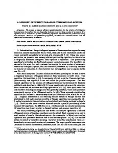
2. PROPOSAL OF THE ARCHITECTURE 2.1 Possible architectures used for DSP in FPGA In many applications simple pipelined data-path architecture may be used for DSP algorithms. This approach is well supported with tools like Xilinx System Generator6 or Altera DSP Builder.7 Our team has used this approach when implementing a simple, introductory version of RF control system for an accelerator cavity.8 A part of this system performing so called ”Matrix Rotation”, implemented in Xilinx System Generator is shown in the Fig.1. However the above method is not suitable for more complex problems, in which the same arithmetical block should be used for different purposes in consecutive steps of the algorithm. In this approach, we need some processing units controlled by the state machines, which control the data flow between those units and storage
1 I_In
a (ab) xlmult b z−2
Xxlshift >> 18 Shift
Mult 2 Q_In
a (ab) xlmult b z−2
Xxlshift >> 18
a xladdsub a−b b z−1
xlshift X >> 0 Shift4
1 I_Out
AddSub
Shift1
Mult1
a (ab) xlmult b z−2
Xxlshift >> 18 Shift2
Mult2
3 cosPhi_K
a a+b xladdsub b z−1 a
4 sinPhi_K
xlmult (ab) b z−2
Xxlshift >> 18
xlshift X >> 0 Shift5
2 Q_Out
AddSub1
Shift3
Mult3
Figure 1. Part of the RF control system, performing the ”Matrix Rotation” operation, implemented in pipelined datapath architecture using the Xilinx System Generator. After every clock pulse the new result is presented on the output, however the processing latency is higher, and depend on the number of pipeline registers built into the pipeline (Figure cited from Ref.8).
Processing Unit
Data Register
Processing Unit
Data Register
[...]
[...]
Processing Unit
Data Register
Data flow controll Data processing commands
Figure 2. The architecture for implementation of DSP algorithms in FPGA based on state machine, controlling processing units and the data flow.
Data Memory
Data Memory Bus
Processing Unit
Processing Unit
Processing Unit
Code Memory Bus Code Memory
Figure 3. The flexible architecture for DSP in FPGA with multiple processing units sharing the same code memory and data memory.
elements as shown in the Fig.2. An example of such approach was an accelerator’s cavity simulator developed by our team.9 This system had to solve differential state equations, which required a sequential algorithm. In this system registers have been used to store the numerical data between calculations. This assured easy simultaneous access to multiple arguments needed by the processing units, but resulted in high routing resources consumption. This consumption was reduced by hard-coding of the algorithm which allowed the synthesis tools to remove in the optimization phase all connections not used by the particular algorithm. Such optimization is not possible in fully programmable systems, so another architecture is needed. Use of registers (synthesized from flip-flops) is also not acceptable if more storage space is needed. If we need more storage, we have to use the memory for processed data. Use of memory to store the code controlling the processing units instead of state machine with hard-coded algorithm may be also advantageous, as it provides programmability and allows to build very flexible system. However in such approach we simply imitate the structure of the multicore DSP processor,10 so it is unlikely to obtain better results with a programmable FPGA chip, than with the dedicated, carefully tuned DSP processor chip. Additionally sharing of memory between multiple units requires a complex bus arbitration which would dramatically impair the performance of that system. The simplest way to improve this architecture is to provide a separate code memory for each processing unit. The similar separation of the data memories is however not possible if we want to use the data memory to exchange data between processing units. Therefore the shared data memory bus is a real bottleneck in this architecture. To overcome this limitation another mechanism is needed providing reasonable storage capacity, and allowing efficient exchange of information - namely the dual port memory.
2.2 Use of dual port memory for DSP in FPGA Modern FPGA chips provide multiple dual port RAM memory blocks (DPRAM). High end chips may contain even more than 2000 DPRAM blocks with capacity of 20 kbits (Altera Stratix V11 ) or more than 2100 DPRAM blocks with capacity of 18 kbits (Xilinx Virtex-612 ). Even low end devices from cheap families offer 46 blocks with capacity of 9 kbits (Altera Cyclone III EP3C513 ) or 12 blocks with capacity of 18 kbits (Xilinx Spartan 6 XC6SLX414 ). The DPRAM allows almost independent access from two buses (Figure 4). The only conflicting situation arises when both ports are trying to write new contents to the same address. In some implementations also simultaneous read and write accesses to the same address should be avoided. Even with the mentioned limitations the DPRAM block may be a very efficient way to exchange information between two systems.15 They are often used to implement FIFOs allowing to transmit data between different clock domains. In the proposed architecture DPRAM blocks are used to create the data storage shared by two neighboring processing units. In this way we avoid building a global shared data memory and bypass problems associated with necessity Further author information: (Send correspondence to W.M.Z.) W.M.Z.: E-mail:
[email protected], Telephone: +48 22 234 7717
Memory Port A
Data output A Address A Write Enable A
Data Output B
Dual Port RAM Memory
Address B Write Enable B Clock B
Clock A
Memory Port B
Data Input B
Data Input A
Figure 4. The flexible architecture for DSP in FPGA with multiple processing units sharing the same code memory and data memory.
Data DP RAM
[...]
Synchronization
Data DP RAM
Synchronization
DPS
Synchronization
To other Processing Units
Data DP RAM
Code DP RAM
DPR
Control registers access
Processing Unit
Data DP RAM
Single processing unit
Programming interface
Figure 5. Basic cell in the DSP in FPGA architecture based on a DPRAM blocks used for exchange of information.
of access arbitration. Only very simple handshake is needed to avoid the mentioned problem with simultaneous write access, and this handshake may be easily integrated with the synchronization interface which is anyway needed in a system consisting of multiple processing units operating in parallel. This synchronization interface contains a few unidirectional lines in both directions. Each unit may set its synchronization outputs to notify its neighbor about events associated with data processing, and may check its synchronization inputs to receive notifications from its neighbor. One DPRAM memory is used to connect each processing unit with the “programming interface” used to load programs performed by processing units, and data or coefficients used in calculations. To perform these tasks, this memory is divided into two areas - the first one used to store the code, and the second - allocated for data transmitted to the DSP system by the programming interface and received from the DSP system by the programming interface. Of course the main stream of data in the real DSP system should be transmitted through faster interfaces. To achieve that some processing units should be integrated with the high speed I/O interfaces like RocketIO16 or GXB17 The “programming interface” provides also access to internal registers in processing units, needed to control each unit and to check its status. The proposed basic cell of the DSP system built in the FPGA is shown in the Fig.5
2.3 Interconnections between processing units Another problem to be solved is the topology of interconnections between the processing units. In the simplest approach, shown in the Fig.6 the processing units are organized in a chain. Each processing unit has three memory interfaces - one connected to the programming interface (through the CODE/DATA DPRAM), and two connected to its neighbors. To allow quicker propagation of information through the chain, the 4th memory
DP RAM + Reg. acc.
DP RAM + Reg. acc.
[...]
DP RAM + Reg. acc.
Processing Unit
DP RAM + Synchro
Processing Unit
DP RAM + Synchro
Processing Unit
DP RAM + Synchro
Processing Unit
DP RAM + Synchro
DP RAM + Synchro
DP RAM + Reg. acc.
Programming interface
Figure 6. Simple layout of interconnections between processing units - a single chain. DPS
connection with the 1st unit (4+3) mod 6=1
connection with the 4th unit (1-3) mod 6=4
DPS
DPS PU0 DPR
DPS
PU1
DPS
DPR
PU2 DPR
DPS
PU3
DPS
DPR
PU4 DPR
DPS
PU5
DPS
DPR
Programming interface Figure 7. Layout of interconnections between the processing units with ”bypass connections”. PU: processing unit, DPS: DPRAM and synchronization interface, DPR: DPRAM and register access interface
interface has been added, which allows to create ”bypass connections”, as shown in the Fig.7. With four memory interfaces each processing unit may in a single clock cycle - read the instruction from the code memory, read two arguments from 2 shared data DPRAMs and write the result of the previous operation into the 3rd shared data DPRAM. The above interconnection scheme may be easily described with the following rules: • If N is the number of processing units, and N is an even integer number not less than 6 • If the processing units are numbered from 0 to N − 1 • The k-th unit should be connected via the bypass connection to the j-th unit, where j is calculated as follows: – for even k: j = (k + 3)modN – for odd k: k = (k − 3)modN The above description allows to write the synthesizable VHDL code with parametrized number of processing units, and to easily experiment with systems containing different amount of processing units.
3. IMPLEMENTATION The proposed architecture has been implemented in the VHDL language. For first ”proof of the concept” implementation very simple processing units with limited functionalities have been used. The instructions were 32-bits long and worked with the data treated as 32-bit fixed point integers. Only basic operations like addition, subtraction, multiplication, shifting, and logical operators have been implemented. To allow implementation of more complex algorithms, also the loops, comparisons, jumps and conditional branches have been added. Each processing unit was also equipped with a small 16-level stack, which allowed to implement procedures.
Table 1. Results of synthesis of DSP system with 6 processing units in Virtex-4 xc4vlx15-12 chip.
Device Utilization Summary Number of BUFGs 2 out of 32
6%
Number of DSP48s
24 out of 32
75%
Number of External IOBs
68 out of 240
28%
Number of LOCed IOBs
0 out of 68
0%
Number of RAMB16s
48 out of 48
100%
Number of Slices
6142 out of 6144
99%
Number of SLICEMs 0 out of 3072 Speed parameters Maximum clock frequency
0% 66.6MHz
Table 2. Results of synthesis of DSP system with 6 processing units in Virtex-4 xc4vlx25-12 chip.
Device Utilization Summary Number of BUFGs 2 out of 32
6%
Number of DSP48s
24 out of 48
50%
Number of External IOBs
68 out of 240
28%
Number of LOCed IOBs
0 out of 68
0%
Number of RAMB16s
72 out of 72
100%
Number of Slices
6743 out of 10752
62%
Number of SLICEMs 0 out of 5376 Speed parameters Maximum clock frequency
0% 68.49MHz
To allow synchronization between different processing units, simple instructions like setting, clearing and testing of individual bits in the synchronization interface have been provided. Each processing unit was equipped with registers allowing to control and monitor its state. Also some global registers have been added allowing to detect whether any processing unit signals the processing error, and to start or stop all processing units simultaneously.
4. TESTS AND RESULTS The proposed architecture has been tested in a dedicated hardware-software co-simulation environment using the GHDL simulator and Python language. This environment allowed to emulate the VME-like programming interface for the simulated DSP system. The tests have proved correct operation of the simulated DSP system. The proposed architecture has been also synthesized with Xilinx ISE toolset for different chips from Virtex-4 family, however no tests in real hardware have been performed yet. To check scalability of the proposed solution two versions of the DSP system have been synthesized: the first one with 6 processing units, and the second one with 12 processing units. Each version was synthesized for the smallest chip which was able to contain the system, and then for the next, bigger chip. The synthesis was successful and its results are shown in the Tables 1, 2, 3 and 4. Even the smallest members of Virtex-4 family provide sufficient resources to implement the DSP system with 6 processing units. The achievable clock frequency is equal to c.a. 66MHz, however it should be possible to improve this by adding pipeline registers in the processing units. Doubling of numbers of processing units does not lower significantly the maximum clock frequencies, if we use a chip with sufficient resources (compare tables
Table 3. Results of synthesis of DSP system with 12 processing units in Virtex-4 xc4vlx25-12 chip.
Device Utilization Summary Number of BUFGs 2 out of 32
6%
Number of DSP48s
48 out of 48
50%
Number of External IOBs
68 out of 240
28%
Number of LOCed IOBs
0 out of 68
0%
Number of RAMB16s
72 out of 72
100%
Number of Slices
10750 out of 10752
99%
Number of SLICEMs 0 out of 5376 Speed parameters Maximum clock frequency
0% 55.47MHz
Table 4. Results of synthesis of DSP system with 12 processing units in Virtex-4 xc4vlx40-12 chip.
Device Utilization Summary Number of BUFGs 2 out of 32
6%
Number of DSP48s
48 out of 64
75%
Number of External IOBs
68 out of 448
15%
Number of LOCed IOBs
0 out of 68
0%
Number of RAMB16s
96 out of 96
100%
Number of Slices
13414 out of 18432
72%
Number of SLICEMs 0 out of 9216 Speed parameters Maximum clock frequency
0% 66.68MHz
2 and 4). Use of too small chip may result in significant drop of maximum clock frequency due to inefficient internal routing of signals (compare tables 3 and 4). Comparison of number of slices in tables 2 and 4 suggests that the logical resources consumption is almost proportional to the number of processing units. Obtained results allow to assume, that the proposed architecture is reasonably scalable.
5. FURTHER WORK 5.1 Non-uniform architectures The tested ”proof of the concept” architecture was uniform - all processing units provided the same functionality. In the real operating system however some processing units may offer extended functionality - e.g. performing of more complex operations like division or calculation of square root. The interesting question will be how integrate those “extended processing units” with rest of the system. In this paper no problems associated with the input and output have been discussed. In the real system however some processing units should be equipped with additional functionality to service a serial or parallel I/O interface.
5.2 Programming tools The proposed architecture offers good computational power at reasonable costs, but it may be difficult to programming. Development of code for state machine controlled parallel architecture described in Ref.9 proved to be possible but time consuming and error prone. The proposed architecture may be even more difficult to program, especially if we consider non-uniform versions proposed in the previous subsection, or different latencies
associated with some more complex operations. The distribution of data buffers and coefficients between different available memories may also significantly affect the processing speed. Therefore dedicated tools are needed to optimally organize data distribution and to automatically generate code for processing units. The first attempts to prepare such a tool are described in Ref.18
6. CONCLUSIONS The architecture described in this document provides a scalable method for implementation of highly parallel DSP algorithms in the FPGA chip. Use of dual port memory (DPRAM) allows to efficiently transfer data between independently operating processing units minimizing overhead related to access arbitration. The resources consumption is almost linearly dependent on the number of processing units, which assures good scalability. The scalability may be affected however by the maximum size of the DPRAM blocks used to connect processing units. The performance of some algorithms may be significantly lowered, when the data structures (vectors, matrices) do not fit into single DPRAM block. The significant disadvantage of the proposed architecture may also be a difficulty to transform the standard DSP algorithm into the highly parallel form, well suited for execution on the platform with multiple small data memories and multiple processing units. The reliable generation of code may require dedicated programming tools.
REFERENCES [1] “Digital Signal Processing (DSP) Blocks in Stratix Devices.” . [2] “XtremeDSP 48 slice.” . [3] “OpenCores.” . [4] “Open source FPGA floating point library.” . [5] “IEEE Standard VHDL Language Reference Manual,” IEEE Std 1076-2008 (Revision of IEEE Std 10762002) , c1 –626 (jan. 2009). [6] “System Generator for DSP Reference Guide.” . [7] “DSP Builder.” . [8] Zabolotny, W. M., Pozniak, K. T., Romaniuk, R. S., Czarski, T., Kudla, I. M., Kierzkowski, K., Jezynski, T., Burghardt, A., and Simrock, S., “Design and simulation of fpga implementation of a rf control system for the tesla test facility,” Photonics Applications in Astronomy, Communications, Industry, and High-Energy Physics Experiments 5125(1), 223–230, SPIE (2003). [9] Zabolotny, W. M., Bunkowski, K., Czarski, T., Jezynski, T., Pozniak, K. T., Rutkowski, P. Z., Simrock, S., and Romaniuk, R. S., “Fpga-based cavity simulator for tesla test facility,” Photonics Applications in Astronomy, Communications, Industry, and High-Energy Physics Experiments II 5484(1), 139–147, SPIE (2004). [10] “TMS320C6474 multicore digital signal processor.” . [11] “Stratix V FPGAs: Built for bandwidth.” . [12] “Virtex-6 FPGA family overview.” . [13] “Cyclone III FPGA family overview.” . [14] “Spartan-6 family overview.” . [15] LaRue, J. and Tseng, D., “Dual-port FPGA memory blocks: the ultimate system interconnect solution?.” . [16] “Virtex-5 FPGA RocketIO GTP transceiver user guide.” . [17] “Stratix GX transceiver user guide.” . [18] Berdychowski, P. P. and Zabolotny, W. M., “C to VHDL compiler.” This Volume.