Abstract. Iris is touch-less automated real-time biometric system for user authentication. ...... The sphincter muscle lies around the very edge of the pupil. In bright.
Minoufiya University Faculty of Electronic Engineering- Menouf Department of Computer Science and Engineering
Field Programmable Gate Array (FPGA) - Based Implementation of Iris Recognition Systems A Thesis Submitted for the Degree of M. Sc. in Electronic Engineering Computer Science and Engineering Department of Computer Science and Engineering
By
Eng. Ramadan Mohamed Abdel-Azim Gadel-Haq B. Sc. in Electronic Engineering Computer Science and Engineering Department Faculty of Electronic Engineering, Minoufiya University. 2005
Supervised By
Prof. Dr. Nawal Ahmed El-Fishawy Head of Department of Computer Science and Engineering Faculty of Electronic Engineering, Minoufiya University.
2012
A--+!j.f , &...*rqt ! M inoutiya University
Faculty of Fllectrouic Engineering- Mer-rouf
I)eparlrnent of Computer Science and Engineering
Field Programmable Gate Array (FPGA) - Based Implementation of lris Recognition Systems A Thesis Submitted lor the Degree of M. Sc. in Electronic Engineering Computer Science and E,ngineering Department of Computer Science and E,ngineering
Ilv Eng. Ramadan Mohamed Abdel- Azim Gadel-Haq B. Sc. in Electronic Iingineering Computer Science and Engineering Department Faculty of Electronic Engineering, Minoufiya University. 2005
Supervised By
Prof. Dr. Nawal Ahmed El-Fishawy
(
/d4
)
Head of Department of Cornputer Science and Engineering
Faculty of Electronic Engineering.
Minoufiya lJniversity
20t2
Minoufiya University Faculty of Electronic Enginecring- Menouf Department of Comptrter Science and Engineering
Field Programmable Gate Array (FPGA) - Based Implementation of Iris Recognition Systems A Thesis Submitted for the Degree of M. Sc. in Electronic Engineering Computer Science and Engineering Department of Computer Science and Engineering By
Eng. Ramadan Mohamed Abdel-Azim Gadel-Haq B. Sc. in Electronic Engineering Computer Science and Engineering Department Faculty of Illectronic Engineering, Minoufiya lJniversity. 200s
Approved by
Pror'
"' iffftYt'A
ra
rat AIi
Ilead of the Department oly'/^prrters engineering and systems Faculty of Engin6ering. Mansoura lJniversity.
Prof. Dr. NawalAhmed El-Fishawy
(
P-rA Cori'pt,,hcience'ona )
Heacl of the Departn-rent of
engineering Faculty of Electronic Engincering, Minoufiya University.
Dr. Fathi El-Sayed Abd EI-Samie
(frfl)
Department ol Elcctfonics ancl Lrlectrical (lornmunic:at ions Faculty of Electronic Engineering, Minoutiya University.
2012
Acknowledgments
My great gratitude is directed to Allah for helping me to finish this thesis with satisfactory results. I would like to express my deep gratitude and thanks to Dr. Mohamed Abdel-Azim for his invaluable supervision, encouragement, great cooperation and constructive comments. Also special thanks to my supervisor Prof. Nawal El-Fishawy For her efforts in this study and support she gave me. Thanks to all staff in my department of Computer Science and Engineering in my faculty. My sincere and grateful thanks to my professors in the faculty, who taught me many things and were very friendly with me. Also, I express great thanks to my family members for their encourages.
i
Abstract
Abstract Iris is touch-less automated real-time biometric system for user authentication. Pattern recognition approaches suffer from high cost, long development times, and computationally intensive. General Purpose Systems are low speed and not portable; FPGA-based system prototype implemented by using VHDL language. Iris recognition system is, implemented in software. To overcome the problems of obtaining a real-time decision of the human iris in an accurate, robust, low complexity, reliable, and fast technique. Threshold concepts are used to segment the pupil. Canny edge detector and Circular Hough Transform are used to localize the iris region. Rubber Sheet Model is used as an unwrapping and normalization algorithm. Histogram equalization technique is used to enhance the normalized iris image contrast. Iris features are extracted and encoded using 1D log-Gabor transform and the DCT respectively. Finally, the template matching is performed using the Hamming distance operator. Experimental tests on the CASIA (version 1) database achieved 98.94708% of recognition accuracy using 1D Log-Gabor with Equal Error Rate (EER) equal to 0.869%. The FAR and FRR are 0% and 1.052923% respectively. In contrast, 93.07287% of accuracy using DCT with EER equal to 4.485%. The FAR and FRR are 0.886672% and 6.040454%, respectively. The proposed approach (FDCT-based feature extraction and Hamming Distance stages) are implemented and synthesized using Xillinx FPGA chip (XC3S1200E-4fg320), occupying 1% of chip CLBs. It achieved 58.88 µs to process and takes a decision compared with current software implemented taking 1.926794 s. A 1D log-Gabor iris recognition system is more accurate and secure. However, DCT-based one is more reliable, having a low computational cost and a good interclass separation in a minimum time. The hardware implementation is small and fast enough. ii
Table of Contents
Contents Acknowledgments…………………………………………………………………..
i
Abstract……………………………………………………………………………..
ii
Contents……………………………………………………………………………..
iii
List of Tables………………………………………………………………………..
vi
List of Figures……………………………………………………………………….
vii
List of Abbreviations……………………………………………………………….
ix
Chapter-1: Introduction…………………………………………………………… 1.1 Introduction………………………………………………… ………………
1 1 4 5 8 9
1.1.1 Problem Statement .…………………………………………………………. 1.1.2 Current Research……………………………………………………………..
1.2 Work Aims………………………………………………………………….. 1.3 Work Organization………………………………………………………….. Chapter-2: Biometric Security Systems…………………………………………... 2.1 Introduction…………………………………………………………………. 2.2 Biometric Definition and Terminology……………………………………... 2.3 Biometric History…………………………………………………………… 2.4 Biometric Characteristic Requirements…………………………………….. 2.5 Biometric Systems…………………………………………………………..
2.7 Performance of Biometric Systems………………………………………….
12 12 13 15 15 17 17 19 19 24 26
Chapter-3: Human Vision System………………………………………………… 3.1 Eye Anatomy………………………………………………………………... 3.2 Iris Recognition Systems……………………………………………………. 3.3 Medical Conditions Affecting Iris Pattern…………………………………. 3.4 Iris System Challenges……………………………………………………… 3.5 Advantages of Iris Systems…………………………………………………. 3.6 Disadvantages of Iris System…………...…………………………………...
29 29 32 33 34 35 35
Chapter-4: Iris Database and Dataset……………………………………………. 4.1 Iris Image Acquisitions……………………………………………………... 4.2 Brief Descriptions of Some Datasets………………………………………..
36 36 36 37 38 39 39
2.5.1 Modes of Operation………………………………………………………….
2.6 A Brief Overview of Commonly Used Biometrics…………………………. 2.6.1 Physiological Characteristic Biometrics…………………………………….. 2.6.2 Behavioral Characteristic Biometrics………………………………………..
4.2.1 Chinese Academy of Sciences - Institute of Automation (CASIA 1)……….. 4.2.2 Iris Challenge Evaluation (ICE)……………………………………………... 4.2.3 Lions Eye Institute…………………………………………………………... 4.2.4 Multimedia University (MMU 1 and MMU 2)……………………………… iii
Table of Contents
4.2.5 University of Bath Iris Image Database (UBIRIS)…………………………..
4.3 Dataset Used………………………………………………………………… Chapter-5: Image Preprocessing Algorithm……………………………………... 5.1 Proposed Iris Recognition System………………………………………….. 5.2 Iris Localization…………………………………………………………….. 5.2.1 Detecting the Pupil Boundary……………………………………………… 5.2.2 Detecting the Iris Boundary………………………………………………… 5.2.2.1 John Daugman Approach………………………………………………………. 5.2.2.2 Richard Wildes Approach……………………………………………………… 5.2.2.3 Proposed Algorithm for Iris Segmentation……………………………………..
5.3 Iris Normalization and Unwrapping………………………………………… Chapter-6: Iris Code Generation and Matching……………………………….… 6.1 Iris Image Enhancement …………………………………………………… 6.2 Iris Feature Extraction…………………………………………………….… 6.2.1 1D Log-Gabor Wavelet…………………………………………………...…
6.2.2 The Discrete Cosine Transform (DCT)……………………………….. 6.3 Template Matching…………………………………………………………. 6.4 Experimental Results……………………………………………………….. Chapter-7: System Hardware Implementation……………………………….…. 7.1 Introduction……………………………………………………………….… 7.1.1 The Evolution of Programmable Devices………………………………......
7.2 FPGA Overview……………………………………………………………. 7.2.1 Architecture Alternatives…………………………………………………... 7.2.1.1 FPGAs vs. GPPs……………………………………………………………. 7.2.1.2 FPGA vs. ASIC…………………………………………………………….. 7.2.1.3 FPGAs vs. DSPs…………………………………………………………….
7.2.2 Advantages of Using FPGA……………………………………………….. 7.2.3 FPGA Structure……………………………………………………………. 7.2.3.1 FPGA Programming Technologies…………………………………………… 7.2.3.2 FPGA Interconnect Architecture ………………………………………….. 7.2.3.3 General FPGA architecture …………………………………………………… 7.2.3.4 Logic Block Trade-Offs with Area and Speed ………………………………..
7.2.4 Case Study of Xilinx FPGA Architectures ………………………………
7.3 Overview of HDL and Implementation Tools…………………………….. 7.3.1 Xilinx Integrated Software Environment (ISE) …………………………... 7.3.2 VHDL vs. Verilog HDL…………………………………………………… 7.3.3 Xilinx FPGA Design Flow and Software Tools…………………………… 7.3.4 HDL Coder………………………………………………………………....
7.4 FPGA Applications………………………………………………………… 7.5 Image Processing Overall System…………………………………………. 7.6 System Emulation………………………………………………………….. 7.6.1 HDL Code…………………………………………………………………. 7.6.2 System Hardware Simulation Results……………………………………… iv
40 41 42 42 43 44 44 45 46 48 49 54 54 55 65 59 61 63 74 74 76 80 81 83 84 86 87 89 89 93 94 98 100 102 104 105 106 111 113 114 120 120 121
Table of Contents
7.7 Implementation and Download…………………………………………… 7.8 Design Issues……………………………………………………………… 7.8.1 Issues in Hardware Implementation……………………………………….
124 126 127
Chapter-8: Conclusions and Future Work…………………………………….. 8.1 Conclusion………………………………………………………………… 8.2 Suggestions for Future Work………………………………………………
130 130 131
References …………………………………………………………………………
133
v
List of Tables
List of Tables Table No.
Page No.
Table Caption
Table 2.1
Comparison of various biometric technologies.
25
Table 4.1
Mostly used iris databases.
37
Table 6.1
The average HD results of 1D Log-Gabor based template matching.
67
Table 6.2
The average HD results of DCT based template matching.
67
Table 6.3.
Results of verification test for 1D Log- Gabor filter.
69
Table 6.4
Results of verification test for DCT method.
69
Table.7.1
The main comparison between CPLD and FPGA.
80
Table 7.2
The main differences technologies.
92
Table 7.3
Some of the commercially available FPGAs.
92
Table 7.4
Popular FDCT Algorithms Computation when N=8.
118
Table 7.5
XC3S1200E FPGA device utilization summary.
125
between
vi
FPGA
programming
List of Figures
List of Figures Figure No.
Page No. 14
Figure Caption
Figure (2.1) Examples of biometric characteristics Figure (2.2) A components of biometric system
18
Figure (2.3) Biometric system error rates
28
Figure (2.4) Receiver operating characteristic (ROC)
28
Figure (3.1) Anatomy of the human eye
29
Figure (3.2) The human iris front-on view
30
Figure (3.3) Anatomy of the iris visible in an optical image
31
Figure (4.1) Example iris images in CASIA-IrisV1
38
Figure (4.2) Example iris images in ICE-2006
38
Figure (4.3) Example iris images in MMU 1
39
Figure (4.4) Example iris images in UPIRIS
40
Figure (5.1) Stages of iris recognition algorithm
42
Figure (5.2) Block diagram of iris recognition system.
43
Figure (5.3) Pupil boundary detection steps
44
Figure (5.4) Iris localization steps:
49
Figure (5.5) Result of the proposed segmentation algorithm
49
Figure (5.6) Implementation of unwrapping step.
52
Figure (5.7) Unwrapping and normalization
52
Figure (5.8)
A sample results implementation
of
unwrapping
and
normalization
53
Figure (6.1) Enhanced normalized iris template with histogram
55
Figure (6.2) 1D-Log Gabor filter and encoding idea
59
Figure (6.3) Iris code generation
59
Figure (6.4) Encoded iris texture after DCT transform
61
Figure (6.5)
False Accept and False Reject Rates for two distributions with a separation Hamming distance of 0.35
63
Figure (6.6)
Probability distribution curves for matching and nearest non matching Hamming distances of 1D Log-Gabor method.
68
Figure (6.7)
Probability distribution curves for matching and nearest non matching Hamming distances of DCT method.
68
vii
List of Figures
Figure (6.8)
Receiver Operating Characteristic (ROC) curve of 1D LogGabor method
70
Figure (6.9)
FAR and FRR versus Hamming Distances of 1D Log-Gabor approach.
70
Figure (6.10)
Receiver Operating Characteristic (ROC) curve of DCT method.
71
Figure (6.11) FAR and FRR versus Hamming distances for DCT approach.
71
Figure (6.12) ROC of both 1D Log-Gabor and DCT approaches.
72
Figure (6.13)
FRR versus Hamming distances of both 1D Log-Gabor and DCT approaches.
Figure (6.14) Iris recognition system (GUI) interface.
72 73
Figure (7.1) internal architecture of the simplified version of FPGA
95
Figure (7.2) General FPGA fabric.
95
Figure (7.3) General FPGA blocks and connections (zoomed view).
95
Figure (7.4)
Xilinx (XC4000E) CLB.
98
Figure (7.5) PSM and interconnection lines. (XC4000E Interconnections). Figure (7.6) Levels of abstraction.
104
Figure (7.7) ISE 12.1 GUI main window
105
Figure (7.8)
FPGA design flow.
98
110
Figure (7.9) The overall proposed system.
116
Figure (7.10) 1D-DCT model by using adders and multiply.
119
Figure (7.11) The proposed system under Simulink simulation tool
121
Figure (7.12) GUI of Modelsim simulator (main window).
122
Figure (7.13) Simulation of the iris hardware architecture with fixed point using ModelSim. Figure (7.14) Schematic (RTL) view of the synthesized code.
123
viii
124
List of Abbreviations
List of Abbreviations ROM
Read Only Memory
FPGA
Field Programmable Gate Array
PCI
Peripheral Component Interconnect bus
ASIC
Application Specific Integrated Circuit
DSP
Digital Signal Processing
CHT
Circular Hough transform
DCT
Discrete Cosine Transform
HD
Hamming Distance
IP
Intellectual Property
LED
Light-Emitting Diode
LCD
Liquid Crystal Display
FDCT
Fast Discrete Cosine Transform
ATM
Automatic Teller Machines
FNMR
False Non-Match Rate
FMR
False Match Rate
PIN
Personal Identification Number
ROC
Receiver Operating Characteristic
FTC
Failure to Capture
FTE
Failure to Enroll
NIR
Near Infrared illumination
CASIA
Chinese Academy of Sciences Institute of Automation
ICE
Iris Challenge Evaluations
LEI
Lions Eye Institute
MMU
Multimedia University
UBIRIS University of Bath Iris Image Database CHT
Circular Hough Transform
PLD
Programmable Logic Devices
GPP
general purpose processors
PLA
Programmable Logic Arrays ix
List of Abbreviations
PAL
Programmable Array Logic
PROM
Programmable Read Only Memory
CPLD
Complex Programmable Logic Devices
LUT
Look-Up Table
HDL
Hardware Description Language
SRAM
Static Random Access Memory
CLB
Configurable Logic Blocks
PSM
Programmable Switch Matrix
PSoC
Programmable System-on-a-Chip
EDA
Electronic design automation
ISE
Xilinx Integrated Software Environment
RTL
Register transfer level
VHDL
VHSIC Hardware Description Language
NGD
Native generic database
UCF
User constraints file
MAC
Multiply-Accumulators
x
Chapter 1
Introduction
Chapter 1
Introduction 1.1 Introduction Security of computer and financial systems plays a crucial role nowadays. These systems require remembering many passwords that may be forgotten or even stolen. Thus biometrical systems, based on physiological or behavioral characteristics of a person, are taken into consideration for a growing number of applications. These characteristics are unique for each person, and are more tightly bound to a person than a token object or a secret, which can be lost or transferred. Therefore, touch-less automated real-time biometric systems for user authentication, such as iris recognition, became a very attractive solution. It has been successfully deployed; in several largescale public applications, increasing reliability for users and reducing identity fraud. This method of identification depends on relatively unchangeable features and thus it is more accurately defined; as authentication [1, 2]. Within the last decade, governments and organizations around the world have invested heavily in biometric authentication for increased security at critical access points, not only to determine who accesses a system and/or service, but also to determine which privileges should be provided to each user. For achieving such identification, biometrics technology is emerging as a technology that provides a high level of security, as well as being convenient and comfortable for the citizen [3]. For example, the United Arab Emirates employs biometric systems to regulate the people traffic across their borders. Subsequently, several biometrics systems have attracted much attention, such as facial recognition and iris recognition [4]. Iris recognition is more abstract.
-1-
Chapter 1
Introduction
Most biometric systems are based on computer solutions. Many computer systems have operating systems that run in the background along with many other concurrent processes or programs that can slow the generalpurpose system down [5]. Furthermore, general-purpose systems are not especially mobile (with the exception of very lightweight laptop computers) and thus may not serve every venue where iris recognition systems could be deployed. Thus, a hardware implementation of an iris recognition system is especially interesting as it could be exceptionally faster than its generalpurpose counterpart could also, being small enough to be part of a digital camera or camera phone. However, hardware/software co-design is a suitable solution, widely used for developing specific and high computational cost devices. This provides a means of embedded systems [3, 6]. An embedded system can be defined as a generalized term for many systems, which satisfy all (or at least most) of the following requirements [5]: (i) Always designed for a specific purpose; (ii) Typically small in dimensions, Due to their performance restrictions; (iii) The cost of these systems is lower than that of a general purpose machine; (iv) These systems usually make use of Read Only Memory (ROM) memories to store their programs and not hard disks or any other big storage systems; (v) Due to the application, most of these systems work under real time constraints, such applications range from time sensitive to time critical; (vi) There is a large variety of applications for these types of systems; (vii) They may also form a part of a larger system, and (viii) In an embedded system, one or several co-processors are developed according to the systems requirements. One of the embedded system examples is the field programmable gate arrays (FPGAs). It has evolved from simple “glue logic” circuits into the central components of reconfigurable computing systems [7].
In general,
FPGAs consist of grids of reprogrammable logic blocks, connected by meshes of reprogrammable wires. Reconfigurable computing systems combine one or -2-
Chapter 1
Introduction
more FPGAs with local memories and Peripheral Component Interconnect (PCI) bus connections to create reconfigurable co-processors [8]. FPGA architecture has a dramatic effect on the quality of the final device speed performance, area efficiency, and power consumption. The reconfigurability property makes them ideal prototyping tools for hardware designers [9]. Prototypes can help unveiling design bugs, which might be hidden in the simulation stage because they allow exploring the behavior of a "real" product. In particular, FPGA prototypes are suited to explore the behavior of hardware components. FPGA prototypes allow designers to estimate parameters, which are typical for design portions to be implemented in an Application Specific Integrated Circuit (ASIC) or FPGA, like real time algorithms with extensive, repetitive multiplications. One such parameter is the area consumption of the component, which is strongly influenced, besides design complexity, by the utilization of FPGA specific hard macros, like multipliers, block RAMs or DSP-slices. Even timing issues, as long critical paths, can be analyzed, because they will not be much different in the final product. Another reason for building a prototype is to convince potential customers of the capabilities of the product, which might be far from completion. However, a drawback of prototypes is that for nowadays-high complexity systems their implementation is costly and time consuming [10]. Advances in algorithms and in the processing power of embedded hardware systems allow for the beginnings of real-time human-like vision capabilities within the confines of relatively restricted domains, despite the high computational complexity of these algorithms [11]. This chapter is organized as follows: Section 1.1.1 presents thesis problem statement. Then, section 1.1.2 discuses the motivations for this work. Our work goals are identified in Section 1.2. Finally, Section 1.3 describes the thesis organization. -3-
Chapter 1
Introduction
1.1.1 Problem Statement The embedded devices in biometrics have gained increasing attention due to the demand for reliable and cost-effective personal identification systems [12]. Building such robust, more accurate, non-intrusive to humans, and fast real-time iris recognition system, by using only software has some insufficiency. Therefore, the current trend is hardware/software co-design.
Contemporary state of the art in real-time image pattern recognition is a challenging task, which involves image processing, feature extraction and pattern classification [1, 7]. These approaches suffer from various disadvantages, such as high cost and long development times. In addition, these algorithms have high consumption of computational power (requires intensive computations), and this causes high power consumption. Software-based implementation of a pattern recognition system relies on a low speed computer and is not suitable for use in the environments where high portability is required [8]. Consequently, some applications are sensitive to battery life, heat dissipation, etc.; recent advances in fabrication technology allow the manufacturing of high density and high performance FPGAs capable of performing many complex computations in parallel while hosted by conventional computer hardware [13, 14]. Once, the hardware platform has a low-power processor without any hardware implemented floating-point arithmetic. To execute the biometric systems in real-time, some tasks of the biometric algorithms that demand a high computational power can be implemented into FPGA. These tasks can be dynamically synthesized on the FPGA to speed up the biometric algorithms. If Application Specific Integrated Circuits (ASICs) is the design target embedded devices due to their performance speeds, FPGAs offer a good flexibility in design and prototyping tools [7, 12]. -4-
Chapter 1
Introduction
Significant speed-up in computation time can be achieved by assigning complex computation intensive tasks to hardware and by exploiting the parallelism in algorithms. FPGA is a platform of the choice for hardware realization of computation-intensive applications [15]. The advantage of using FPGA is that it can be reprogrammed at a logic gate level for each different specific application. One of the main objectives is to minimize the complexity of operations as much as possible while maintaining low delays and high speed throughputs [16, 17].
1.1.2 Current Research The properties of the human eye iris are stable throughout the life of an individual, and therefore the iris a suitable biometric modality. The biometric properties of every iris are unique [18]. The iris identification using analysis of the iris texture has attracted a lot of attention, and researchers have presented a variety of approaches. Daugman [19] has presented the most promising 2-D Gabor filter-based approach for the iris identification system. He used an Integro-differential operator to find the pupillary boundary and the limbus boundary as circles. Then, Rubber Sheet Model is used to normalize the iris. Hamming Distance (HD) was his classifier operator to match the templates. Daugman's overall system has an excellent performance and accuracy. It uses a binary representation for iris code. Moreover, this speeds the matching through HD. In addition, ease handling of rotation of iris. In addition, interpretation of matching as a result of statistical test of independence. On the other hand the system is Iterative and computationally expensive. In addition, evaluation of iris image quality reduces to the estimation of a single or a pair of factors such as defocus blur, motion blur, and occlusion.
-5-
Chapter 1
Introduction
Boles [20] has detailed fine-to-coarse approximations at different resolution levels that are based on zero-crossing representation from the wavelet transform decomposition. Wildes et al. [21] have focused on efficient implementation of gradient-based iris segmentation using Laplacian of Gaussian filters (Laplacian pyramid). He isolated the iris by using edge detector and Hough Transform. By using image registration technique the images aligned well to be compared and matched by normalized correlation classifier. It Accounts for local variations in image intensity. So, not computationally effective because images are used for comparisons. The overall system was more stable to noise perturbations and encompassed eyelid detection and localization. Also, use of more of the available data, in matching. So, might be capable of finer distinctions. However, less use of available data, due to binary edge abstraction, and therefore might be less sensitive to some details. In addition, Computations by using mathematical calculations to compare irises was more exhaustive. Proença and Alexandre [22] have suggested region-based feature extraction for the iris images acquired from large distances. Thornton et al. [23] have recently estimated the non-linear deformations from the iris patterns and proposed a Bayesian approach for reliable performance improvement. Huang et al. [24] have demonstrated the usage of phase-based local correlations for matching iris patterns and achieved notable performance over the prior techniques. Li Ma et al. [25, 26], employed multi-scale band pass decomposition and evaluated comparative performance from prior approaches. In current research, Efficient and effective mixture of Daugman and Wildes techniques will be described after some modifications to implement an iris recognition system. The first phase of implementation is a software-based one by using Matlab packages (video and image processing toolboxes). Threshold concepts will be used for circular iris and pupil segmentation. In addition a canny edge detector followed by Circular Hough transform (CHT) -6-
Chapter 1
Introduction
will be the method to localize the iris. Localized iris will be normalized by Daugman's Rubber Sheet Model. In order to enhance the contrast, the histogram equalization will be used. The coding methods based on 1D logGabor transform and Discrete Cosine Transform (DCT) could be used to extract the discriminating features. Finally, Hamming Distance (HD) operator was used in the template matching process. In this part, we will compare between the performance of system by using 1D log-Gabor as a feature extraction algorithm against DCT algorithm. The second phase is FPGA device-based implementation by using VHDL language. Because of Feature extraction for iris code based on DCT achieves less size extracted normalized iris data codes, due to DCT energy compaction characteristic giving such less time real time implementation, more reliable, low computational cost and good interclass separation in minimum time; this algorithm will be implement followed by the HD as our classifier in hardware. Image processing applications for real time usually works in a pipeline form. These systems require a constant flow of data at their inputs and generate a constant flow of data at their outputs [27]. The input normalized iris template transferred from a PC to FPGA device via a serial port (RS-232), stored in the device memory. The Intellectual Property (IP) core could be used for implementing irises images and storing them in device ROM. After implementing and download the bit file generated, the result of decision (authorized or imposter) based on a threshold will be given by a Light-Emitting Diode (LED). Optionally, the HD value could be displayed on the device Liquid Crystal Display (LCD). FPGAs are fully customizable and the designer can prototype, simulate, and implement a parallel logic function without the process of having a new integrated circuit manufactured from scratch. FPGAs are commonly -7-
Chapter 1
Introduction
programmed via VHDL Language. VHDL statements are inherently parallel, not sequential. VHDL allows the programmer to dictate the type of hardware that is synthesized on an FPGA [6]. FPGAs allow the development of the application to be adapted and improved over time. Developing FPGA solutions is comparable to developing solutions in software (rather than hard coding). Such as low-cost maintenance and implementation advantages [12, 28]. There are several important reasons, which have motivated the current research using this method, these are: (i) An iris has features that make this modality appropriate for recognition purposes will be discussed later in chapter 2 and chapter3; (ii) This modality has shown in tests the robustness of the algorithms for recognition. At the same time, some of the algorithms involved are relatively straightforward [5].
1.2 Work Aims Since Architectures based on hardware–software co-design combine the advantages of both hardware and software solutions [1]; we intend to build a system prototype in a hope achieving a full iris recognition system by using a fast ASIC devices. Determining which functions describe the proposed system are most suited for hardware implementation depends on the following design criteria: (i) Time needed by the microprocessor to execute a function as a percentage of the execution time of the whole algorithm; (ii) Hardware speedup factor (acceleration), defined as the ratio of execution times of software to hardware implementations, and (iii) Complexity of hardware design and need to incorporate specific IP cores (reusable units of logic used as building blocks in field programmable gate array (FPGA) or ASIC designs) for certain arithmetic operations. -8-
Chapter 1
Introduction
However, a parallel processing alternative using FPGAs offers an opportunity to speed up iris recognition [29]. In this Thesis, we have made two important contributions: the first one is implementing the proposed system in software with high accuracy rate, robust, less complexity, reliable and fast technique. In addition, Perform a comparative study and development of 1D Log-Gabor and DCT based iris recognition system, indicating the best performance approach. Secondly, re-implement the iris system prototype in hardware by using Xilinx FPGA devices. Fast Discrete Cosine Transform (FDCT), the algorithm chosen to extract the most distinguishing features followed by HD classifier.
1.3 Work Organization Due to the interdisciplinary nature of this thesis, we have divided this dissertation into several parts. This introduces the reader to the different topics that have been studied, allowing the complete proposal to be clearly understood and well defined. This thesis will present an architectural implementation of the iris recognition system; typically, the feature extraction algorithms and classification by using HD. FPGAs will be presented as the target platform for digital design and implementation of the algorithm. Keeping this in mind, this thesis has been structured as follows: Part-I: is focused on implementation for a verification system based on I-D Log-Gabor and then based on DCT comparing between the two
methods performance. Part-II covers a hardware implementation of this system based on Fast Discrete Cosine Transform (FDCT) downloading the proposed system on Xilinx Spartan FPGA device. The general structure of the thesis looks like this: -9-
Chapter 1
Introduction
Chapter-2: gives an overview of biometrics and their characteristics, the system requirements and modes of operation, and then addresses briefly the commonly used biometrics. Finally, the system performance and type of system errors are described. Chapter-3: introduces the human vision system, the iris recognition system phases, and the effect of medical conditions upon the iris capturing. The system challenges, advantages, and disadvantages of the iris recognition system are considered. Chapter-4: describes briefly the common dataset used concentrating on CASIA 1 that is used in this work. These databases characteristics are illustrated through this chapter. Chapter-5: includes the proposed system and software implementation. It discusses the image pre-processing methods. This chapter browses the image processing steps. In addition, the segmentation processes based on the modifications of wildes and daugman approaches are discussed. Iris normalization and unwrapping methods are also discussed. Chapter-6: indicates the iris code generation methods. The enhancements of iris image, followed by feature extraction algorithms based on log-Gabor and DCT are compared. In addition, HD operator will be discussed as the iris classifier. Finally, the results of log-Gabor and DCT are obtained and discussed. Chapter-7: shows the system hardware implementation using FPGA. First, the history of programmable devices is introduced. Then, The FPGA overview, programming technology, and structure are discussed. In addition, it introduces HDL language survey and design flow. Finally, this chapter
- 10 -
Chapter 1
Introduction
discusses the design issues and FPGA common applications with recommendations. Chapter-8: Finally, gives the concluding of the work and the future work.
- 11 -
Chapter 2
Biometric Security Systems
Chapter 2
Biometric Security Systems This chapter gives an overview of biometrics and their characteristics, the system requirements and modes of operation. Then addresses briefly the commonly used biometrics. Finally, the system performance and type of system errors will be described.
2.1 Introduction Today, biometric recognition is a common and reliable way to authenticate the identity of a living persons based on physiological or behavioral characteristics. As services and technologies have developed in the modern world, human activities and transactions have proliferated in which rapid and reliable personal identification is required. Examples of applications include logging on to computers, pass through airport, access control in laboratories and factories, people need to verify their identities, bank Automatic Teller Machines (ATMs), and other transactions authorization, premises access control, and in general security systems [30]. All such identification efforts share the common goals of speed, reliability and automation. In previous, the most popular methods of keeping information and resources secure are to use password and User ID/PIN protection [31]. These schemes require the users to authenticate themselves by entering a -secretpassword that they had previously created or were assigned. These systems are prone to hacking, either from an attempt to crack the password or from
- 12 -
Chapter 2
Biometric Security Systems
passwords, which were not unique. However, password can be forgotten, and identification cards can be lost or stolen. A Biometric Identification system is one in which the user's "body" becomes the password/PIN [31]. Biometric characteristics of an individual are unique and therefore can be used to authenticate a user's access to various systems.
2.2 Biometric Definition and Terminology The word ‘Biometric’ is a two sections terminology, is taken from the Greek word, of which ‘Bio’ means life and ‘Metric’, mean measure. By combining these two words, ‘Biometric’ can be defined as the measure (study) of life, which includes humans, animals, and plants [32]. “Biometric technologies” defined as an automated methods of verifying or recognizing the identity of a living person based on a physiological or behavioral characteristic [33, 34, 35]. By definition, there are two key words in it: “automated” and “person”. The word “automated” differentiates biometrics from the larger field of human identification science. Biometric authentication techniques are done completely by machine, generally (but not always) a digital computer [36]. The second key word is “person”. Statistical techniques, particularly using fingerprint patterns, have been used to differentiate or connect groups of people or to probabilistically link persons to groups, but biometrics is interested only in recognizing people as individuals. All of the measures used contain both physiological and behavioral components, both of which can vary widely or be quite similar across a population of individuals. No technology is purely one or the other, although some measures seem to be more behaviorally influenced and some more physiologically influenced [37, 38]. - 13 -
Chapter 2
Biometric Security Systems
In addition, "automated methods" refers to three basic methods connected with biometric devices [31]: (i) A mechanism to scan and capture a digital or analog image of a living personal characteristic; (ii) Compression, processing and comparison of the image to other as a database of stored images; and (iii) Interface with applications systems. Due to the reliability and nearly perfect recognition rates of Biometric methods; it becomes reliable and secure identification of people. Many biometric-based identification systems
have
been
proposed such as:
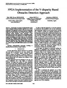
fingerprint, face recognition, facial expressions, voice, iris,… etc. as shown in Fig. 2.1. For this purpose, These methods based on physical or behavioral characteristics are of interest because people cannot forget or lose their physical characteristics [39].
Fig. 2.1: Examples of biometric characteristics: (a) DNA, (b) ear, (c) face, (d) facial thermogram, (e) hand thermogram, (f) hand vein, (g) fingerprint, (h) gait, (i) hand geometry, (j) iris, (k) palmprint, (l) retina, (m) signature, and (n) voice [34].
- 14 -
Chapter 2
Biometric Security Systems
2.3 Biometric History The science of using humans for the purpose of identification dates back to the 1870s and the measurement system of Alphonse Bertillon. Bertillon’s system of body measurements, including skull diameter and arm and foot length, was used in the USA to identify prisoners until the 1920s [40]. Before that, Henry Faulds, William Herschel and Sir Francis Galton proposed quantitative identification through fingerprint and facial measurements in the 1880s. The development of digital signal processing techniques in the 1960s led immediately to work in automating human identification. Speaker [41] and fingerprint [42] recognition systems were among the first to be applied. The potential for application of this technology to high-security access control, personal locks and financial transactions was recognized in the early 1960s. The 1970s saw development and deployment of hand geometry systems [43], the start of large-scale testing and increasing interest in government use of these “automated personal identification” technologies. Then, Retinal [44] and signature verification [45] systems came in the 1980s, followed by face systems [46]. Lastly, Iris recognition [21] systems were developed in the 1990s [33].
2.4 Biometric Characteristic Requirements It is important to distinguish between the human measures as physiological and behavioral characteristics. A physiological characteristic is a relatively stable human physical characteristic, such as a fingerprint, hand geometry, iris pattern, or voiceprint. This type of measurement is unchanging and unalterable without significant duress [31].
Human physiological and/or behavioral characteristic cannot be used as a biometric characteristic unless it satisfies the following requirements [32, 39]: - 15 -
Chapter 2
Biometric Security Systems
(i) Universality (availability), each person should have the characteristic. Which mean that the entire population should ideally have this measure in multiples. (ii) Distinctiveness, means any two persons should be sufficiently different in terms of the characteristic. (iii) Permanence (robustness), the characteristic should be sufficiently invariant (with respect to the matching criterion) over a period of time which means the stability over age. (iv)
Collectability
(accessible),
the
characteristic
can
be
measured
quantitatively. And easy to image using electronic sensors. However, in a practical biometric system (i.e., a system that employs biometrics for personal recognition), there are a number of other issues that should be considered, including [47]: (i) performance, which refers to the achievable recognition accuracy and speed, the resources required and the operational and environmental factors that affect the accuracy and speed; (ii) Acceptability, which indicates the extent to which people are willing to accept the use of a particular biometric identifier (characteristic) in their daily lives (people do not object to having this measurement taken from them); (iii) Circumvention, which reflects how easily the system can be fooled using fraudulent methods. A biometric system to be practical and reliable, should meet the specified recognition accuracy, speed, and resource requirements. Also not be harm to the users, be accepted by the intended population, and be sufficiently robust to various fraudulent methods and attacks to the system.
Robustness is measured by the False Non-Match Rate (FNMR) -also known as “Type I error”- the probability that a submitted sample will not match the enrollment image [48]. Distinctiveness is measured by the False Match Rate - 16 -
Chapter 2
Biometric Security Systems
(FMR) - also known as “Type II error”– the probability that a submitted sample will match the enrollment image of another user [49]. Availability is measured by the “failure to enroll” rate, the probability that a user will not be able to supply a readable measure to the system upon enrollment. Accessibility can be quantified by the “throughput rate” of the system, the number of individuals that can be processed in a unit time, such as a minute or an hour. Acceptability is measured by polling the device users [33, 50].
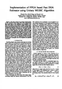
2.5 Biometric Systems As shown in Fig. 2.2, a biometric system consists of several (four basic) components [51]: (i) Sensor module, which acquires the biometric data. An example is a fingerprint sensor. Followed by, (ii) Feature extraction module, where the acquired data is processed to extract feature vectors. For example, the position and orientation of minutiae points (local ridge and valley singularities) in a fingerprint image are extracted. Then, (iii) Matching module, where feature vectors are compared against those in the template. For example, in the matching module of a fingerprint-based biometric system, the number of matching minutiae between the input and the template fingerprint images is determined and a matching score is reported. Finally, (iv) Decision-making module, in which the user's identity is established or a claimed identity is accepted or rejected.
2.5.1 Modes of Operation Depending on the application context, a biometric system may operate in two modes: verification mode or identification mode. In the verification mode, the system verifies the identity by comparing the presented biometric trait by a stored biometric template in the system (one-to-one). If the similarity - 17 -
Chapter 2
Biometric Security Systems
is sufficient according to some similarity measure, the user is accepted by the system. In such a system, an individual who desires to be recognized claims an identity, usually via a Personal Identification Number (PIN), a user name, or a smart card, and the system conducts a one-to-one comparison to determine whether the claim is true or not (e.g., “Does this biometric data belong to this person (x)?”). Identity verification is typically used for positive recognition, where the aim is to prevent multiple people from using the same identity [30, 32]. In the identification mode, database search is crucial and needed. A user presents a not necessarily known sample of his/her biometrics to the system. This sample is then compared with existing samples in a – central - database (one-to-many) [48]. Identification is a critical component in negative recognition applications, where the system establishes whether the person is who he/she (implicitly or explicitly) denies to be. The purpose of negative recognition is to prevent a single person from using multiple identities. Identification may also be used in positive recognition for convenience (the user is not required to claim an identity). While traditional methods of personal recognition such as passwords, PINs, keys, and tokens may work for positive recognition, negative recognition can only be established through biometrics [39].
Fig.2.2: A components of biometric system [51].
- 18 -
Chapter 2
Biometric Security Systems
2.6 A Brief Overview of Commonly Used Biometrics A number of biometric characteristics exist and in use (some commercial, some "not yet"), each biometric has its strengths and weaknesses, and the choice depends on the application. In other words, no biometric is “optimal”; a brief introduction to the commonly used biometrics is given below.
2.6.1 Physiological Characteristic Biometrics (i) Facial, hand, and hand vein infrared thermogram, A pattern of radiated heat from human body considers a characteristic of an individual. These samples of patterns can be captured by an infrared camera in an unobtrusive manner like a regular (visible spectrum) photograph. The technology could be used for covert recognition. A thermogram-based system is noninvasive as it does not require contact, a problem facing image acquisition is challenging in uncontrolled environments, where heat emanating surfaces (e.g., room heaters and vehicle exhaust pipes) are present in the vicinity of the body. A related technology using near infrared imaging is used to scan the back of a clenched fist to determine hand vein structure. Also, Infrared sensors are prohibitively expensive which is a factor make wide spread use of the thermograms less [39]. (ii) Odor, for each individual (organism), an odor as a result of its chemical composition spreads around. Acts as it is characteristic and could be used for distinguishing various objects. Acquisition would be done with an array of chemical sensors, each sensitive to a certain group of compounds. Deodorants and parfumes could lower the distinctiveness leading to bad capturing or enrollment [32].
- 19 -
Chapter 2
Biometric Security Systems
(iii) Ear, many researchers suggested that the shape of the ear to be a characteristic. Studying the structure of the approaches is based on matching the distance of salient points on the pinna from a landmark location on the ear. The features of an ear are not expected to be very distinctive in establishing the identity of an individual [39]. No commercial applications based on ear done until now. (iv) Hand and finger geometry, One of the earliest automated biometric systems was installed during late 1960s and it used hand geometry and stayed in production for almost 20 years. Most measurements declare hand geometry is the dimensions of fingers and the location of joints, shape and size of palm. The technique is very simple, relatively easy to use and inexpensive. Hand geometry operates in verification mode well; it cannot be used for identification of an individual from a large population, because hand geometry is not very distinctive. Dry weather or individual anomalies such as dry skin do not appear to have any negative effects on the verification accuracy. This method can find its commercial use in laptops rather easy, but using it in multimodal gives better performance. There are even verification systems available that are based on measurements of only a few fingers instead of the entire hand. These devices are smaller than those used for hand geometry [32, 39]. Further, hand geometry information may not be invariant during the growth period of children. Limitations in dexterity (arthritis) or even jewelry may influence extracting the correct hand geometry information. (v) Fingerprint, A fingerprint is the pattern of ridges and valleys on the surface of a fingertip, the formation of which is determined during the first seven months of fetal creation. Fingerprints of identical twins are different and so are the prints on each finger of the same person. Humans have used fingerprints for personal identification for many centuries and the matching accuracy using fingerprints has been shown to be very high [52]. Nowadays, a fingerprint scanner costs less, when ordered in large quantities and the marginal cost of - 20 -
Chapter 2
Biometric Security Systems
embedding a fingerprint-based biometric in a system (e.g., laptop computer) has become affordable in a large number of applications. The accuracy of the currently available fingerprint recognition systems is adequate for verification systems and small- to medium-scale identification systems involving a few hundred users. Multiple fingerprints of a person provide additional information to allow for large-scale recognition involving millions of identities. Fingerprints of a small fraction of the population may be unsuitable for automatic identification because of genetic factors, aging, environmental, or occupational reasons (e.g., manual workers may have a large number of cuts and bruises on their fingerprints that keep changing) [32]. Also, (especially when operating in the identification mode) there is a problem with the current fingerprint recognition systems is that they require a large amount of computational resources [39]. (vi) Face, Facial images are probably the most common biometric characteristic used by humans to make a personal recognition; It is a nonintrusive method, The most popular approaches to face recognition are based on either: (i) the location and shape of facial attributes such as the eyes, eyebrows, nose, lips and chin, and their spatial relationships, or (ii) the overall (global) analysis of the face image that represents a face as a weighted combination of a number of canonical faces [32]. While the verification performance of the face recognition systems that are commercially available is reasonable, they impose a number of restrictions on how the facial images are obtained, sometimes requiring a fixed and simple background or special illumination. These systems also have difficulty in recognizing a face from images captured from two drastically different views and under different illumination conditions. It is questionable whether the face itself, without any contextual information, is a sufficient basis for recognizing a person from a large number of identities with an extremely high level of confidence. In order for a facial recognition system to work well in practice, it should automatically[53]: (i) detect whether a face is present in the acquired image; - 21 -
Chapter 2
Biometric Security Systems
(ii) locate the face if there is one; and (iii) recognize the face from a general viewpoint (i.e., from any pose) [39]. The applications of facial recognition range from a static, controlled verification to a dynamic, uncontrolled face identification in a cluttered background (e.g., airport) [54]. (vii) Retina, Since the retina is protected in an eye itself, and since it is not easy to change or replicate the retinal vasculature; this is one of the most secure biometric. Retinal recognition creates an eye signature from the vascular configuration of the retina, which is supposed to be a characteristic of each individual and each eye, respectively. Image acquisition requires a person to look through a lens at an alignment target; therefore, it implies cooperation of the subject. Also some medical conditions make retinal scan can reveal as such hinders public acceptance [39]. (viii) Iris, it is the thin circular region of the eye bounded by the pupil and the sclera on either side. The visual texture of the iris is formed during fetal development and stabilizes during the first two years of life. The complex iris texture carries very distinctive information useful for personal recognition. Each iris is distinctive and, like fingerprints, even the irises of identical twins are different [30]. It is extremely difficult to surgically tamper the texture of the iris. Further, it is rather easy to detect artificial irises (e.g., designer contact lenses). The accuracy and speed of currently deployed iris-based recognition systems is promising and point to the feasibility of large-scale identification systems based on iris information [32]. Although, the early iris-based recognition systems required considerable user participation and were expensive, the newer systems have become more user-friendly and cost effective [39]. A commercial iris recognition system is now available. (ix) Palmprint, palms of the human hands contain unique pattern of ridges and valleys as the same as fingerprints. Since palm is larger then a finger, palmprint is expected to be even more reliable than fingerprint. Palmprint scanners need - 22 -
Chapter 2
Biometric Security Systems
to capture larger area with similar quality as fingerprint scanners, so they are more expensive [55]. A highly accurate biometric system could be combined by using a high-resolution palm print scanner that would collect all the features of the palm such as hand geometry, ridge and valley features, principal lines, and wrinkles [32]. Typical feature as fingerprints have. (x) Voice, The features of an individual’s voice are based on the shape and size of the appendages (e.g., vocal tracts, mouth, nasal cavities, and lips) that are used in the synthesis of the sound. These physiological characteristics of human speech are invariant for an individual, but the behavioral part of the speech of a person changes over time due to age, medical conditions (such as a common cold), and emotional state, etc. Accordingly, Voice is a combination of physiological and behavioral biometrics. Voice is also not very distinctive and may not be appropriate for large-scale identification [31]. Two types of voice systems produced. A text-dependent voice recognition system is based on the utterance of a fixed predetermined phrase. A text-independent voice recognition system recognizes the speaker independent of what he speaks. A text-independent system is more difficult to design than a text-dependent system but offers more protection against fraud. Speaker recognition is most appropriate in phone-based applications but the voice signal over phone is typically degraded in quality by the microphone and the communication channel [32]. A disadvantage of voice-based recognition is that speech features are sensitive to a number of factors such as background noise. (xi) DNA, except for the fact that identical twins have identical DNA patterns [32], deoxyribonucleic acid (DNA) is the unique code for one’s individuality. It is one-dimensional (1–D) ultimate code. However, currently used mostly in the context of forensic applications for person recognition. Three issues limit the utility of this biometrics for other applications [39]: 1. Contamination and sensitivity: it is easy to steal a piece of DNA from an unsuspecting subject that can be subsequently abused for an ulterior purpose; - 23 -
Chapter 2
Biometric Security Systems
2. Automatic real-time recognition issues: the present technology for DNA matching requires cumbersome chemical methods (wet processes) involving an expert’s skills and is not geared for on-line noninvasive recognition; and 3. Privacy issues: information about susceptibilities of a person to certain diseases could be gained from the DNA pattern and there is a concern that the unintended abuse of genetic code information may result in discrimination, e.g., in hiring practices.
2.6.2 Behavioral Characteristic Biometrics (i) Gait, Basically, gait is the peculiar way one walks and it is a complex spatio-temporal biometrics. This is one of the newer technologies and is yet to be researched in more detail. Gait is a behavioral biometric and may not remain the same over a long period of time, due to change in body weight or serious brain damage. Acquisition of gait is similar to acquiring a facial picture and may be an acceptable biometric. Since video sequence is used to measure several different movements this method is computationally expensive [32]. It is not supposed to be very distinctive but can be used in some low-security applications. (ii) Keystroke, It is noticed that each person types on a keyboard in a characteristic way. Keystroke dynamics is a behavioral biometric; for some individuals, one may expect to observe large variations in typical typing patterns. This behavioral biometric is not expected to be unique to each individual but it offers sufficient discriminatory information to permit identity verification [32, 39]. Further, the keystrokes of a person using a system could be monitored unobtrusively as that person is keying in information. (iii) Signature, The way a person signs his / her name is known to be characteristic of that individual. Signature is a simple, concrete expression of the unique variations in human hand geometry. Collecting samples for this - 24 -
Chapter 2
Biometric Security Systems
biometric includes subject cooperation and requires the writing instrument. Signatures are a behavioral biometric that change over a period of time and are influenced by physical and emotional conditions of a subject. In addition to the general shape of the signed name, a signature recognition system can also measure pressure and velocity of the point of the stylus across the sensor pad [39]. Table 2.1 provides a brief comparison of the above biometric techniques based on seven factors.
Biometric Characteristic
Universality
Distinctiveness
Permanence
Collectability
Performance
Acceptability
Circumvention
Table 2.1: Comparison of various biometric technologies. [32, 39]
Facial thermogram
H
H
L
H
M
H
L
Hand vein
M
M
M
M
M
M
L
Gait
M
L
L
H
L
H
M
Keystroke
L
L
L
M
L
M
M
Odor
H
H
H
L
L
M
L
Ear
M
M
H
M
M
H
M
Hand geometry
M
M
M
H
M
M
M
Fingerprint
M
H
H
M
H
M
M
Face
H
L
M
H
L
H
H
Retina
H
H
M
L
H
L
L
Iris
H
H
H
M
H
L
L
Palm print
M
H
H
M
H
M
M
Voice
M
L
L
M
L
H
H
Signature
L
L
L
H
L
H
H
DNA
H
H
H
L
H
L
L
* (H: High, M: Medium, L: Low) - 25 -
Chapter 2
Biometric Security Systems
Based on above discussion and comparison for building accurate, speed, and robust biometric system; these are several important reasons which have motivated the current research using iris as a biometric technology. Additionally, iris has features that make this modality appropriate for recognition purposes: (i) Straightforward iris image capture. (ii) Its universality, most users have one or two irises. (iii) The acceptance by users of all ethnics and different cultures. (iv) The reliability of this modality for large scale identification. (v) This modality has shown in tests the robustness of the algorithms for recognition. And therefore, do not require high performance devices.
2.7 Performance of Biometric Systems. Two samples of the same biometric characteristic from the same person (e.g., two impressions of a user’s right index finger) are not exactly the same due to some reasons like [33,39]: (i) Acquiring sensor (e.g. finger placement). (ii) Imperfect imaging conditions (e.g. sensor noise and dry fingers). (iii) Environmental changes (e.g. temperature and humidity). (iv) Changes in the user’s physiological or behavioral characteristics (e.g. cuts and bruises on the finger). (v) Noise and bad user's interaction with the sensor (e.g. finger placement). It is impossible that two samples of the same biometric characteristic, acquired in different sessions, exactly coincide [56]. For the reason a biometric matching systems' response is typically a matching score (s) (normally a single number) that quantifies the similarity between the input and the database template representations.
- 26 -
Chapter 2
Biometric Security Systems
The higher the score, the more certain is the system that the two biometric measurements come from the same person. The threshold (t) regulates the system decision. The distribution of scores generated from pairs of samples from different persons is called an impostor distribution, and the score distribution generated from pairs of samples of the same person is called a genuine distribution [32]. Fig.2.3 illustrates that fact. A biometric verification system makes two types of errors [39]: (i) Mistaking biometric measurements from two different persons to be from the same person called false match (FMR). (ii) Mistaking two biometric measurements from the same person to be from two different persons called false non-match (FNMR). These two types of errors are often termed as false accept and false reject, respectively. There is a tradeoff between false match rate (FMR) and false non-match rate (FNMR) in every biometric system. In fact, both FMR and FNMR are functions of the system threshold (t); if is decreased to make the system more tolerant to input variations and noise, then FMR increases. On the other hand, if is raised to make the system more secure, then FNMR increases accordingly [57]. The system performance at all the operating points (thresholds) can be depicted in the form of a Receiver Operating Characteristic (ROC) curve. ROC curve is a plot of FMR against (1-FNMR) or FNMR for various threshold values. Fig. 2.4 shows the ROC trade off between security and tolerant (reliability). There are two other recognition error rates that can be also used and they are: Failure to Capture (FTC) and Failure to Enroll (FTE). FTC denotes the percentage of times the biometric device fails to automatically capture a sample when presented with a biometric characteristic. This usually happens when system deals with a signal of insufficient quality. The FTE rate denotes the percentage of times users cannot enroll in the recognition system [32, 51].
- 27 -
Chapter 2
Biometric Security Systems
Fig.2.3: Biometric system error rates. (a) FMR and FNMR for a given threshold t are displayed over the genuine and impostor score distributions; FMR is the percentage of non mate pairs whose matching scores are greater than or equal to t, and FNMR is the percentage of mate pairs whose matching scores are less than t.[32].
Fig. 2.4: Receiver operating characteristic (ROC) [34].
The equal error rate measure, or ERR, is another performance measure that is defined at the point where False Reject Rate (FRR) and False Accept Rate (FAR) are equal [30, 32, 39, 56].
- 28 -
Chapter 3
Human Vision System
Chapter 3
Human Vision System The chapter introduces the human vision system, the iris recognition system phases, and the effect of medical conditions upon the iris capturing. The system challenges, advantages, and disadvantages of the iris recognition system will be under observation to present the importance difficulties of iris recognition system.
3.1 Eye Anatomy It is useful to consider briefly the eye anatomy, which is clearly shown in Fig. 3.1 that states the most important parts of the human eye [58].
Fig. 3.1: Anatomy of the human eye [58].
We will move quickly over only some of the well-known parts of the human eye. The cornea is a clear, transparent portion of the outer coat of the eyeball through which light passes to the lens. The lens helps to focus light on the retina, which is the innermost coat of the back of the eye, formed of light sensitive nerve endings that carry the visual impulse to the optic nerve. The retina [59] acts as a film of a camera in its operation and tasks. - 29 -
Chapter 3
Human Vision System
The iris is a thin circular ring lies between cornea and the lens of the human eye. A front-on view of the iris is shown in Fig. 3.2; in which iris encircles the pupil; the dark centered portion of the eye. The function of iris is to control the amount of light entering through the pupil, this done by the sphincter and dilators muscles, which adjust the size of the pupil [60].
Fig. 3.2: The human iris front-on view [30].
The sphincter muscle lies around the very edge of the pupil. In bright light, the sphincter contracts, causing the pupil to constrict. The dilator muscle runs radially through the iris, like spokes on a wheel. This muscle dilates the eye in dim lighting [30]. The sclera, a white region of connective tissue and blood vessels, surrounds the iris. The externally visible surface of the multi-layered iris contains two zones, which often differ in color [30, 60]. An outer ciliary zone and an inner pupillary zone, and these two zones are divided by the collarette, which appears as a zigzag pattern.
- 30 -
Chapter 3
Human Vision System
The human iris begins to form in the 3rd month of gestation and the structures creating the pattern are complete by the 8th month; the color and pigmentation continue to build through the first year of birth [61]. This pattern contains many distinctive features such as arching ligaments, furrows, ridges, crypts, rings, corona, freckles, and zigzag collarette [62]. As shown in Fig. 3.3. The color of the iris can change as the amount of pigment in the iris increases during childhood. Nevertheless, for most of a human’s lifespan, the appearance of the iris is relatively constant. Therefore, this pattern remains stable through a person's life.
Fig. 3.3: Anatomy of the iris visible in an optical image [33].
The iris is composed of several layers; the visual appearance of the iris is a direct result of its multilayered structure [33]. Iris color results from the differential absorption of light impinging on the pigmented cells in the anterior border layer, posterior epithelium and is scattered as it passes through the stroma to yield a blue appearance. Progressive levels of anterior pigmentation lead to darker colored irises [62]. The average diameter of the iris is nearly 11 mm and the pupil radius can range from 0.1 to 0.8 of the iris radius [62]. It shares high-contrast boundaries with the pupil but less-contrast boundaries with the sclera [61]. - 31 -
Chapter 3
Human Vision System
Formation of the unique patterns of the iris is random and not related to any genetic factors [21]. The only characteristic that is dependent on genetics is the pigmentation of the iris, which determines its color. Due to that the two eyes of an individual contain completely independent iris patterns (left eye is not the same as right one), and it should not verified by an example [63] even they were twins. The false accept probability can be estimated at one in 1031 [62].
3.2 Iris Recognition Systems The idea of using the iris as a biometric is over 100 years old. However, the idea of automating iris recognition is more recent. In 1987, Flom and Safir [64] obtained a patent for an unimplemented conceptual design of an automated iris biometrics system [30]. Image processing techniques can be used to extract the unique iris pattern from a digitized image of the eye, and encode it into a biometric template, which can be stored in a database later. This biometric template contains an objective mathematical representation of the unique information stored in the iris, and allows comparisons to be made between templates. When a subject wishes to be identified by an iris recognition system, their eye is first photographed (captured by camera, this step called acquisition stage), and then a template created for their iris region (these stages will be explained later). This template is then compared with the other templates stored in a database until either a matching template is found and the subject is identified, or no match is found and the subject remains unidentified. In addition, iris recognition system works in the two modes: verification and identification, which had been illustrated in chapter 2.
- 32 -
Chapter 3
Human Vision System
3.3 Medical Conditions Affecting Iris Pattern. Various medical conditions may result in such problems: A cataract is a clouding of the lens, the part of the eye responsible for focusing light and producing clear, sharp images. Cataracts are a natural result of aging: ‘‘about 50% of people aged 65–74 and about 70% of those 75 and older have visually significant cataracts’’ [65]. Eye injuries, certain medications, and diseases such as diabetes and alcoholism have also been known to cause cataracts. Cataracts can be removed through surgery. Patients who have cataract surgery may be advised to re-enroll in iris biometric systems. Glaucoma refers to a group of diseases that reduce vision. The main types of glaucoma are marked by an increase of pressure inside the eye. Pressure in the eye can cause optic nerve damage and vision loss. Glaucoma generally occurs with increased incidence as people age [65] as same as cataract be. Two conditions that relate to eye movement are nystagmus and strabismus. ‘‘Strabismus, more commonly known as cross-eyed or wall-eyed, is a vision condition in which a person cannot align both eyes simultaneously under normal conditions’’ [66]. Nystagmus involves an involuntary rhythmic oscillation of one or both eyes, which may be accompanied by tilting of the head. Albinism is a genetic condition that results in the partial or full absence of pigment (color) from the skin, hair, and eyes [33]. The conditions of nystagmus and strabismus are associated with albinism. Approximately 1 in 17,000 people are affected by albinism [67].
- 33 -
Chapter 3
Human Vision System
Another relevant medical condition is aniridia, which is caused by a deletion on chromosome (no. 11) [68]. In this condition, the person is electively born without an iris, or with a partial iris. The pupil and the sclera are present and visible, but there is no substantial iris region. Aniridia is estimated to have an incidence of between 1 and 50,000 and 1 and 100,000. This may seem rare especially in our country (Egypt). As the examples of these diseases illustrated, it is disadvantages in the deployment of iris biometrics on a national scale. This is a problem that has to date received little attention in the biometrics research community. This problem could partially be addressed by using multiple biometric modes [69].
3.4 Iris System Challenges One of the major challenges of automated iris recognition systems is to capture a high quality image of iris while remaining noninvasive to the human operator. Moreover, capturing the rich details of iris patterns, an imaging system should resolve a minimum of 70 pixels in iris radius. In the field trials to date, a resolved iris radius of 80–130 pixels has been more typical. Monochrome CCD cameras (480×640) have been widely used because Near Infrared (NIR) illumination in the 700–900-nm band was required for imaging to be non-intrusive to humans. Some imaging platforms deployed a wide-angle camera for coarse localization of eyes in faces; to steer the optics of a narrowangle pan/tilt camera that acquired higher resolution images of eyes [62]. Given that iris is a relatively small (nearly 1 cm in diameter), dark object and that human operators are very sensitive about their eyes; this matter required careful engineering. Some points should be taken into account: (i) Acquiring images of sufficient resolution and sharpness; (ii) Good contrast in the interior iris pattern without resorting to a level of illumination that annoys - 34 -
Chapter 3
Human Vision System
the operator; (iii) The images should be well framed (i.e. centered), and (iv) Noises in the acquired images should be eliminated as much as possible.
3.5 Advantages of Iris Systems Iris recognition is especially attractive due to high degree of entropy per unit area of iris; as well as, the stability of iris texture patterns with age and health conditions. Moreover, there are several advantages of iris [70]: (i) an internal organ, it is visible thanks to the transparent lens which covers it; (ii) mostly flat with muscles; which control the diameter of the pupil; (iii) no need for a person to be identified to touch any equipment that has recently been touched by strangers; (iv) Surgical procedures do not change the texture of the iris; (v) immensely reliable, and (vi) It has responsive nature. For such reasons beside the briefly ones discussed in chapter two; the iris chosen as our biometric technology for recognition system; as it is the most accurate and reliable as recent researches demonstrate.
3.6 Disadvantages of Iris Systems However, there are some disadvantages of using iris as a biometric measurement are [71]: (i) Small target (1-cm) to acquire from a distance (about 1-m) therefore it is hard to detect from a distance; (ii) Illumination should not be visible or bright; (iii) The detection of iris is difficult when the target is moving; (iv) The cornea layer is curved; (v) Eyelashes, corrective lens and reflections may blur iris pattern, it also Partially occluded by eyelids, often drooping; (vi) Iris will deform non-elastically when the pupil changes its size, and (vii) Iris scanning devices are very expensive.
- 35 -
Chapter 4
Iris Database and Dataset
Chapter 4
Iris Database and Dataset This chapter describes briefly the common datasets used, concentrating on Chinese Academy of Sciences Institute of Automation (CASIA 1) that is used in current research. These database characteristics will be illustrated through the literature.
4.1 Iris Image Acquisitions All current commercial iris biometrics systems still have constrained image acquisition conditions. Near infrared illumination, in the 700–900 nm range, is used to light the face, and the user is prompted with visual and/or auditory feedback to position the eye so that it can be in focus and of sufficient size in the image [30]. In 2004, Daugman suggested that the iris should have a diameter of at least 140 pixels [62]. The International Standards Organization (ISO) Iris Image Standard released in 2005 is more demanding, specifying a diameter of 200 pixels [72]. Experimental research on iris recognition system requires an iris image dataset. Several datasets are discussed briefly in this chapter.
4.2 Brief Descriptions of Some Datasets There is not any public iris database. Lacking of iris data may be a block to the research of iris recognition. To promote the research, National Laboratory of Pattern Recognition (NLPR), Institute of Automation (IA), Chinese Academy of Sciences (CAS) provide iris database freely for iris recognition researchers. Table 4.1 summarizes information on a number of famous iris datasets. - 36 -
Chapter 4
Iris Database and Dataset
Table 4.1: Mostly used iris databases
No. of
No. of
irises
images
CASIA 1
108
756
CASIA camera
CASIA 3
1500
22051
CASIA camera and OKI irispass-h
ICE 2005
244
2953
LG2200
ICE 2006
480
60000
LG2200
MMU 1
90
450
LG IrisAccess
MMU 2
199
995
Panasonic BM-ET100US Authenticam
UBIRIS
241
1877
Nikon E5700
UPOL
128
384
SONY DXC-950P 3CCD
Database
Camera used
4.2.1 Chinese Academy of Sciences - Institute of Automation (CASIA version 1) All images tested are taken from the Chinese Academy of Sciences Institute of Automation (CASIA) iris database, apart from being the oldest [73]; this database is clearly the most known and widely used by the majority of researchers. Beginning with a 320×280 pixel photograph of the eye took from 4 cm away using a near infrared camera. The NIR spectrum (850 nm) emphasizes the texture patterns of iris making the measurements taken during iris recognition more precise. CASIA database (version.1) includes 756 iris images from 108 eyes, hence 108 classes. For each eye, 7 images were captured; in two sessions, where 3 samples are collected in the first and 4 samples in the second session [74]. Images have been captured under highly constrained environment. They present very close and homogeneous characteristics and their noise factors are exclusively related with iris obstructions by eyelids and eyelashes; as shown in - 37 -
Chapter 4
Iris Database and Dataset
Fig. 4.1 the pupil regions of all iris images were automatically detected and replaced with a circular region of constant intensity to mask out the specular reflections from the NIR illuminators (8 illuminators) before public release.
Fig. 4.1: Example iris images in CASIA-IrisV1: from two different sessions [74].
4.2.2 Iris Challenge Evaluation (ICE) The iris image datasets used in the Iris Challenge Evaluations (ICE) in 2005 and 2006 [75] were acquired at the University of Notre Dame, and contain iris images of a wide range of quality, including some off-axis images. The ICE 2005 database is currently available, and the larger ICE 2006 database also released. One unusual aspect of these images is that the intensity values are automatically contrast-stretched by the LG 2200 to use 171 gray levels between 0 and 255. Samples are shown in Fig. 4.2.
Fig. 4.2: Example iris images in ICE-2006 [75].
- 38 -
Chapter 4
Iris Database and Dataset
4.2.3 Lions Eye Institute The Lions Eye Institute (LEI) database [76] consists of 120 greyscale eye images taken using a slit lamp camera. Since the images were captured, using natural light, specular reflections are present on the iris, pupil, and cornea regions. Unlike the CASIA database, the LEI database was not captured specifically for iris recognition.
4.2.4 Multimedia University (MMU 1 and MMU 2) MMU1 iris database contributes a total number of 450 iris images, which were taken using LG IrisAccess®2200. This camera is semi-automated and it operates at the range of 7-25 cm. On the other hand, MMU2 iris database consists of 995 iris images. The iris images are collected using Panasonic BMET100US Authenticam and its operating range is even farther with a distance of 47-53 cm away from the user. These iris images are contributed by 100 volunteers with different age and nationality. They come from Asia, Middle East, Africa and Europe. Each of them contributes 5 iris images for each eye. There are 5 left eye iris images, which are excluded from the database due to cataract disease [77]. Fig. 4.3 shows some samples of these iris images.
Fig. 4.3: Example iris images in MMU 1 [77].
- 39 -
Chapter 4
Iris Database and Dataset
4.2.5 University of Bath Iris Image Database (UBIRIS) UBIRIS version 1 is a version of the database is collected from 241 persons during September 2004 in two distinct sessions. Its most relevant characteristic is to incorporate images with several noise factors, simulating less constrained image acquisition environments. This enables the evaluation of the robustness of iris recognition methods. For the first image capture session, the enrollment one, noise factors minimized, especially those relative to reflections, luminosity and contrast, having installed image capture framework inside a dark room. In the second session, the capture place changed in order to introduce natural luminosity factor. This propitiates the appearance of heterogeneous images with respect to reflections, contrast, luminosity and focus problems. Images collected at this stage simulate the ones captured by a vision system without or with minimal active participation from the subjects, adding several noise problems. These images will be on the recognition stage compared to the ones collected during first session [78]. However, the second version of the UBIRIS database has over 11000 images (and continuously growing) and more realistic noise factors. Images were actually captured at-a-distance and on-the-move and on the visible wavelength), with corresponding more realistic noise factors. See fig. 4.4, some random samples are in present.
Fig. 4.4: Example iris images in UPIRIS [78]
- 40 -
Chapter 4
Iris Database and Dataset
4.3 Dataset Used In this thesis, the CASIA (version 1) iris image database is used for the testing and experimentation. Such the images, taken in almost perfect imaging conditions, are noise-free (photon noise, sensors noise & electrons, reflections, focus, compression, contrast levels, and light levels).
In addition, using NIR illumination helps in illumination to be controlled and unintrusive to humans, and helps reveal the detailed structure of heavily pigmented (dark) irises too. A random subset database of different person's eyes is selected for test, under unbiased conditions. This will be discussed later in chapter six.
- 41 -
Chapter 5
Image Processing Algorithm
Chapter 5
Image Preprocessing Algorithm This
chapter
includes
our
proposed
system
and
software
implementation. It will discuss the image pre-processing methods. It browses the image processing steps. In addition, the segmentation processes based on the modifications of Wildes and daugman approaches. Iris normalization and unwrapping method this images results review. The results of each step will be drawn in the end of its section.
5.1 Proposed Iris Recognition System A general iris recognition system is composed of four steps shown in Fig. 5.1. Firstly, image acquisition as the user's eye is captured by the system. Using CCD cameras (480×640) by near infrared (NIR) illumination in (700-900 nm) or by standard cameras (i.e. Panasonic BMET 100). Then the image is preprocessed to normalize the scale and illumination of the iris localizing the iris. Thirdly, features representing the iris patterns are extracted and quantized. Finally, decision is made by using template-matching techniques for iris code generation [79].
Fig. 5.1: Stages of iris recognition algorithm.
- 42 -
Chapter 5
Image Processing Algorithm
During this work, all advantages of current iris processing algorithms gained and combined as well as new trends in image processing algorithms in order to get a system that satisfies: (i) More accurate iris code generation; (ii) Simple iris normalization; (iii) Accurate iris and pupil detection; (iv) Simple quantization process, as well as, and (v) Fast iris processing system; which will enable us to build a real time iris recognition system. The phases of software system is shown in Fig. 5.2; the original eye image was presampled to (260×320) pixels to crop the unneeded parts of the eye image, as well as to decrease the processing time during the pupil boundary (iris inner boundary) detected [80]. Through feature extraction process, 1D log-Gabor used and so the verification associated results compared by the ones handled by using DCT to achieve the best accurate method.
Iris Image Preprocessing Iris image
Pupillary
Localization
Iris area
Localization
of iris
isolation
Normalization
Normalized Iris Template Matching
Feature Vector
Feature Extraction 1D Log-Gabor
(Hamming Distance)
Enhancement
DCT Fig. 5.2: Block diagram of iris recognition system.
5.2 Iris Localization One of the most important steps in iris recognition systems is iris localization, which aims to detect the exact location and contour of the iris in eye image. The performance of the identification system is closely related to - 43 -
Chapter 5
Image Processing Algorithm
the precision of the iris localization step. Most of previous iris segmentation approaches assume that the boundary of pupil and iris is a circle. So to detect the boundary, the center and radius needed for the pupil circle and for iris circle. However, note that the two centers do not have the same coordinates.
5.2.1
Detecting the Pupil Boundary
Since the pupil generally is the darkest region in the image, this approach applies threshold segmentation method to find the region [79, 81]. Firstly,
standout iris-pupil
by contrasting,
using thresholding linear
transformation. Then filter bright pixels by using threshold brightness (in our implementation is 200). After that, approximate center of pupil using weight centriod of pixels and radius calculated from the maximum circular summation of gradient points into the circle. Steps illustrated in Fig. 5.3 sequentially.
(a)
(b)
(c)
Fig. 5.3: Pupil boundary detection steps: (a) Original eye image (260*320). (b) Pupil after threshold (200). (c) The segmented pupil (centre coordinate (163,135) and radius (36 pixels)).
5.2.2 Detecting the Iris Boundary The pupil center can be used to detect the approximate inner and outer iris boundaries. Wildes [21], Kong and Zhang, and Ma et al. [82] use Hough Transform on the binary edge map to localize iris. Daugman [62] uses an - 44 -
Chapter 5
Image Processing Algorithm
integro-differential operator on the raw image to isolate the iris, also in pupil detection.
5.2.2.1
John Daugman Approach
The method localize iris is based on the integro-differential operator finding the pupillary boundary and the limbus boundary as circles (with three parameters: the radius (r), and the coordinates of the center of the circle (x0 , y0.) Then eyelids boundaries, using the same approach with arcs. His operator is max( r , x 0 , y o ) G (r ) *
r
r , x0 , y0
I ( x, y ) ds 2r
(5.1)
where Gσ (r) is a smoothing function and I(x, y) is the image of the eye. This function finds for an image I(x,y), the maximum of the absolute value of the convolution of a smoothing function Gσ with the partial derivative, with respect to ( r ), of the normalized contour integral of the image along an arc (ds) of a circle. The symbol * denotes convolution and Gσ is a smoothing function such as a Gaussian of scale σ [30, 62]. This operator searches for the circular path where there is maximum change in pixel intensity, by varying the radius r and center x and y position of the circular contour. Then applied iteratively with the amount of smoothing progressively reduced in order to attain precise localization.
The deficiency of this approach, in cases where there is noise in the eye image, such as from reflections, this integro-differential operator fails; this is due to the fact that it works only on a local scale. Another deficiency of this operator is that it is too computationally exhaustive. However, since the integro-differential works with raw derivative information, it does not suffer from the thresholding problems of the Hough transform [30]. - 45 -
Chapter 5
Image Processing Algorithm
5.2.2.2
Richard Wildes Approach
Wildes [21] system performs its iris localization in two steps: STEP-1: Binary edge mapping. An edge detector operator is applied to a gray scale iris image to generate the edge map. The edge map is obtained by calculating the first derivative of intensity values and threshold the results. After that, a Gaussian filter; zero mean and unit variance, is applied to smooth the image to select the proper scale of edge analysis [1]. Once Classical operators work very well on high-contrast images [83], and CASIA (ver.1) images achieve this property; Canny edge detector is used to generate the edge map with parameters (threshold=0.1 and sigma=1) to reduce edge points with from the edge map. The algorithm runs in 5 separate steps [84, 85]: (i) Smoothing, by convoluting it with a Gaussian smoothing filter
Blurring of the image to
remove noise; (ii) Finding gradients, gradient magnitude is computed using two 2x2 convolution masks; (iii) Non-maximum suppression, Only local maxima should be marked as edges. An edge point is a pixel whose strength is locally maximum in the direction of the gradient. The result of this step is data that is almost zero everywhere except at local maxima points; (iv) Double thresholding, incorrect choice of the threshold might easier cause detection of false edges or exclusion of some. To overcome this problem, two threshold values are applied to the data (one is double the other), and (v) Edge tracking by hysteresis, Final edges are determined by suppressing all edges that are not connected to a very certain (strong) edge.
STEP-2: Voting via Circular Hough Transform (CHT). The Hough transform is algorithm can be used to detect and determine the parameters of simple geometric objects (shapes), such as lines, circles, parables, and ellipses or any other arbitrary shape. From the edge map, votes are cast in Hough space for the parameters of circles passing through each edge - 46 -
Chapter 5
Image Processing Algorithm
point, in order to search for the desired contour from the edge map. The Hough transform for a circular boundary and a set of recovered edge point (xj, yj): j=1, 2, … n is defined as [82]: n
H(xc, yc, r) h(xj , yj , xc, yc, r)
(5.2)
j 0
Where
1, h(xj , y j , xc , yc , r) 0,
if g(x j , y j , xc , yc , r) 0 otherwise
And
g(xj , yj , xc, yc, r) (xj xc)2 (yj yc)2 r2 Where (xc, yc) is the center coordinate of the circle with radius r. so, each edge point on the circle casts a vote in Hough space. The center coordinate and radius of the circle with maximum number of votes is defined as the contour of interest [79]. Wildes et al. [86, 87], in performing edge detection, bias the derivatives in the vertical direction for detecting the outer circular boundary of the iris, and in the horizontal direction for detecting the eyelids. For eyelids detection, the contour is defined using parabolic curve parameter instead of the circle parameter. The disadvantage of Hough transform algorithm, firstly it is computationally intensive, leading to low speed efficiency due to its ‘bruteforce’ approach. But, less than integro-differential operator. Secondly, it requires a threshold value to generate the edge map. And this may result in critical edge points being removed, and result in false circle/arc detection [88]. So it fails to detect some circles. However, on other hand, Hough transform is unaffected by noise and provides more accuracy in localization than Daugman's algorithm, it detects the outer iris boundary in a much more efficient method than the integro-differantial equation based techniques.
- 47 -
Chapter 5
Image Processing Algorithm
5.2.2.3
Proposed Algorithm for Iris Segmentation
In order to get over the drawbacks of above approaches, mixed techniques were described to implement an iris segmentation. The segmentation stage is critical to the success of an iris recognition system, and data that is falsely represented as iris pattern data will corrupt the biometric templates generated, resulting in poor recognition rates, Wildes approach chosen to localize the iris, but some modifications occurred. First, we detected the pupil by thresholding techniques after presampling eye image. Then detect the iris boundary using CHT. For the CASIA database, values of the iris radius range from 90 to 150 pixels. Therefore, after canny edge detection, iterations of circles drawing in Hough matrix space in range two values (100-130) occur. In addition, we considered the small area occluded by eyelids and random scattering of eyelashes, which is darker as pupil. It could be considered as a part of iris code and the iris region is small size rich data. That means removing random scattering eyelashes will reduce the iris data signature. After running the segmentation phase, iris isolation done giving pupil circle (center coordinate and radius) and iris circle too. These parameters used in iris normalization and unwrapping next stage. Daugman's rubber sheet model used instead of Wildes normalized spatial correlation for matching using image registration technique [21] based on its simplicity. Result of localization processes is illustrated in Fig. 5.4 and some random samples of iris segmentation test are shown in Fig. 5.5.
- 48 -
Chapter 5
Image Processing Algorithm
(a)
(b)
(c)
(d)
Fig. 5.4: Iris localization steps: (a) edge after canny detector; (b) Hough space of CHT; (c) The segmented iris; (d) Final iris isolated region.
Fig. 5.5: Result of the proposed segmentation algorithm. (The upper images are a pupil and iris detection, and the lower ones represent the final iris localization for each one respectively).
5.3 Iris Normalization and Unwrapping Once the iris region is segmented and isolated, the next stage is to normalize this part to enable the generation of the iris code and their comparisons between different irises. We should transform the extracted iris region so that it has fixed dimensions [62]. In addition, the normalization is useful as that the representation is common to all, with similar dimensions.
- 49 -
Chapter 5
Image Processing Algorithm
The reason lets normalization and unwrapping necessary is sources of inconsistency include: (i) Dimensional inconsistencies due to the stretching of the iris caused by the pupil dilation from varying levels of illumination[89], because Pupil is very sensitive to illumination, so if illumination changes the pupil size of same eye varies; (ii) Varying imaging distance tends to capture the images in different size, that affect in recognition result; (iii) Rotation of the camera; (iv) Head tilt; (v) Rotation of the eye at capturing, and (vi) In addition, the pupil region is not always concentric within the iris region, and is usually slightly nasal.
Upon above, the iris region needs to be normalized to compensate for these all states, which achieve by Daugman's Rubber Sheet Model. The normalization process will produce iris regions, which have the same constant dimensions, so that two images of the same iris under different capture conditions will have characteristic features at the same spatial location. Normalization also reduces the distortion caused by pupil movement. The normalization process involves unwrapping the iris and converting it into its polar equivalent. It is done using Daugman’s rubber sheet model [60]. The center of the pupil is considered as the reference point acts as the center of the swapping ray, and a remapping formula is used to convert the points on the Cartesian scale to the polar scale [90]. Rubber sheet model proposed by Daugman [19, 63] remaps each point within iris region from (x,y) Cartesian coordinates to a pair of normalized non-concentric polar coordinates (r, θ) where r is on the interval [0, 1] and θ is angle [0, 2π] as:
I(x(r,),y(r,))I(r,)
(5.3)
where x(r, θ) and y(r, θ) are defined as linear combinations of both the set of pupillary boundary points (xp(θ),yp(θ)) and limbos boundary points (xi(θ),yi(θ)) where[91]: - 50 -
Chapter 5
Image Processing Algorithm
x(r,) (1r)xp()rxi ()
(5.4)
y(r, ) (1 r) yp () ryi ()
(5.5)
This model defines iris code in two ways of polar coordinates [60, 89, 90], a number of data points are selected along each radial line defined as the radial resolution, and the number of radial lines going around the iris region is defined as the angular resolution. It does not compensate for rotational inconsistencies, so rotation is accounted for during Daugman's matching phase by shifting the iris templates in the θ direction until two iris templates are aligned [19] before Hamming distance applied, to give a decision. Due to the fact that pupil is non-concentric to the iris, so in implementation process, a remapping formula is needed to rescale points depending on the angle around the circle as mentioned in fig. 5.6 This is given by[92]: r ' 2 ri
2
(5.6)
With ox 2 o y 2 o cos arctan y o x
Where ox, oy represent the displacement of the centre of the pupil relative to the centre of the iris, and (r') represents the distance between the edge of the pupil and edge of the iris at an angle θ around the region, and ri is the radius of the iris.
- 51 -
Chapter 5
Image Processing Algorithm
Fig. 5.6: Implementation of unwrapping step.
After unwrapping phase, a 2D array with vertical dimensions of radial resolution (46 pixels) and horizontal dimensions of angular resolution (512 pixels) produced. Fig. 5.7 illustrates Daugman rubber sheet model and our normalization result under angular resolution of 512 and radial resolution of 46. Also, fig. 5.8 declares the iris after unwrapping process generated after segmentation phase. Values at the boundary of the pupil-iris border, and the iris-sclera border are discarded, as these non-iris region data and will introduce noise in iris template.
(a)
(b)
Fig. 5.7: Unwrapping and normalization: (a) Daugman Rubber Sheet model [90] and (b) Unwrapped iris image (angular resolution of 512 and radial resolution of 46).
- 52 -
Chapter 5
Image Processing Algorithm
Fig. 5.8: A sample results of unwrapping and normalization implementation.
- 53 -
Chapter 6
Iris Code Generation and Matching
Chapter 6
Iris Code Generation and Matching The chapter indicates the iris code generation methods. The enhancements of iris image, followed by feature extraction algorithms based on log-Gabor and DCT will be compared. In addition, Hamming Distance operator will be discussed as the iris classifier. Finally, the results of log-Gabor based system performance and DCT-based one obtained more clearly. Results and discussions will be presented in the end of this chapter.
6.1 Iris Image Enhancement The normalized iris image still has low contrast and may have nonuniform illumination caused by the position of light sources [93]; In order to obtain more well distributed texture image we make enhancement. This can be reached by histogram equalization. The histogram of gray scale image consists of the histogram of its grey levels; that is, a graph indicating the number of times each grey level occurs in the image. Histogram equalization is a technique for adjusting image intensities to enhance contrast. Images with such poor intensity distributions can be helped with this technique, which in essence redistributes intensity distributions [79, 94]. Let f be a given image represented as mr × mc matrix of integer pixel intensities ranging from 0 to L-1. L is the number of possible intensity values, often 256 in gray level images. Let p denote the normalized histogram of f with a bin for each possible intensity [4]. So: pn = Number of pixels with intensity n / Total number of pixels For n = 0, 1, …..., L − 1. The histogram equalized image g will be defined by: - 54 -
(6.1)
Chapter 6
Iris Code Generation and Matching fi, j
gi , j floor ( L 1) Pn
(6.2)
n0
Where floor() rounds down to the nearest integer. Enhanced normalized iris templates shown in fig. 6.1, the upper image is the normalized iris and the lower is its histogram.
(a)
(b)
Fig. 6.1: Enhanced normalized iris template with histogram: (a) original template with its histogram, (b) template after histogram equalization applied.
6.2 Iris Feature Extraction One of the most interesting aspects of the world is that it can be considered to be made up of patterns. A pattern is essentially an arrangement. It is characterized by the order of the elements of which it is made, rather than by the intrinsic nature of these elements [95]. After the iris has been localized, and its associated templates have been generated, iris codes must be generated. In the coding process, the biometric information of the iris texture is extracted from the Enhanced normalized iris image and a unique pattern is generated. In this phase, texture analysis methods are used to extract the most discriminating features used to generate the significant iris code [96]. Only the significant - 55 -
Chapter 6
Iris Code Generation and Matching
features of the iris must be encoded; so we can compare the stored features to the any unknown iris features to see if they are the same or not [30]. The iris pattern provides two types of information: The amplitude information and the phase information. Because of amplitude information depends on many extraneous factors such as imaging contrast, illumination and camera gain; only phase information is used to generate the iris code [97].
Some researchers work using something other than a Gabor filter to produce a binary representation similar to Daugman’s iris code. Sun et al. [98], Ma et al. [26], Chenhong and Zhaoyang [99], Chou et al. [100], and Yao et al. [101] are examples of that. Another work looks at using different types of filters to represent the iris texture with a real-valued feature vector like that of Wildes. An early example of this is the work by Boles and Boashash [102], Sanchez-Avila and Sanchez-Reillo [103], Alim and Sharkas [104], and Ma et al. [25]. A smaller body of work [105,106,107,108] looks at combinations of these two general categories of approach. In this thesis, 1D log-Gabor and DCT are typically used for analyzing the human iris patterns and extracting significant features from them.
6.2.1 1D Log-Gabor Wavelet Most of iris coding systems like Daugman's system [19, 62] make use of Gabor filters, which have proved to be very efficient for image texture, and high accuracy in recognition rate. Gabor filter’s impulse response is defined by a harmonic function multiplied by a Gaussian function [79]; It is constructed by modulating a sine/cosine wave with a Gaussian. It provides optimum localization in both spatial and frequency domains. Decomposition of a signal using Gabor filter is accomplished using a quadrature pair of Gabor filters, with a real part(even symmetric component) - 56 -
Chapter 6
Iris Code Generation and Matching
specified by a cosine modulated by a Gaussian, and an imaginary part(odd symmetric component) specified by a sine modulated by a Gaussian [62]. It is noted that phase information, rather than amplitude information provides the most significant information within an image. Taking only the phase will allow encoding of discriminating information in the iris, while discarding redundant information such as illumination represented by the amplitude component [109]. The Gabor filter in any encoding and an even symmetric will have a DC component whenever the bandwidth is larger than one octave [110]. Therefore the Log-Gabor filters have been recently suggested [111, 90] for phase encoding because of presence the zero DC-component caused by background brightness [112]. It can be obtained for any bandwidth by using a Gabor filter, which is Gaussian on a logarithmic scale. This is known as the Log-Gabor filter. The performance from the Log-Gabor filter is the best when followed by the Haar wavelet, discrete cosine transform (DCT), and Fast Fourier Transform (FFT) [110]. The Log-Gabor filters having extended tails at the high frequency end are expected to offer more efficient encoding of natural images.
The Log-Gabor function has singularity in the log function at the origin, therefore the analytic expression for the shape of the Log-Gabor filter cannot be constructed in spatial domain. Therefore, the filter is implemented in frequency domain, with frequency response defined as follows: (log(f / f ))2 0 G( f ) exp 2(log( f / f0 ))2
(6.3)
With f0 is the central frequency and σf is the scaling factor of the radial bandwidth B [113]. The radial bandwidth in octaves is expressed as follows [24]: - 57 -
Chapter 6
Iris Code Generation and Matching
(6.4)
B 2 2 / ln 2 * ln( f / f 0 )
The selected parameters to achieve the best performance were the center wavelength of 18 and ratio σf /f0 of 0.55. This approach compresses the data to obtain significant data [79]; the compressed data can be stored and processed affectivity. The 2D normalized pattern is broken up into a number of 1D signal (one for each row of the image in frequency domain), and then convolved with 1D Log-Gabor wavelets. Angular direction is taken rather than the radial one, which corresponds to columns of the normalized pattern, since maximum independence occurs in the angular direction. The total number of bits in the template will be the angular resolution times the radial resolution, times 2 ( since Log-Gabor filter is applied to generate the code by assigning two bits per pixel to the corresponding phase of the filtered image), times the number of filters used. It is suitable where the relevant texture information has a bandwidth greater than one octave [96] (an optimal Log-Gabor filter with a bandwidth around two octaves has been selected). that they permit a more compact representation of images.
Fig. 6.2 shows the decomposition of the normalized image and the phase coding. Fig. 6.3 shows the real part of the iris code after log-Gabor filter (since modulation of the sine with a Gaussian provides localization in Space, though with loss of localization in frequency). Total number of bits in iris code
generated using 1D Log-Gabor is 512*46*2 bits.
- 58 -
Chapter 6
Iris Code Generation and Matching
Even
Odd
(a)
(b)
(c)
Fig. 6.2: 1D-Log Gabor filter and encoding idea: (a) Decomposition of the normalized image into a set of 1D signals, (b) Phase coding, and (c ) Transfer function.
(a
(b
Fig. 6.3: Iris code generation: (a) Normalized iris and (b) Encoded iris texture after 1D log-Gabor filter
6.2.2 The Discrete Cosine Transform (DCT) A DCT expresses a sequence of finitely data points in terms of a sum of cosine functions oscillating at different frequencies [114]. The two dimensional DCT (DCT-II) is often used in signal and image processing and can be considered as a direct extension of the 1-D case. It can constitute an integral part of successful pattern recognition system [58]. However, the use of cosine rather than sine functions turns out that cosine functions are much more efficient; due to the following important properties: (i) energy compaction; (ii) decorrelation; (iii) separability; (iv) symmetry; and (v) Orthogonality. The DCT of an N*N image f(x, y), is defined by [115]:
- 59 -
Chapter 6
Iris Code Generation and Matching ( N 1) ( N 1)
F (u , v) C (u )C (v) x 0
f ( x, y ) cos
y 0
(2 x 1)u (2 y 1)v cos 2N 2N
(6.5)
The inverse transform is defined by [116]: ( N 1) ( N 1)
f (u , v)
C (u)C (v) F (u, v) cos x 0
y 0
(2 x 1)u (2 y 1)v cos 2N 2N
(6.6)
Where: C (u ) C (v)
1 , foru, v 0 N
And C (u ) C (v )
2 , foru, v 0 N
In addition, of its strong energy compaction property, the feature extraction capabilities of the DCT coupled with well-known fast computation techniques [117]. It compresses all the energy of the image and concentrates it in a few real valued coefficients located in the upper-left corner of the resulting real-valued M*N DCT/frequency matrix. A coefficient’s usefulness is determined by its variance over a set of images as in video’s case. If a coefficient has a lot of variance over a set, then it cannot be removed without affecting the picture quality. Zero or low-level pixel values except at the topleft corner. These low-frequencies, high-intensity coefficients are therefore, the most important coefficients in the frequency matrix and carry most of the information about the original image [58]. Decorrelation is the principle property of image transformation means the removal of redundancy between neighboring pixels. This leads to uncorrelated transform coefficients, which can be encoded independently. From equation 5, C(u, v) can be computed in two steps by successive 1-D operations on rows and columns of an image. This property, known as separability. Also looking at the row and column operations in the previous equation reveals that these operations are functionally identical. Such a - 60 -
Chapter 6
Iris Code Generation and Matching
transformation is called a symmetric transformation [118]. The useful of the two properties lies in that transformation matrix can be pre-computed offline and then applied to the image thereby providing orders of magnitude improvement in computation efficiency [119]. DCT basis functions are orthogonal. Thus, the inverse transformation matrix of A is equal to its transpose i.e. A-1= AT. Therefore, this property renders some reduction in the pre-computation complexity. A binary template is generated from the zero crossings of the differences between DCT coefficients. Based on DCT properties and experiments, this coding method has low complexity and good interclass separation [79]. It is superior to other approaches in terms of both speed and accuracy. Feature extraction for iris code based on DCT achieves less size extracted normalized iris data codes, due to DCT energy compaction characteristic giving such less time real time implementation. Fig. 6.4 shows the encoded iris texture after DCT transform [120].
Fig. 6.4: Encoded iris texture after DCT transforms.
6.3 Template Matching Both real and imaginary parts of the templates generated from the feature extraction stage are each quantized, converting number feature vector to binary code. As Boolean vectors are always easier to compare and to manipulate. Thus, it is easier to find the difference between two binary codes than between - 61 -
Chapter 6
Iris Code Generation and Matching
two number vectors. In addition, it is useful to store a small number of bits for each iris code. In the comparison stage, a dissimilarity measure is computed between two codes to decide whether the two iris images are the same eye or not. A threshold is needed to differentiate between intra-class and inter-class comparisons [90]. Hamming Distance (HD) employed by Daugman was chosen as a metric for recognition. It represents the number of bits that are different in the two patterns [79]. The hamming distance is defined as followed:
HD
1 N X j ( XOR)Yj N j1
(6.7)
Where X and Y are the two-bit patterns; that we compared and N is the total number of bits. The larger the hamming distance (closer to 1), the more the two patterns are different and the closer this distance is to zero; the more probable the two patterns are to be identical [61]. Therefore, a threshold is set to define the imposter. Daugman set this threshold equal 0.32 [62]. The optimum threshold in our system based on 1D Log-Gabor and DCT is 0.45212 and 0.48553 respectively. This technique for matching is fast because the templates vectors are in binary format. The execution time for exclusive-OR comparison of two templates is approximately 10µs [62]. In addition, it is simple and suitable for comparisons of millions of template in large database [79]. It Need not to preprocess before matching between CASIA samples. To obtain rotational inconsistencies in the original image in this comparison stage ( Daugman’s rubber sheet model does not take it into account ), one of the iris codes is shifted left and right bit-wise, and several Hamming distance values are computed from successive shifts. The smallest of these Hamming distance values is adopted as the dissimilarity measure [96]. - 62 -
Chapter 6
Iris Code Generation and Matching
In Fig. 6.5, Intra-Class and Inter-Class Hamming Distance Distributions with Overlap illustrates the HD value candidates to be a threshold deciding the error types: False Accept Rate (FAR) and False Reject Rate (FRR) upon its value. Based on it, the accuracy and system reliability obtained.
Fig. 6.5: False Accept and False Reject Rates for two distributions with a separation Hamming distance of 0.35 [90].
6.4 Experimental Results The block diagram of our proposed iris recognition system (in chapter 5) illustrates the system phases. The system implemented using 1D-Log Gabor filter, then reimplementation by 2-D DCT in feature extraction phase. Comparing the verification results according to each method, then the recognition system based on DCT tested in real time and simulated by using FPGA devices (later in chapter 7). These results were obtained using CASIA version 1.0 (see chapter 4).
The performance of the previously discussed
methods was tested and simulated using MATLAB (2009a) version 7.8.0.347 - 63 -
Chapter 6
Iris Code Generation and Matching
(video and image processing toolbox, .m files, and Simulink) , using a Personal Computer (PC) of the following specifications: (i) operating system WINDOWS XP, (ii) processor Dual-Core (1.6 GHZ/2MB Cache), (iii) RAM 2GB, (iv) Hard Disk 120 GB; In iris image processing phase, a threshold concepts were used to segment the pupil. The threshold value used is 200 giving best segmentation results. Wilde's techniques are used to localize iris region based on canny edge detector with parameters (threshold=0.1 and sigma=1) followed by CHT. Daugman's Rubber Sheet Model used as unwrapping and normalization (of size 46×512) algorithm. Iris features extracted using 1D log-Gabor transform; which treats the normalized iris row by row. Finally, the template matching was performed using the HD operator of the real part of the iris code. A random subset database of nine different persons eyes are tested, and for each iris image, seven images are used (images from the two sessions are used). This makes up a total of 63 experiments for iris images was selected randomly from the original CASIA 1 database. The result of verification is 3969 matching occurs. Table 6.1 and Table 6.2 illustrate the obtained results of the average HD distance values of that test for both 1D Log-Gabor and DCT respectively. The diagonal values represent the distance of matching between the same iris images. Fig. 6.6 shows the distribution of intra-class and interclass matching distances of 1D Log-Gabor proposed method. In addition, fig. 6.7 does for DCT method. The mean and standard deviation of each distribution is attached in figure. In each figure, the top left one shows the intra-class distribution and the left bottom is inter-class distribution. While the most right is the combination of them in one figure showing the overlap of the two regions.
Table 6.3 shows the results of the verification test of 1D Log-
Gabor. In addition, as similar Table 6.4 shows the same for DCT. At each hamming distance value, we make a test considering a threshold value and calculated the FAR and FRR percentage value. The accuracy rate then - 64 -
Chapter 6
Iris Code Generation and Matching
calculated based on these FAR and FRR values. The optimum threshold is one gives highest accuracy rate. For 1D Log-Gabor method, the test shows that the optimum threshold for the proposed algorithm is 0.45212. This gives the highest recognition rate to become 98.94708 %. Fig. 6.8 shows a Receiver Operating Characteristic (ROC) curve of the proposed method. The ROC curve plots the false reject rate (FRR) on the Y-axis and the false accept rate (FAR) on the X-axis. It measures the accuracy of the iris matching process and shows the overall performance of algorithm. Increasing the FAR is decreasing in FRR value. Lower FAR is suitable in high security applications. However, the lower FRR is more suitable in forensic like applications. The trade-off region is best choice in civilian applications. The associated error values is FAR = 0 % and FRR = 1.052923 %. Fig. 6.9 shows the 1D Log-Gabor based approaches error versus their hamming distances. The EER is the intersection point between FAR curve and FRR one. Where the FAR and FRR are equal in value. It equals 0.869% at hamming distance value 0.4628. However, for 2-D DCT method, our test shows that the optimum threshold for the proposed approach is 0.48553. Which gives the highest recognition rate equals 93.07287 %. Fig 6.10 shows ROC curve of the proposed method. The associated error is FAR = 0.886672 % and FRR = 6.040454 %. Fig. 6.11 shows the DCT based approaches error versus their hamming distances. The EER is 4.485% at hamming distance value 0.48775. Fig. 6.12 shows the Receiver Operating Characteristics (ROC) curve of the two proposed methods together, and fig. 6.13 compares the two proposed approaches error versus their hamming distances. It noticed that the smaller the EER (which is dependant directly on FAR and FRR and its smaller value with regard to the smaller values of FAR and FRR intersection) is, the better accuracy algorithm. The EER of DCT method is at HD larger than one of 1D - 65 -
Chapter 6
Iris Code Generation and Matching
Log-Gabor; this indicates a good inter-class separation. Therefore, iris recognition system based on 1D Log-Gabor is more accurate than DCT-based system. Nevertheless, the later has low computational cost, good interclass separation for identities distribution, and faster. In addition, iris recognition system based on DCT is more robust to fraudulent methods and attacks to the system than the system based on 1D Log-Gabor wavelet. The average estimated time executing 1D Log-Gabor and DCT software (only feature extraction and matching phases) is 2.014144 sec. and 1.926794 sec. respectively. The Graphical User Interface (GUI) shown in fig. 6.14 illustrates the soft ware implementation of iris recognition system. It runs under Matlab environment.
- 66 -
Chapter 6
Iris Code Generation and Matching
TABLE 6.1: THE AVERAGE HD RESULTS OF 1D LOG-GABOR BASED TEMPLATE MATCHING Iris
Iris-1
Iris-2
Iris-3
Iris-4
Iris-5
Iris-6
Iris-7
Iris-8
Iris-9
Iris-1
0.33626
0.48350
0.48368
0.48993
0.48118
0.48724
0.48694
0.48874
0.48899
Iris-2
0.48350
0.30261
0.48713
0.48832
0.48726
0.48433
0.47874
0.48475
0.48819
Iris-3
0.48368
0.48713
0.41838
0.47767
0.48701
0.48589
0.47777
0.48280
0.48644
Iris-4
0.48993
0.48832
0.47767
0.35238
0.48663
0.48886
0.47978
0.48906
0.48751
Iris-5
0.48118
0.48726
0.48701
0.48663
0.38007
0.48483
0.48061
0.48817
0.48686
Iris-6
0.48724
0.48433
0.48589
0.48886
0.48483
0.44462
0.48465
0.48815
0.48690
Iris-7
0.48694
0.47874
0.47777
0.47978
0.48061
0.48465
0.32729
0.48848
0.48218
Iris-8
0.48874
0.48475
0.48280
0.48906
0.48817
0.48815
0.48848
0.38166
0.48288
Iris-9
0.48899
0.48819
0.48644
0.48751
0.48686
0.48690
0.48218
0.48288
0.36204
Code
TABLE 6.2: THE AVERAGE HD RESULTS OF DCT BASED TEMPLATE MATCHING
Iris
Iris-1
Iris-2
Iris-3
Iris-4
Iris-5
Iris-6
Iris-7
Iris-8
Iris-9
Iris-1
0.48819
0.49209
0.49236
0.49145
0.49124
0.49205
0.49118
0.49240
0.49197
Iris-2
0.49209
0.48190
0.49320
0.49187
0.49155
0.49207
0.49192
0.49278
0.49305
Iris-3
0.49236
0.49320
0.48977
0.49055
0.49225
0.49193
0.49192
0.49232
0.49136
Iris-4
0.49145
0.49187
0.49055
0.48264
0.49173
0.49207
0.49149
0.49121
0.49198
Iris-5
0.49124
0.49155
0.49225
0.49173
0.48395
0.49078
0.49224
0.49220
0.49257
Iris-6
0.49205
0.49207
0.49193
0.49207
0.49078
0.49013
0.49161
0.49250
0.49239
Iris-7
0.49118
0.49192
0.49192
0.49149
0.49224
0.49161
0.48589
0.49264
0.49234
Iris-8
0.49240
0.49278
0.49232
0.49121
0.49220
0.49250
0.49264
0.48803
0.49206
Iris-9
0.49197
0.49305
0.49136
0.49198
0.49257
0.49239
0.49234
0.49206
0.48397
Code
- 67 -
Chapter 6
Iris Code Generation and Matching
Intra-class distribution µ σ
0.36726 0.058932
Inter-class distribution µ σ
0.48534 0.007392
Fig. 6.6: Probability distribution curves for matching and nearest non-matching Hamming distances of 1D Log-Gabor method. Intra-class distribution µ σ
0.48605 0.007033
Inter-class distribution µ σ
0.49198 0.002176
Fig. 6.7: Probability distribution curves for matching and nearest non-matching Hamming distances of DCT method.
- 68 -
Chapter 6
Iris Code Generation and Matching
TABLE 6.3; RESULTS OF VERIFICATION TEST FOR 1D LOG- GABOR FILTER.
Threshold FAR (%) 0.40197 0.412 0.42203 0.43206 0.44209 0.45212 0.46215 0.47218 0.48221 0.49224
FRR (%)
0 0 0 0 0 0 0.55417 5.486284 36.99086 80.63175
3.047936 2.493766 2.050429 1.66251 1.385425 1.052923 0.886672 0.609587 0.498753 0.110834
Recognition Rate (%) 96.95206 97.50623 97.94957 98.33749 98.61457 98.94708 98.55916 93.90413 62.51039 19.25741
TABLE 6.4: RESULTS OF VERIFICATION TEST FOR DCT METHOD.
Threshold FAR (%) 0.46539 0.46722 0.46905 0.47088 0.47272 0.47455 0.47638 0.47812 0.48004 0.48187 0.4837 0.48553 0.48736 0.48919 0.49102 0.49285 0.49468
FRR (%)
0 0 0 0 0 0 0 0 0.055417 0.110834 0.277085 0.886672 3.103353 10.36298 28.31809 60.9033 89.49848
10.30756 10.30756 9.032973 8.922139 8.645054 8.423386 8.367969 8.201718 7.98005 7.370463 6.760876 6.040454 4.876697 2.826268 1.385425 0.665004 0.055417
- 69 -
Recognition Rate (%) 89.69244 89.69244 90.96703 91.07786 91.35495 91.57661 91.63203 91.79828 91.96453 92.5187 92.96204 93.07287 92.01995 86.81075 70.29648 38.4317 10.44611
Chapter 6
Iris Code Generation and Matching
Fig 6.8: Receiver Operating Characteristic (ROC) curve of 1D Log-Gabor method.
Fig. 6.9: FAR and FRR versus Hamming Distances of 1D Log-Gabor approach.
- 70 -
Chapter 6
Iris Code Generation and Matching
Fig 6.10: Receiver Operating Characteristic (ROC) curve of DCT method.
Fig. 6.11: FAR and FRR versus Hamming distances for DCT approach.
- 71 -
Chapter 6
Iris Code Generation and Matching
Fig. 6.12: ROC of both 1D Log-Gabor and DCT approaches.
Fig. 6.13: FAR and FRR versus Hamming distances of both 1D Log-Gabor and DCT approaches.
- 72 -
Chapter 6
Iris Code Generation and Matching
Fig. 6.14: Iris recognition system (GUI) interface.
- 73 -
Chapter 7
System Hardware Implementation
Chapter 7
System Hardware Implementation This chapter shows the system hardware implementation using FPGA. First, the history of programmable devices will be introduced. Then, The FPGA overview, programming technology, and structure will be discussed. In addition, it introduces HDL language survey and design flow. The simulation and download clearly drawn. Finally, this chapter discusses the design issues and FPGA commonly applications with recommendations.
7.1 Introduction In recent years, Field-Programmable Gate Array (FPGA) has gained popularity in the digital integrated circuit market, specifically in highperformance embedded applications. One of the most significant features of FPGAs
is
that
designers can configure them
to
implement complex
hardware in the field [121]. FPGAs is a large-scale integrated circuit that can be programmed after it is manufactured (after silicon fabrication is complete) rather being limited to a predetermined, unchangeable hardware function [9]. The term “field programmable” refers to the fact that its programming takes place “in the field” as opposed to devices whose internal functionality is hardwired by the manufacturer. Gate array refers to the basic internal architecture that makes re-programming possible [15, 122]. With the substantial advances in FPGA technology, programmable logic devices (PLDs) provide a new way of designing and developing hardware systems. FPGA is a general-purpose chip that can be programmed to carry out a specific hardware function. FPGA devices are used in different applications; the parallel structure of FPGA makes it possible to implement image- 74 -
Chapter 7
System Hardware Implementation
processing algorithms on it [122]. The use of FPGA in the integrating design of iris recognition system combines the benefits of hardware speed and reconfigurable, flexibility, and reprogramming from software advantages. Its faster real time response leads to a better performance than executing the corresponding code in a microprocessor. In addition, its in-system programming yields a more cost effective procedure [123]. Implementations of such real-time image processing algorithms can be done on general-purpose microprocessors. The application of FPGA in image processing has a large impact on image or video processing. This is due to the potential of the FPGA to have parallel and high computational density as compared to a general-purpose microprocessor [122]. Applications that are computationally intensive, including many digital signal-processing tasks, is one problem limiting the widespread used of FPGAs has been the specialized knowledge required to develop FPGA-based solutions. Recently, design tools have become available which help shorten the development time required for implementing signal-processing solutions using FPGAs [124].
Computationally intensive algorithms used in digital signal and image processing, and multimedia, were first realized using software running on digital signal processors (DSPs) or general purpose processors (GPPs). However, with advancement in very large scale integration (VLSI) technology, hardware realization has become an alternative. Significant speedup in computation time can be achieved by assigning computation intensive tasks to hardware and by exploiting the parallelism in algorithms. Recently, field programmable gate arrays (FPGAs) have emerged as a platform of choice for optimized
hardware
realization
of
computation
intensive
algorithms.
Especially, when the design at hand requires very high performance, designers can benefit from high density and high performance FPGAs instead of costly multi-core digital signal processing (DSP) systems [123]. - 75 -
Chapter 7
System Hardware Implementation
There is a number of hardware resources in a single FPGA chip [121], including CLBs, lOBs, bRAMs, special logics (e.g., multiplier and digital signal processing block), and routing resources. But, It is important to note that FPGA resources are limited. When the hardware resources required by a task are more than the available resources in a single FPGA chip, generally, it is impossible to realize this system with the given FPGA.
7.1.1 The Evolution of Programmable Devices Historically, TTL chips from the 74 series fuelled an initial wave of digital system designs in the 1970s. From this seed, we shall focus on the separate branches that evolved to satisfy the demand for programmability of different logic functions. A first improvement in the direction of programmability came with the introduction of gate arrays, which were nothing else than a chip filled with NAND gates that the designer could interconnect as needed to generate any logic function he desired. This interconnection had to happen at the chip design stage, i.e., before production, but it was already a convenient improvement over designing everything from scratch. We had to wait until the introduction of Programmable Logic Arrays (PLAs) in the 1980s to have a programmable solution. These were two-level AND-OR structures with user-programmable connections. Programmable Array Logic (PAL) devices were an improvement in performance and cost over the PLA structure. Today, these devices are collectively called Programmable Logic Devices (PLDs). The next stage in sophistication resulted in Complex PLDs (CPLDs), which were nothing else than a collection of multiple PLDs with programmable interconnections. FPGAs, in turn, contain a much larger number of simpler blocks with the attendant increase in interconnect logic, which in fact dominates the entire chip [125].
- 76 -
Chapter 7
System Hardware Implementation
Pressure for hardware development to become more rapid and more flexible has resulted in the emergence of various technologies, which support programmable hardware. These vary in their reusability and speed of programming. Programmable Logic Devices (PLDs) are not normally reprogrammable at all, since they involve blowing built-in fuses to define their functionality. EPROMs can be reprogrammed, but it can take several seconds, or even minutes, to carry out the reprogramming. The most promising technology from our standpoint is dynamically reprogrammable FPGA technology. The power, speed and flexibility of these devices have improved considerably in recent years [126]. These PLDs briefly are: (i)
Programmable
Read
Only
Memories
(PROMs):
The
first
programmable device that was introduced was PROM. In the 1970s, a series of read-only memory (ROM)-based programmable devices were introduced and provided a new way to implement logic functions. PROMs contain programmable switches that are basically transistors that can be turned on and turned off by supplying a specific amount of current. PROMs, however, are less efficient in implementing logic circuits than later programmable devices [9]. Some PROMs can be programmed once only. Other PROMs, such as EPROMs or EEPROMs can be erased and programmed multiple times. In addition, PROMs tend to be extremely slow, so they are not useful for applications where speed is an issue; (ii)
Programmable Logic Arrays (PLAs): PLAs were a solution to the speed and input limitations of PROMs. It consists of a programmable AND-plane followed by a programmable OR-plane. They generally have many more inputs and are much faster;
(iii)
Programmable Array Logic (PALs): In the PAL devices that were introduced in 1977 by Monolithic Memories Incorporated (MMI) [9]. PAL is a variation of the PLA. Like the PLA, it has a wide, programmable AND plane for fixed ANDing inputs together. However, the OR plane is fixed, limiting the number of terms that can be ORed - 77 -
Chapter 7
System Hardware Implementation
together. PALs are also extremely fast [127]. PALs come in both mask and field versions. In the mask version, the manufacturer configures the chip, while field version allows end users to program the chips. PAL is suitable for small logic circuits, while the Mask- Programmable Gate Array (MPGA) handles larger logic circuits, and (iv)
CPLDs and FPGAs: CPLDs are as fast as PALs but more complex. FPGAs approach the complexity of Gate Arrays but are still programmable. PALs are short lead time, programmable, and need no NRE charges. In dead, gate arrays distinguishes by high density, relatively fast, and can implement many logic functions; CPLDs and FPGAs bridge the gap between PALs and Gate Arrays [127]. Complex Programmable Logic Devices (CPLDs): Essentially, they are designed to appear just like a large number of PALs in a single chip. The devices are programmed using programmable elements that, depending on the technology of the manufacturer, can be EPROM cells, EEPROM cells, or Flash EPROM cells. When considering a CPLD for use in a design, the following issues should be taken into account [127]: (i) The programming technology: This will determine whether they can be programmed only once or many times; (ii) The function block capability: No. of
function blocks are there in the device, and
additional logic resources are there such as XNORs, ALUs, etc, and (iii) The I/O capability: No. of I/O are independent, used for any function, and how many are dedicated for clock input, master reset, etc. Field Programmable Gate Arrays (FPGAs): The first static memory-based FPGA (commonly called an SRAM-based FPGA) was proposed by Wahlstrom in 1967. It is likely this issue delayed the introduction of commercial static memory-based programmable devices until the mid1980’s, when the cost per transistor was sufficiently lowered [9]. In 1985, Xilinx introduced FPGAs. Both MPGAs and FPGAs consist of logic
blocks
and
interconnections - 78 -
among
those
blocks
that
are
Chapter 7
System Hardware Implementation
reprogrammable. The major difference between FPGAs and MPGAs is that an MPGA is programmed using integrated circuits fabrication to form metal interconnections [9]. In fact, none of the transistors on the gate array is initially connected at all. The reason for this is that the connection is determined completely by the design that you implement. Once your design is complete, the vendor simply needs to add the last metal layers to the die to create your chip, using photo masks for each metal layer. For this reason, it is some times referred to as a Masked Gate Array to differentiate it from a Field Programmable
Gate
Array.
FPGA
is
programmed
via
electrically
programmable switches [127]. FPGAs are structured very much like a gate array ASIC. This makes FPGAs very nice for use in prototyping ASICs, or in places where and ASIC will eventually be used. For example, an FPGA may be used in a design that needs to get to market quickly regardless of cost. Later an ASIC can be used in place of the FPGA when the production volume increases, in order to reduce cost [3, 127]. FPGA becomes one of the most successful of technologies for developing the systems, which require a real time operation. FPGA differs from Custom ICs, as Custom IC is programmed using integrated circuit fabrication technology to form metal interconnections between logic blocks. In an FPGA logic blocks are implemented using multiple level low fan in gates, which gives it a more compact design compared to an implementation with two-level AND-OR logic. FPGA provides its user a way to configure the intersection between the logic blocks and the function of each logic block. Logic block of an FPGA can be configured in such a way that it can provide functionality as simple as that of transistor or as complex as that of a microprocessor. It can used to implement different combinations of combinational and sequential logic functions. Logic blocks of an FPGA can be implemented by any of the following [128]: (i) Transistor pairs; (ii) Combinational gates like basic NAND - 79 -
Chapter 7
System Hardware Implementation
gates or XOR gates; (iii) N-input Lookup tables; (iv) Multiplexers, and (v) Wide fan in And-OR structure. However, custom ICs have their own disadvantages. They are relatively very expensive to develop, and delay introduced for product to market (time to market) because of increased design time. FPGAs were introduced as an alternative to custom ICs for implementing entire system on one chip and to provide flexibility of reporogramability to the user. Another advantage of FPGAs over Custom ICs is that with the help of computer aided design (CAD) tools circuits could be implemented in a short amount of time [128]. Table 7.1 summarizes briefly the main comparison between CPLD and FPGA. Table 7.1: the main comparison between CPLD and FPGA. [127]
CPLD
FPGA
PAL-like
Gate array-like
Low to medium (12
Medium to high (up to 1
22v10s or more )
million gates)
Speed
Fast, predictable
Application dependent
Interconnection
Crossbar
Routing
Power Consumption
High
Medium
Architecture Density
7.2 FPGA Overview From the architectural point of view, we can distinguish two different types of FPGAs: fine grain and coarse grain devices. In the former case, the FPGAs are composed of many simple logic blocks (a logic block may be composed of a single 2-input multiplexer gate), while in the latter case, the FPGA are composed of fewer, more complex logic blocks (a block may consist of several multiplexes and several memory elements, look-up tables, or even a whole processor) [127]. Fine grain devices have better utilization and direct - 80 -
Chapter 7
System Hardware Implementation
conversion to ASICs. On contrast the later have fewer levels of logic and less interconnect delay. FPGAs consist of various mixes of embedded SRAM, high-speed I/O, logic blocks, and routing. In particular, an FPGA has a programmable logic components, which called logic blocks and a hierarchy of reconfigurable interconnects. Logic blocks consist of a Look-Up Table (LUT) for logical functions and memory elements or blocks of memories, which may be simple flip-flop or more complete blocks of memory for storage. Reconfigurable interconnects allow the logic blocks to be wired together [13].
7.2.1 Architecture Alternatives Facing the tasks of algorithms implementation on hardware, designers have several different choices. A discussion on various options for DSP system design is found below: (i) Microprocessor: The main advantages associated with this architecture are those related to the widely extended use of these types of systems. Another important advantage pertaining to these systems is related to the potential upgrades. When designing these systems, the option to upgrade the firmware is generally available. These architectures are quite flexible, and at the same time, are relatively easy to work with, this due to all the facilities manufacturers provide, and the design time required is relatively low. The main disadvantage to this type of system is that they are an expensive alternative when compared to other solutions; also, these kind of solutions are not as fast as others [5, 129]. A challenging aspect of including a hard processor on an FPGA is the development of the interfaces between the processor, memory system, and the soft fabric. The alternative to a hard processor is a soft processor, built out of the soft fabric and other hard logic. The latter is generally slower in - 81 -
Chapter 7
System Hardware Implementation
performance and larger in terms of area. However, the soft processor can often be customized to exactly suit the needs of the application to gain back some of the lost performance and area-efficiency [9]. Processors, hard or soft, support user-configurable peripheral devices implemented on the FPGA and run common operating systems such as Linux [130]. Signal processing programs used on a PC allow for rapid development of algorithms, as well as equally rapid debug and test application. Matlab is such an environment treating an image as a matrix, which allows optimized matrix operations for implementing algorithms. However, even specialized image processing programs running on a PC cannot adequately handle huge amounts of high-resolution images, since PC processors are produced for general use. Further optimization should take place on hardware devices [129]. (ii) Full custom circuits – ASICs: However, once designed, these systems are cheaper than other solutions with respect to the manufacturing process. The investment can be recovered by the massive production of these systems, as the cost per unit is greatly reduced when compared to microprocessor architectures. At the same time, the hardware area required for these systems is smaller than other solutions, which are used to perform the same task; this makes this solution suitable for small devices and helps to reduce the cost per unit. Further, except in large volume commercial application, ASICs are considered too costly for many designs [129]. The upgrading possibility is variable and depends on the hardware developed, but in most cases, it is not possible as the hardware may not be rebuilt. As a result of this, these solutions are considered to be closed designs. Finally, one major advantage to this type of solution is the time reduction in the performance process [5]. However, the circuit is fixed once fabricated, so it is impossible to modify the function or even optimize it. (iii) Digital Signal Processors (DSPs): Digital Signal Processors (DSPs) such as those available from Texas Instruments are a class of hardware devices that fall somewhere between ASICs and PCs in terms of performance and design complexity. They can be programmed in different languages, such - 82 -
Chapter 7
System Hardware Implementation
assembly codes and C language. Hardware knowledge is required, but is much easier for designers to learn compared with some other design choices. However, algorithms designed for a DSP cannot be highly parallel without using multiple DSPs. One area where DSPs are particular powerful is the design of floating point systems, while for ASICs and FPGAs, floating point operations are difficult to implement [5, 129]. (iv) Combining solutions: By using this combination, the inherent advantages of both systems are obtained: such as reduced time, reduced area and low power consumption. The FPGA can be used to implement any logical function that (ASIC) can perform, but the ability to update the functionality after manufacturing offers advantages for many applications. In the past few years, the trend has been to connect the traditional logic blocks to the embedded microprocessors within the chip. This provides the possibility for the development of combined solutions. These are commonly referred to as System on Chip (SoC) solutions. As regards the microprocessor used in FPGAs or SoCs, two possibilities may be found: a hard processor, i.e. a processor that is physically embedded in the system, and a soft processor, the latter is implemented using the FPGA logic blocks, providing additional functions if desired by including extra features in the system [5]. One of the benefits of FPGA is its ability to execute operations in parallel, resulting in remarkable improvement in efficiency. Considering availability, cost, design cycle and ease to handle [129], FPGA is chosen to implement image processing algorithms in this work.
7.2.1.1
FPGAs vs. GPPs
FPGAs routinely outperform GPPs when computing algorithms that have iteration level parallelism and those well suited to decentralized command and control structures. Much of this speedup comes from the fact that the FPGA does not need to receive and process commands to determine what operation it will perform (although this is possible), as with Von Neumann - 83 -
Chapter 7
System Hardware Implementation
architectures. This is a result of increasing embedded resources available on FPGA. The FPGA is configured at run-time to perform a specific computation, after which it can continually processes input data and return calculations as quickly as they are completed. On the other hand, FPGAs are not well suited to perform inherently serial operations. In this case, GPPs will outperform FPGAs due to their higher clock speeds [11]. GPPs on the other hand are microprocessors that are designed to perform a wide range of computing tasks [15]. GPPs have the benefit of flexibility of software. Development of code for such processors require much less effort as compared to that required for FPGAs or ASICs, because developing software with sequential languages such as C or C++ is much less challenging than writing parallel code with Hardware Description Languages (HDLs) [131]. Modern FPGAs have superior logic density, low chip cost and performance specifications comparable to low end microprocessor. With multimillion programmable gates per chip, current FPGAs can be used to implement digital systems capable of operating at frequencies up to 550 MHz [123]. GPPs are also generally cheaper than FPGAs. Hence, if a GPP can meet application requirements (performance, power, etc.), it is usually the best choice. In general, FPGAs are well suited to applications that demand extremely high performance and reprogrammability [15].
7.2.1.2
FPGA vs. ASIC
As opposed to ASICs, FPGAs can be programmed in several times based on design, memory bits and logic gates. However, ASICs have high development cost and time consuming development procedure and just memory bits are controlled by user. ASICs typically take months to fabricate and cost hundreds of thousands to millions of dollars to obtain the first device. On the other hand, FPGAs are slower than ASIC. The choice of whether to use - 84 -
Chapter 7
System Hardware Implementation
of FPGA or ASIC is based on design, the chip will need to be reprogrammed or not, and cost. Some times, first design is prototyped on FPGA and after find the stable design, is implemented on ASIC. FPGAs are configured in less than a second (and can often be reconfigured if a mistake is made). One of the applications that FPGAs are used is real time image processing that needs to be run in parallel [9, 13,132]. FPGA have the potential for higher performance and lower power consumption than microprocessors and compared with (ASICs), offer lower non-recurrent engineering (NRE) costs, reduced development time, shorter time to market, easier debugging and reduced risk [130]. The flexible nature of an FPGA comes at a significant cost in area, delay, and power consumption: an FPGA requires approximately 20 to 35 times more area than a standard cell ASIC, has a speed performance roughly 3 to 4 times slower than an ASIC and consumes roughly 10 times as much dynamic power . However, relatively high size and power consumption shown by FPGA devices has been the most important drawback of that technology. These disadvantages arise largely from an FPGA’s programmable routing fabric, which trades area, speed, and power in return for “instant” fabrication. Despite these disadvantages, FPGAs present a compelling alternative for digital system implementation based on their fast-turnaround and low volume cost [15]. The investment required to produce a useful ASIC consists of several very large items in terms of time and money [9]: (i) State-of-the-art ASIC CAD tools for synthesis, placement, routing, extraction, simulation, timing analysis, and power analysis are extremely costly; (ii) The mask costs of a fullyfabricated device can be millions of dollars. This cost can be reduced if prototyping costs are shared among different, smaller ASICs, or if a “structured ASIC” approach, which requires fewer masks, is used, and (iii) The loaded cost - 85 -
Chapter 7
System Hardware Implementation
of an engineering team required to develop a large ASIC over multiple years is huge. (This cost would be related, but smaller for an FPGA design team.). In many cases, implementation of DSP algorithm demands using (ASICs). In particular, if the processing has to be performed under real time conditions, such algorithms have to deal with high throughput rates. This is especially required for image processing applications. Since development costs for ASICs are high, algorithms should be verified and optimized before implementation [131].
7.2.1.3
FPGAs vs. DSPs
DSPs are also microprocessors that are specifically optimized for the efficient execution of common signal processing tasks. DSPs are not as specialized as ASICs, so they are usually not as efficient in terms of speed, power consumption and price. DSPs are characterized by their flexibility and ease of programming relative to the FPGA. In a DSP system, the programmer does not need to understand the hardware architecture [18]; the hardware implementation is hidden from the user. The DSP programmer uses either C or assembly language. With respect to the performance criterion, the speed is limited by the clock speed of the DSPs, given that the DSPs operate in a sequential manner and accordingly cannot be fully parallelized. FPGAs, on the other hand, can work very fast if an appropriate parallelized architecture is designed. Reconfigurability in DSPs can be achieved by changing the memory content of its program. This is in contrast to FPGAs where reconfigurability can be performed by downloading reconfiguration data to the RAM. Power consumption in a DSP depends on the number of memory elements used regardless of the size of the executable program. For FPGA, the power consumption depends on the circuit design. FPGAs are important when there is a need to implement a parallel algorithm, that is, when different components operate in parallel to implement the system functionality. Thus, the speed of - 86 -
Chapter 7
System Hardware Implementation
execution is independent of the number of modules. This is in contrast to DSP systems where the execution speed is inversely proportional to the number of functionalities. FPGAs deliver an order of magnitude higher performance than DSPs [15]. Clearly, the main advantage of FPGAs over conventional DSPs to perform digital signal processing is their capability to exploit parallelism, i.e., replication of hardware functions that operate concurrently in different parts of the chip. Another advantage of FPGAs is the flexibility for trading off between area and speed until very late in the design cycle [125].
7.2.2 Advantages of Using FPGA Among the numerous advantages provided by the use of FPGAs, three stand out in particular: the low cost of prototyping, the short production time, and conducting operations in parallel. Today, FPGAs are emerging as a useful parallel platform for executing demanding IP algorithms [133, 134]. FPGAs provide very high performance custom hardware solutions, and can be reconfigured in system [135]. FPGAs also have advantages over conventional hardware implementations: lower component count, lower real-estate requirements and simpler assembly [136]. The main advantage of FPGA-based processors is that they can offer near supercomputer performance at relatively low cost. While their performance does not yet match that of special purpose VLSI or ASIC designs, they offer increasingly competitive performance with the huge benefit of dynamic reprogrammability and software control. Another advantage claimed by FPGA designers is that each improvement in VLSI technology has a twofold benefit for FPGAs: not only does the clock speed increase, but the number of cells (and hence the functionality) of the chip increases too. With microprocessors, the argument goes, usually only the clock speed increases. - 87 -
Chapter 7
System Hardware Implementation
This reasoning is only partly valid. Possibly the biggest problem for FPGA technology in accelerating image processing applications (or any other application for that matter), is the extremely low-level programming model which it supports. Normally FPGAs are programmed in a hardware description language such as VHDL, which is hardware oriented rather than algorithm oriented [126]. There are significant advantages to start by using VHDL/FPGA's in new embedded designs. For instance [137]: (i) With VHDL, the developer has to use the parallel-programming paradigm from the beginning of the design, making the system closer to real world problems; (ii) An FPGA based computer system introduces the possibility of having hardware capable of adaptation to the application. Instead of the current microprocessor based technology, where the developer has to implement the application according to the hardware specification; (iii) Another advantages in having the whole system, including the hardware and software parts, described at the same level of abstraction, by means of a high-level programming language such as VHDL, is the availability of facilities for improving some of the system dependability features; (iv) A methodology proposed to improve the reliability of a digital system generated from a VHDL description. Important characteristics of a digital design, such as reliability and testability, can be improved if formal verification methods are used to prove the correctness of the VHDL description that specifies the design; (v) the advent of FPGA's with thousands of logic gates has made it possible to transfer specific software functions to hardware. This reduces the soft ware overhead and hence the execution cycle time that makes the embedded system responds faster in real-time. This leads to a better performance than executing the corresponding code in a microprocessor; (vi) High-level hardware description language (HDLs) like VHDL have become common in modern digital design. Not only are these languages able to represent designs at high abstraction level, but also considerable reductions in design time have also been observed, compared to traditional design methods, - 88 -
Chapter 7
System Hardware Implementation
and (vii) The FPGA technologies are used when, board size, high performance with less power consumption and improvement in the dependability features are essential. The disadvantages of FPGAs are that the same application needs more space (transistors) on chip and the application runs slower on a FPGA as modern as the ASIC counterpart does. Due to the increase of transistor density FPGA were getting more powerful over the years [132].
7.2.3 FPGA Structure Four main
categories of
FPGAs are
commercially
available:
symmetrical array, row-based, hierarchical PLD, and sea-of-gates. Currently there are three technologies in use: static RAM (SRAM) cells, anit-fuse, and EPROM/EEPROM.
7.2.3.1
FPGA Programming Technologies
The approaches that have been used historically include EPROM, EEPROM, flash, static memory, and anti-fuses. Of these approaches, only the flash, static memory and anti-fuse approaches are widely used in modern FPGAs [9].
1- Static Memory Programming Technology SRAM programming technology has become the dominant approach for FPGAs because of its two primary advantages: re-programmability and the use of standard CMOS process technology. They use a standard fabrication process that chip fabrication plants are familiar with and are always optimizing for better performance. A major advantage in using SRAM programming technology is that it allows fast reconfiguration. There are however a number of drawbacks to SRAM-based programming technologies [127]: (i) Size: The - 89 -
Chapter 7
System Hardware Implementation
SRAM cell requires either 5 or 6 transistors and the programmable element used to interconnect signals requires at least a single transistor; (ii) Volatility: The volatility of the SRAM cell necessitates the use of external devices to permanently store the configuration data when the device is powered down. These external flash or EEPROM devices add to the cost of an SRAM-based FPGA. (We note that there have recently been a few devices that use on-chip SRAM as the main programmability mechanism, but that also include on-chip banks of flash memory to load this SRAM upon power-up.); (iii) Security: Since the configuration information must be loaded into the device at power up, there is the possibility that the configuration information could be intercepted and stolen for use in a competing system. (We note that several modern FPGA families provide encryption techniques for configuration information that effectively eliminates this risk.), and (iv) Electrical properties of pass transistors: SRAM-based FPGAs typically rely on the use of pass transistors to implement multiplexers. However, they are far from ideal switches as they have significant on-resistances and present an appreciable capacitive load. As FPGAs migrate to smaller device, geometries these issues may be exacerbated. In addition, SRAM-based devices have large routing delays [127]. 2- Flash/EEPROM Programming Technology EPROM and EEPROM devices use floating gate technology. These cells are non-volatile; they do not lose information when the device is powered down. This flash-based programming technology offers several unique advantages, most importantly non-volatility. Additionally, a flash-based device can function immediately upon power-up instead of having to wait for the loading of configuration data. The flash approach is also more area efficient than SRAM-based technology. EEPROM offers slight advantages of being able to reconfigure electrically within the circuit instead of using UV light. One disadvantage of flash-based devices is that they cannot be reprogrammed an
- 90 -
Chapter 7
System Hardware Implementation
infinite number of times. Another significant disadvantage of flash devices is the need for a non-standard CMOS process [127]. One trend that has recently emerged is the use of flash storage in combination with SRAM programming technology. In these devices from Altera, Xilinx and Lattice, on-chip flash memory is used to provide non-volatile storage while SRAM cells are still used to control the programmable elements in the design. This addresses the problems associated with the volatility of pure-SRAM approaches, such as the cost of additional storage devices or the possibility of configuration data interception, while maintaining the infinite reconfigurability of SRAM-based devices [9, 127].
3- Anti-fuse Programming Technology This technology is based on structures which exhibit very highresistance under normal circumstances, but can be programmably “blown” (in reality, connected) to create a low resistance link. When a high voltage is applied across the two terminals, a permanent link of low resistance will form between those two terminals. The primary advantage of anti-fuse programming technology is its low area. With metal-to-metal anti-fuses, no silicon area is required
to
make
connections,
decreasing
the
area
overhead
of
programmability. Anti-fuses have an additional advantage; they have lower on resistances and parasitic capacitances than other programming technologies. Non-volatility also means that the device works instantly once programmed, and the delays due to routing are very small, so they tend to be faster. There are also significant disadvantages to this programming technology. In particular, since anti-fuse-based FPGAs require a nonstandard CMOS process, they are typically well behind in the manufacturing processes that they can adopt compared to SRAM-based FPGAs. Furthermore, the fundamental mechanism of programming, which involves significant changes to the properties of the materials in the fuse, leads to scaling challenges when new IC fabrication processes are considered, they require an external programmer to program - 91 -
Chapter 7
System Hardware Implementation
them, and once they are programmed, they cannot be changed. This makes them unsuitable for applications where configuration changes are required. Finally, the one-time programmability of anti-fuses makes it impossible for manufacturing tests to detect all possible faults [127]. Table 7.2 summarizes the main differences between the three technologies [9]. Examples of SRAM based FPGA families include the following [127]: Altera FLEX family, Atmel AT6000 & AT40K families, Lucent Technologies ORCA family, and Xilinx XC4000 & Virtex families. But, Actel SX & MX families and Quicklogic pASIC family are examples of Anti-fuse based FPGA families. These families presented in table 7.3. It shows some of the commercially available FPGAs. Table 7.2: the main differences between FPGA programming technologies. [9]
Volatile? Reprogrammable? Area (storage element size) Manufacturing process In-system programmable?
SRAM Yes Yes High (6 transistors)
Flash No Yes Moderate (1 transistor )
Standard CMOS
Flash process
Yes
Yes
Anti-fuse No No Low ( 0 transistors) needs special development No
Table 7.3: Some of the commercially available FPGAs.
Programming
company
architecture
Logic block type
Actel
Row-based
Multiplexer – based
Anti –fuse
PLD block
EPROM
Symmetrical array
Multiplexer – based
Anti – fuse
Symmetrical array
Look – up table
SRAM
Altera Quicklogic Xilinx
Hierarchical – PLD
- 92 -
technology
Chapter 7
System Hardware Implementation
7.2.3.2
FPGA Interconnect Architecture
Based on the arrangement of the logic and interconnect resources, FPGAs are broadly categorized into the following four main types [123]: (i) Island Style FPGAs: It consists of an array of programmable logic blocks connected via vertical and horizontal programmable routing channels. A logic block input or output can connect to the routing channels with the connection box that consists of multiple user programmable switches such as pass transistors or bidirectional buffers. The horizontal and vertical routing channels are connected at every intersection with user programmable switch box; (ii) Row based FPGAs: It consists of logic blocks, which are arranged, in parallel rows with horizontal routing channels running between successive rows. The routing tracks within the channel are divided into one or more segments. The segments can be connected at the ends using programmable switches to increase their length. The Actel ACT-3 FPGA family belongs to this group; (iii) Hierarchical FPGAs: These FPGAs are made in a hierarchical fashion with a network of interconnects which can be programmed by the users. Most logic designs exhibit locality of connections, which imply a hierarchy in the placement and routing of the connections between the logic blocks. The hierarchical FPGAs try to exploit this feature to provide smaller routing delays and a more predictable timing behavior. This architecture is created by connecting logic blocks into clusters. These clusters are recursively connected to form a hierarchical structure. The hierarchical structure reduces the number of switches in series for long connections and can hence potentially run at a higher speed. The Altera Flex, Cyclone II, Stratix II families have two hierarchical levels, and (iv) Sea-of-Gate FPGAs: It consists of fine grain logic blocks covering the entire floor of the device. Connectivity is realized using dedicated neighbor-to-neighbor routes that are usually faster than general routing resources. Usually the architecture also uses some general routing - 93 -
Chapter 7
System Hardware Implementation
resources to realize longer connections. The Actel ProASIC FPGA family is an implementation of the sea-of-gate approach.
7.2.3.3
General FPGA architecture
Commercial FPGAs are broadly classified into two major categories depending on the way in which they are configured. These are as follows [123]: (i) One-time configurable FPGAs: These types of FPGA can be programmed once in its entire life time and are very economical; (ii) Reconfigurable FPGAs: Reconfigurable FPGAs can be programmed multiple times to implement new designs. These are generally SRAM or EPROM based programmable circuits where devices can be programmed with electronic signals. Xilinx and Altera manufacture are FPGAs of this type. Reconfigurable FPGAs are further categorized into the following subgroups: Statically reconfigurable FPGAs: These types of FPGA are programmed with an external device by loading configuration bit-stream in programming mode. The configuration data is stored in SRAM or EPROM within the FPGA and can be erased or reprogrammed very easily and Dynamically reconfigurable FPGAs:
These
types of FPGA are used for run-time reconfiguration (RTR). Since modern FPGAs can accommodate more than ten million gates on chip, hence it is not reasonable to configure the huge on-chip resource completely. Therefore, modern FPGAs also support partial reconfiguration, which can be programmed at run-time to change the underlying hardware. Fig. 7.1 shows the internal architecture of the simplified version of FPGA [128, 134]. It consists of logic "islands" in a "sea" of routing, which may be exploited for massive parallelism. Fig. 7.2 illustrates a general FPGA fabric, which represents a popular architecture that many commercial FPGAs are based on, and is a widely accepted architecture model used by FPGA researchers [15, 127, 133,138]. Then a more declared view of internal connected section appears in fig. 7.3 with the long wires. - 94 -
Chapter 7
System Hardware Implementation
Fig. 7.1: internal architecture of the simplified version of FPGA
Fig.7.2: General FPGA fabric.
Fig.7.3: General FPGA blocks and connections (zoomed view).
- 95 -
Chapter 7
System Hardware Implementation
The basic architecture or FPGAs consists of an array of logic blocks, programmable interconnect, and I/O blocks. A logic block, which includes a fixed number of LUTs and a series of flip-flops, latches, and programmable routing logic. These blocks are called a Configurable Logic Blocks (CLBs) or a Logic Array Blocks (LABs). CLBs can be configured to perform combinatorial logic functions. All these internal resources can be configured simply by uploading a bit stream to the device. This bit stream is designed by the hardware architect with the help of logic design CAD tools. This allows a system designer to implement a custom computer architecture tailored uniquely to fit the computational needs of the application [11]. Programmable interconnect joins these logic blocks to provide the required interconnections. I/O block is a pin level interface circuit, which provides the interface between
package
pins
find
the internal
configurable logic. With the
development of micro-electrical technology, the architecture of modem FPGAs is more complicated than before. It is composed of more resource elements, such as embedded memory blocks (bRAMs), multipliers, flexible routing resources, and even processor IP cores. In addition, there will be clock circuitry for driving the clock signals to each logic block [11, 121]. A general Xilinx architecture will be briefly discussed as follows: (i) Configurable Logic Blocks: CLB is used to implement custom combinational or sequential logic. As show in fig. 7.4, It is composed of a lookup table (LUT) controlled by 4 inputs to implement combinational logic and a D-Flip-Flop for sequential logic. A MUX is used to select between using the output of the combinational logic directly and using the output of the FlipFlop. One CLB is programmed by downloading the truth table of the logical function to the LUT (16 bit) and the control bit of the MUX (1 bit) [15, 17]; (ii) Configurable I/O Blocks: That is used to bring signals onto the chip and send them back off again. It consists of an input buffer and an output buffer with three state and open collector output controls. Typically there are pull up resistors on the outputs and sometimes pull down resistors. The polarity of the output can usually be programmed for active high or active low output - 96 -
Chapter 7
System Hardware Implementation
and often the slew rate of the output can be programmed for fast or slow rise and fall times. In addition, there is often a flip-flop on outputs so that clocked signals can be output directly to the pins without encountering significant delay. It is done for inputs so that there is not much delay on a signal before reaching a flip-flop, which would increase the device hold time requirement [123, 127]; (iii) Programmable Interconnect: Multiple copies of CLB slices are arranged in a matrix on the surface of the chip. The CLBs are connected column-wise and row-wise. At the intersections of columns and rows are Programmable Switch Matrices (PSMs) [132]. In Fig. 7.5, a hierarchy of interconnect resources can be seen. There are long lines, which can be used to connect critical CLBs that are physically far from each other on the chip without inducing much delay. They can also be used as buses within the chip. There are also short lines, which are used to connect individual CLBs, which are located physically close to each other. There are often one or several switch matrices, like that in a CPLD, to connect these long and short lines together in specific ways. Programmable switches inside the chip allow the connection of CLBs to interconnect lines and interconnect lines to each other and to the switch matrix. Three-state buffers are used to connect many CLBs to a long line, creating a bus. Special long lines, called global clock lines, are specially designed for low impedance and thus fast propagation times. These are connected to the clock buffers and to each clocked element in each CLB. This is how the clocks are distributed throughout the FPGA [123, 127], and (iv) Clock Circuitry: These buffers are connecting to clock input pads and drive the clock signals onto the global clock lines described above. These clock lines are designed for low skew times and fast propagation times [15, 17].
- 97 -
Chapter 7
System Hardware Implementation
Fig. 7.4: Xilinx (XC4000E ) CLB [138]
Fig. 7.5: PSM and interconnection lines. (XC4000E Interconnections). [138]
7.2.3.4
Logic Block Trade-Offs with Area and Speed
Density of logic block used in an FPGA depends on length and number of wire segments used for routing. Number of segments used for interconnection typically is a trade off between density of logic blocks used and amount of area used up for routing. The ability to reconfigure functionality to be implemented on a chip gives a unique advantage to designer who designs his system on an FPGA. It reduces the time to market and significantly reduces the - 98 -
Chapter 7
System Hardware Implementation
cost of production [128]. For a homogeneous FPGA array (one that employs just one type of logic block) the fundamental area trade-offs of an architecture are as follows [9]: (i) As the functionality of the logic block increases, fewer logic blocks are needed to implement a given design. Up to a point, fewer logic blocks reduce the total area required by a design; (ii) As the functionality of the logic block increases, its size (and the amount of routing it needs per block) increases stored on embedded static RAM within the chip, this controlling the contents of the Logic Cells (LCs) and multiplexers that perform routing. Early FPGAs used a logic cell consisting of a 4-input lookup table (LUT) and register. Since area increases with the number of inputs but logic depth decreases, the trend for larger LUTs reflect the increased interconnect to logic delay in modern integrated circuit (IC) technology [130]. For a homogeneous FPGA array that employs just one type of logic block, fundamental architectural effects on speed include [9]: (i) As the functionality of the logic block increases, fewer logic blocks are used on the critical path of a given circuit, resulting in the need for fewer logic levels and higher overall speed performance. A reduction in logic levels reduces the required amount of inter-logic block routing, which contributes a sub-stantial portion of the overall delay, and (ii) As the functionality of the logic block increases, its internal delay increases, possibly to the point where the delay increase offsets the gain due to the reduced logic levels and reduced inter-logic block routing. The recent trend, multipliers have been replaced by digital signal processing (DSP) blocks which add support for logical operations, shifting, addition, multiply-add, complex multiplication etc. Another recent trend is the offering of device families with a different mix of features. Finally, FPGAs have cost reduction paths for volume production. FPGAs, which are guaranteed to function for a specified design, are provided by the vendor at reduced cost allowing short time to market with no requalification requirements [130]. - 99 -
Chapter 7
System Hardware Implementation
7.2.4 Case Study of Xilinx FPGA Architectures Xilinx incorporation first created FPGAs in 1984. Since that time, many other companies have marketed FPGAs, the major companies being Xilinx, Actel and Altera. Xilinx FPGA uses SRAM technology to implement hardware designs. Commonly used xilinx FPGAs today are Sparatn-3A family, Spartan3E, and Virtex family. Examples of Programmable System-on-a-Chip (PSoC) are the Xilinx Virtex-II Pro, Virtex-4 and Virtex-5 FPGA families, which include one or more hard-core PowerPC processors embedded along with the FPGA’s logic fabric. Alternatively, soft processor cores that are implemented using part of the FPGA logic fabric are also available. Many soft processor cores are now available such as: Xilinx 32-bit MicroBlaze and PicoBlaze, and the Altera Nios and the 32-bit Nios II processor [15]. Architecture platform: Due to the parallel nature, high frequency and high density of modern FPGAs, they make an ideal platform for the implementation
of
computationally
intensive
and
massively
parallel
architecture. A brief introduction about state-of-the-art FPGAs from Xilinx is presented [123, 131]: (i) Spartan-3 FPGAs: The Spartan-3 FPGA belongs to the fifth generation Xilinx family. It is specifically designed to meet the needs of high volume, low unit cost electronic systems. The family consists of 8 member offering densities ranging from 50,000 to five million system gates (Xilinx, 2008a). The Spartan-3 FPGA consists of five fundamental programmable functional elements: CLBs, IOBs, Block RAMs, dedicated multipliers (18×18) and Digital Clock Managers (DCMs), Spartan-3 family includes Spartan-3L, Spartan-3E, Spartan-3A, Spartan-3A DSP, Spartan-3AN and the extended Spartan-3A FPGAs [123]. Spartan-3L FPGAs consume less static current than corresponding members of the standard Spartan-3 family. Its capability to operate in hibernate mode lowers device power consumption to the lowest possible levels. The Spartan-3E family builds on the success of the - 100 -
Chapter 7
System Hardware Implementation
earlier Spartan-3 family by increasing the amount of logic per I/O, significantly reducing the cost per logic cell. The Spartan-3A family builds on the success of the earlier Spartan-3E and Spartan-3 FPGA families by increasing the amount of I/O per logic, significantly reducing the cost per I/O. The Spartan-3A DSP FPGA is built by extending the Spartan-3A FPGA family by increasing the amount of memory per logic and adding XtremeDSP DSP48A slices. The XtremeDSP DSP48A slices replace the 18x18 multipliers found in the Spartan3A devices. The Spartan-3AN FPGA family combines all the features of the Spartan-3A FPGA family plus leading technology in-system flash memory for configuration and non-volatile data storage. It is excellent for applications such as blade servers, medical devices, automotive infotainment, and GPS etc. Extended Spartan-3A FPGA includes non-volatile Spartan-3AN devices, which combine leading edge FPGA and flash technologies to provide a new evolution in security, protection and functionality, ideal for space-critical or secure applications [131]. Particularly, the Spartan-3A and Spartan-3E are used as a target technology in this study; (ii) Spartan 3A family: The new Spartan 3A XC3S700A FPGA family delivers up to 700K system gates (13,248 logic cells). This new family includes five devices. Offering system performance greater than 66 MHZ(Wide frequency range 5 MHz to over 300 MHz), and featuring 1.2 to 3.3 volt internal operation with 4.6 volt I/Os to allow optimum performance and compatibility with existing voltage standard. and (iii) 3DFPGA Architecture: Although the two-dimensional (2D)-FPGA architecture discussed so far has several advantages such as high degree of flexibility and inherent parallelism, it suffers from a major problem of long interconnect delays. Almost 80% of the total power is dissipated in interconnects and clock networks. To reduce the interconnect delay. The model of 3D-FPGA is based on 2D-FPGA architecture that are vertically stacked and interconnects are provided between vertically adjacent 3D-switch blocks. The vertical stacking results in reduction of total interconnect length which eventually results in reduced interconnect delay, improved performance and speed [123]. - 101 -
Chapter 7
System Hardware Implementation
7.3 Overview of HDL and Implementation Tools The three key factors that play an important role in FPGA based designs are FPGA architecture, electronic design automation (EDA) tools and design techniques employed at the algorithmic level using hardware description languages [123]. The EDA tools like Xilinx Integrated Software Environment (ISE), Altera’s Quartus II and Mentor Graphics’ FPGA Advantage plays a very important role in obtaining an optimized digital circuit using FPGA [15].
The FPGA chip can be programmed using a language called hardware description language (HDL), and this contains two types of the languages, very high description language (VHDL) and verilog language. VHDL is a hardware description language for describing digital designs. VHDL is like a general programming language with extensions to model both concurrent and sequential flows of execution and the concept of delayed assignment of values. The code has a very unique structure, which is related to the fact that it is still part of a circuit. Recent advances in FPGAs have made hardware-accelerated computing a reality for many application domains, including image processing, digital signal processing, data security and communications. Until recently, such platforms required detailed hardware design expertise on the part of the application developer [128]. More recently, software-to-hardware tools have emerged that allow application developers to describe and generate complete software/hardware systems using higher-level languages. These languages and many of the concepts that underpin their use are unfamiliar to the vast majority of software programmers. In order to open up the FPGA market to software programmers, tools vendors are providing an increasing number of somewhat C-like FPGA programming languages and supporting tools. Toolsets based on the - 102 -
Chapter 7
System Hardware Implementation
language allow the designer to model, simulate and ultimately synthesize into hardware logic complex digital designs commonly encountered in modern electronic devices [139]. Hardware description languages (HDL) were developed to ease the implementation of large digital designs by representing logic as Boolean equations as well as through the use of higher-level semantic constructs found in mainstream computer programming languages. The functionality of a digital circuit can be represented at different levels of abstraction and different HDLs support these levels of abstraction to a greater or lesser extent. As shown in fig. 7.6, the lowest level of abstraction for a digital HDL would be the switch level, which refers to the ability to describe the circuit as a netlist of transistor switches. A slightly higher level of abstraction would be the gate level, which refers to the ability to describe the circuit as a netlist of primitive logic gates and functions. Both switch-level and gate-level netlists may be classed as structural representations. It should be noted, however, that “structural” can have different
connotations because it may also be used to refer to a
hierarchical block-level netlist in which each block may have its contents specified using any of the levels of abstraction. The next level of HDL sophistication is the ability to support functional representations, which covers a range of constructs. The functional level of abstraction also encompasses Register Transfer Level (RTL) representations [128]. The prevailing abstraction in hardware description languages for FPGA design is register transfer level (RTL), which can be synthesized into device-specific logic resources. At this level of abstraction, a design is a network of combinational circuits separated by registers. Registers and other circuit elements are represented behaviorally through idioms inferable by commercial synthesis tools [135]. The next level of abstraction used by traditional HDLs is known as behavioral, which refers to the ability to describe the behavior of a circuit using abstract constructs like loops and processes. The highest level is a system level - 103 -
Chapter 7
System Hardware Implementation
of abstraction that features constructs intended for system-level design applications. The derived VHDL model will consist of a combination of behavioral, RTL and structural definitions mapped directly from the Simulink model. This approach may enable a user to develop and simulate a digital control algorithm using Matlab and once complete, convert this to VHDL code. This would then be synthesized into digital logic hardware for implementation on devices such as FPGAs and ASICs. Different FPGA manufacturers also provide different approaches to the programming step [128]. It would appear, even engineers using Verilog for the RTL design of FPGAs and ASICs might benefit from using a mixed language approach to board-level verification and verifying the interfaces to their chips [140].
Fig. 7.6: Levels of abstraction. [128]
7.3.1 Xilinx Integrated Software Environment (ISE) The main Xilinx application allows the integration of several tools. It has been used for synthesizing the VHDL modules. ISE manages and supervises all tools involved in the design process, and it integrates all tools into a unified environment. This environment includes such tools as schematic editor, HDL editor, and fast gate level logic simulator. ISE performs the following functions [141]: (i) Automatically loads all design resources when a - 104 -
Chapter 7
System Hardware Implementation
project is open; (ii) Checks if all project resources are available and up –to – date; (iii) Shows the design process flow; (iv) Provides buttons for lunching applications involved in the design process; (v) Provides interface to external third party programs; (vi) Place all errors and status messages in the message window; (vii) Provides automated data transfer between tools involved in processing your designs; (viii) Provides design status information, and (ix) ISE is designed to work with one project at a time. The HDL goes through a two-stage synthesis process, converting it first to a low level gate description, then assessing where these gates should be placed on the target device i.e. the layout [136]. ISE shown in fig. 7.7 is automatically invoked by most applications.
Fig. 7.7: ISE 12.1 GUI main window.
7.3.2
VHDL vs. Verilog HDL
The decision of which language to choose is based on a number of important baseline requirements (factors), Basic Factors for Choosing an HDL. The primary reason for using an HDL should be an overall gain in productivity, although this may be difficult to quantify. The specific benefits of using an - 105 -
Chapter 7
System Hardware Implementation
HDL: (i) Ease of Use: this factor includes both Ease of Learning (this relates to how easy it is to learn the language without prior experience with HDLs) and ease of Use (means once the first time user has learned the language, how easy will it be to use the language for their specific design requirements). Additionally, Future Usability, means although the language may be sufficient for
today's
requirements,
what
about
tomorrow's
requirements;
(ii)
Adaptability: Another important factor is how the HDL can integrate into the current design environment and the existing design philosophy, and (iii) The Reality Factor: The last factor is one of general reality. Does the HDL support the specific technical methodologies and strategies that the first time user requires [142]? One of the most useful advantages of VHDL is its capacity to be used in the design of test benches that generate the required signals to stimulate the system under test. In order to accelerate the design, adjust and test cycle a good test bench must be automated and easy to attach to the design. This is accomplished with a modular and highly flexible test bench [27]. A much more significant difference was found between the VHDL and Verilog (or SystemVerilog) run times for full simulations. The VHDL simulation was 3 to 5 times faster than the equivalent Verilog simulation on Simulator A. It was advised by an applications engineer from his simulator vendor that Verilog models would consume less computer memory than VHDL models [140].
7.3.3 Xilinx FPGA Design Flow and Software Tools Any designer facing a design problem must go through a series of steps between initial ideas and final hardware. These steps are may be called ‘design flow’. A typical FPGA design flow followed in this work is shown in fig. 7.8. Xilinx owns and maintains a complete tool set for the entire FPGA design flow, some of which is in collaboration with individual companies. Essentially, all of its tools are integrated under the (ISE) package. It also uses ModelSim block, - 106 -
Chapter 7
System Hardware Implementation
which is a helper block to invoke ModelSim simulator and actually simulate the design. The simulator’s output is fed back to Simulink for verification and the results can be displayed using Simulink’s sinks. The techniques have been incorporated in the HDL Simulation and Modelsim behavioral synthesis tool that reads in high-level descriptions of DSP applications written in MATLAB, and automatically generates synthesizable RTL models in VHDL or Verilog [135].
The most common flow nowadays used in the design of FPGAs involves the following subsequent phases: (i) Design entry: This step consists in transforming the design ideas into some form of computerized representation. This is most commonly accomplished using Hardware Description Languages (HDLs) [125]. This can be entered using any basic text editor. Sometimes Verilog and VHDL are referred to as RTL, or register transfer logic [15]. It should be noted that an HDL, as its name implies, is only a tool to describe a design that pre-existed in the mind, notes, and sketches of a designer. It is not a tool to design electronic circuits. Another point to note is that HDLs differ from conventional software programming languages in the sense that they don’t support the concept of sequential execution of statements in the code. This is easy to understand if one considers the alternative schematic representation of an HDL file: what one sees in the upper part of the schematic cannot be said to happen before or after what one sees in the lower part [135]. The designer needs to validate the logical correctness of the design. This is performed using functional or behavioral simulation. A company called Mentor Graphics produces an HDL simulation and debug environment called ModelSim. If an HDL design is purely behavioral, the simulator will most likely be able to properly simulate the design. Included as part of ISE software suite is a tool called Core Generator. This is a GUI based tool that offers a designer parameterized logic Intellectual Property (IP) cores that have been optimized (for area & speed) to be implemented on Xilinx FPGAs; (ii) Synthesis: The synthesis tool receives - 107 -
Chapter 7
System Hardware Implementation
HDL or schematic-based design entry and a choice of FPGA vendor and model. From these two pieces of information, it generates a netlist, which uses the primitives proposed by the vendor in order to satisfy the logic behavior specified in the HDL files [132]. There are two synthesis tools used in the Xilinx FPGA design flow. As part of the ISE suite, Xilinx offers its own synthesis tool, called Xilinx Synthesis Tool, or XST. The ISE tools also contain synthesis tool called Synplify Pro, produced by Synplicity. This synthesis tool is an industry standard tool with design libraries available to support nearly every major FPGA platform. Although both tools essentially yield the same final result. The input file types to a synthesizer are either .V (Verilog) or .VHD (VHDL), with the output file type of Synplify being an EDIF (Electronic Data Interchange Format) file, and the output file of XST being an NGD (Native Generic Database) file. Since the netlist has not been mapped into Xilinx specific building blocks at this stage, synthesis tools cannot give accurate timing results in its timing and area log files, only estimation [135]. Most synthesis tools go through additional steps such as logic optimization, register load balancing, and other techniques to enhance timing performance, so the resulting netlist can be regarded as a very efficient implementation of the HDL design [138]; (iii) Translate, Map, and Place & route: The output of the Synthesis tool is then fed into the next stage of the design flow, which is called Implementation in the Xilinx flow, and is the core utility of the ISE software suite. Before this step is executed, the user constraints file (UCF) is typically filled out. The most critical information in the constraints file is the pin locations for each I/O specified in the HDL design file, and the timing information, such as the system clock frequency. The constraints file also allows a designer to specify specific mapping of gates in the netlist to specific Xilinx blocks, as well as the placement of these blocks. Further, it allows specific timing constraints on a per I/O basis for any critical timing paths. ISE contains a built in GUI, called PACE (Pin and Constraints Editor), for the purpose of entering all the constraints. The Implementation step reads in the constraints file, and consists of three major steps; translate, map, and place & - 108 -
Chapter 7
System Hardware Implementation
route. The Translate step essentially flattens the output of the synthesis tool into a large single netlist. A netlist in general is a big list of gates (typically NAND/ NOR) and is compressed at this stage to remove any hierarchy. In map step, the EDA tool transforms a netlist of technology independent logic gates into one comprised of logic cells and IOBs in the target FPGA architectures. Technology mapping plays a significant role on the quality of the implemented circuits.
Placement follows technology mapping and places each of these
physical components onto the FPGA chip. The next step is routing. It is the last step in the design flow prior to generating the bit-stream to program the FPGA. It connects them through the switch matrix and dedicated routing lines. FPGA routing is a tedious process, because it has to use only the prefabricated routing resources such as wire segments, programmable switches and multiplexers. Then, Timing simulation validates the logical correctness of the design. timing information is generated in log files that indicate both the propagation delay through each building block in the architecture, as well as the actual routing delay of the wires connecting the building blocks together [15, 125]. The ISE Implementation stage outputs a NGD (native generic database) file. Just as the synthesis, tools output an HDL simulation netlist, so do the ISE Implementation tools. However, this time these simulation files contain all of the timing information that was generated in the Translate, Map and Place & Route stage. These files can be used for two purposes. First, they can be read back into the ModelSim simulator just as before. This is called back annotated timing simulation. This type of simulation is much more time consuming, difficult, since all of the propagation, and wiring delays are evident on each signal. Second, they can be used for static timing i.e. timing analysis that does not depend on stimulus to the design circuit [135], and (iv) Bit stream generation. Bit stream generation and downloading the generated bit file in the FPGA is the final step of the FPGA design flow [15]. Once the place and route process is finished, the resulting choices for the configuration of each programmable element in the FPGA chip, be it logic - 109 -
Chapter 7
System Hardware Implementation
or interconnect, must be stored in a file to program the flash or other (based on programming mode)[125]. Once the bit file has been created, another tool in the ISE suite called IMPACT is used to program either the FPGA directly or through Joint Test Action Group (JTAG) interface, i.e. standard cable connected to computer through parallel port. For direct programming, the driver of the target FPGA must be activated and the bit file is downloaded into the FPGA via IMPACT. Afterwards, real-time verification for the implemented FPGA design will be executed [135]. The concept of hardware co-simulation is becoming widely used. In cosimulation, stimuli are sent to a running FPGA hosting the design to be tested and the outputs of the design are sent back to a computer for display (typically through a JTAG, or Ethernet connection). The advantage of cosimulation is that one is testing the real system, therefore suppressing all possible misinterpretations present in a pure simulator. In other cases, cosimulation may be the only way to simulate a complex design in a reasonable amount of time [125].
(a)
(b)
Fig. 7.8: FPGA design flow.(a) simulation steps penetration. (b) The flow of implementation. [15]
- 110 -
Chapter 7
System Hardware Implementation
7.3.4 HDL Coder As design complexity continues to increase, methods other than the traditional VHDL/Verilog register transfer level (RTL) approaches have become necessary. For DSP applications, tools to convert Simulink to synthesizable RTL have become mature, this path being particularly suitable for non-expert designers to build complex FPGA systems [130]. This approach using MatLab/Simulink interface, now is favored by both Xilinx and Altera in the design. The reason this approach is more successful is the large base of MatLab programmers. This design flow has several other advantages, as for instance [143]: (i) Many high end FPGA applications today are in the DSP field, where MatLab/Simulink is the preferred simulation tool anyway; (ii)
MatLab/Simulink has
many state-of-the art
algorithms
implemented in over 25 MatLab and Simulink toolboxes; (iii) Simulation in Simulink can be bit precise and is an ideal framework to generate testbenches, and (iv) The FPGA vendor provided toolboxes allow a concentration on the algorithm implementation, rather than the design tool optimizations. The simulink briefly is a software tool integrated within Matlab (The MathWorks Inc.) for modeling, analyzing, and simulating physical and mathematical systems, including those with nonlinear elements and those that make use of continuous and discrete time. As an extension of matlab, simulink adds many features specific to dynamic systems while retaining all of generalpurpose functionality of matlab. The VHSIC Hardware Description Language (IEEE Standard 1076-1993), is used in the modeling, simulation and synthesis of digital circuits and systems. Once a hardware design is simulated correctly, the corresponding bit-file was obtained by running the standard FPGA design flow: synthesis, translation, mapping, and placing, routing and bit-file generation [139]. - 111 -
Chapter 7
System Hardware Implementation
The resulting data will be a model (.mdl) file for the complete system, and a second model file for the blocks for processing. The second model file that is processed to create the VHDL code: described in terms of VHDL entities and architectures. Two stages in the conversion are considered. The first, primarily described here, shows the first stage in conversion that maps Simulink blocks to VHDL entities and architectures. The second, performs an optimization routine to map the functions to a predefined architecture. Both solutions may be considered in order to determine a solution that attains the required functionality whilst occupying a small silicon area. Once conversion and optimization have been completed, the VHDL (.vhd) files generated by using HDL coder tool are used within a suitable design flow to compile the entities
and architectures into VHDL design units. Additionally, prior to
synthesis, it may also be a requirement for the user to intervene and modify the VHDL architecture code in order to guide the synthesis of certain circuit architecture styles that could be required [139]. A hardware designer obtains a behavioral description of the prototype, e.g. a Matlab script, and tries to convert it into a HDL description. This approach prohibits human errors from VHDL porting and speeds up the prototype creation time by powers of ten, due to automation [10]. Two methods are available to convert a matlab design to equivalent VHDL code, AccelDSP and system generator block set. AccelDSP is DSP synthesis tool that allows to transform a Matlab floating-point design into a hardware module that can be implemented in a Xilinx FPGA. AccelDSP Synthesis provides the following capability: Reads and analyzes a Matlab floating-point design; Automatically creates an equivalent Matlab fixed-point design; Invokes a Matlab simulation to verify the fixed-point design; Provides the power to quickly explore design trade-offs of algorithms that are optimized for the target FPGA architecture; Creates a synthesizable RTL HDL model and a Testbench to ensure bit-true, cycle-accurate design verification; Provides - 112 -
Chapter 7
System Hardware Implementation
scripts that invoke and control downstream tools such as HDL simulators, RTL logic synthesizers and Xilinx ISE implementation tools. The most critical and also the most time consuming procedure is floating-point to fixed-point conversion [129]. System Generator block set offers other a black box. The black box feature allows the user to develop a custom block whose functionality is specified using (HDL), either Verilog or VHDL. A very convenient feature of the System Generator block set was the GatewayIn block. This block took a double precision floating point value from MATLAB and converted it to a desired fixed-point format, in this case a signed 16-bit number with 15 bits to the right of the decimal point. Similarly, the Gateway Out block converted the fixed-point results back to floating point values for display and analysis using MATLAB. The use of 16-bit fixed-point math did not result in a noticeable change in the accuracy of the output [124]. Critical however with this design flow are: (i) quality-of-results, (ii) sophistication of Simulink block library, (iii) compile time, (iv) cost and availability of development boards, and (v) cost, functionality, and ease-of-use of the FPGA vendor provided design tools [143].
7.4 FPGA Applications FPGAs are gaining importance both in commercial as well as research settings [144]. Example application areas include single chip replacements for old multi-chip technology designs, sorting and searching, DSP performance required in audio processing, interfacing, compression, embedding and conversion, audio, video and image processing, multimedia applications, highspeed communications and networking equipment such as routers and switches, packet processing. The implementation of bus protocols such as Peripheral - 113 -
Chapter 7
System Hardware Implementation
Component Interconnect (PCI), microprocessor glue logic, coprocessors and controllers. Important new markets are likely to include oil and gas exploration, financial engineering, bioinformatics, high definition video, software defined radio, automotive, and mobile base stations [15, 130]. Military applications, such as target tracking and recognition are at the top of application list. Security applications such as cryptography, face recognition and other biometrics including fingerprint and iris recognition are currently in use. Another emerging application of computer vision arises from the automotive industry in the form of automated and intelligent driving systems [11]. ASIC prototyping with FPGAs enables fast and accurate SoC system modeling and verification as well as accelerated software and firmware development. Data centers are evolving rapidly to meet the expanding computing, networking, and storage requirements for enterprise and cloud ecosystems. For medical imaging systems, for diagnostic, monitoring, and therapy applications, FPGA can be used to meet a range of processing, display, and I/O interface requirements.
7.5 Image Processing Overall System Feature extraction consists of transforming the iris into a number of features, denoted as the feature vector or iris code, this represents the iris under study. This transformation is the most characteristic part of the algorithm as it strongly determines the performance. Different algorithms are presented, but all of them attempt to represent the iris structures ridges and valleys using a measurable vector [5].
- 114 -
Chapter 7
System Hardware Implementation
The 1D Discrete Cosine Transform helps separate the image into parts (or spectral sub-bands) of differing importance - with respect to the spatial quality of the image. It is similar to the Discrete Fourier Transform since, it transforms a signal or image from the spatial domain to the frequency domain. However, one primary advantage of the DCT over the DFT is that the former involves only real multiplications, which reduces the total number of required multiplications, unlike the latter. Another advantage lies in the fact that for most images much of the signal energy lies at low frequencies, and are often small enough to be neglected with little visible distortion. The DCT does a better job of concentrating energy into lower order coefficients than does the DFT for image data [16]. VHDL statements are inherently parallel, not sequential. VHDL allows the programmer to dictate the type of hardware that is synthesized on an FPGA. However, we are doing this computation completely in parallel [6]. There are XOR gates equivalent to the total number of iris code bits. In addition, adders are required for summing and calculating the score. This code is contained within a “process” statement. The process statement is only initiated when a signal in the sensitivity list changes values. The sensitivity list of the process contains the clock signal and therefore the code is executed once per clock cycle. In this code, the clock signal is drawn from our FPGA board, which contains a 50 MHz clock. Therefore, every 20 ns, this hamming distance calculation is computed. The proposed system in fig. 7.9 shows the most important phases - features extraction - providing the iris code followed by the classification with HD algorithm to compare the two entered images. The DCT algorithm repeated for each normalized iris. The output result represents the number of different bits. To calculate the HD operator divide this fixed number over the total number of image pixels/bits.
- 115 -
Chapter 7
System Hardware Implementation
Fig. 7.9: The overall proposed system.
Conventional approach used for 2-D DCT is row-column method. This method requires 2N 1-D DCT's for the computation of NxN DCT and a complex matrix transposition architecture, which increases the computational complexity as well as area of the chip. One possible approach to compute the 2D DCT, is the standard row-column separation. By employing the row-column decomposition, in this approach, the 1-D transform is applied to each row. On each column of the result, 1-D transform is performed again, to produce the final result of the 2-D DCT [16, 145, 146, 147]. The transformed image needs to be broken into 8×8 blocks. Each block (tile) contains 64 pixels. When the process of converting an image into basic frequency elements completed, image with gradually varying patterns will have low spatial frequencies, and those with much detail and sharp edges will have high spatial frequencies. DCT uses cosine waves to represent the signal. Each 8×8 block will result in an 8×8 spectrum that is the amplitude of each cosine term in its basic function [148]. Real-time
implementation
of
the
DCT
operation
is
highly
computationally intensive. Accordingly, much effort has been directed to the - 116 -
Chapter 7
System Hardware Implementation
development of suitable cost effective VLSI architectures to perform this. Traditionally the focus has been on reducing the number of multiplications required. Additional design criteria has included minimizing the complexity of control logic, memory requirements, power consumption and complexity of interconnect [16]. The computational complexity can be further reduced by replacing the cosine form of the transforms with a fast algorithm, which reduces the operations to a short series of multiplications and additions [1]. So, the equation (6.5) of DCT in chapter 6 could be written in this form:
Y=A*X
(7.1)
Where A is coefficient matrix and X is the input signal vector. This equation computes the DCT directly as addition and multiplication. Because DCT require highly, complex computational and intensive calculations, a more efficient algorithm to simplify and reduce number of arithmetic operation are needed. Fast Discrete Cosine Transform (FDCT) consisting of alternating cosine/sine butterfly matrices to reorder the matrix elements to a form, which preserves a recognizable bit reversed pattern at every node, is set by Chen [148]. The direct implementation of the one-dimensional (1-D) DCT is very computation-intensive; the complexity, expressed as the number of operations O, is equal to N2. The formula can be rearranged in even and odd terms to obtain a FDCT. In which O = N log N [149, 150]. A number of Fast Cosine Transform (FCT) algorithms like Lee, Chen, Smith, and Loefflar have been mentioned [147]. Most of algorithms listed in table 7.4. With the number of additions and multiplications for each implementation.
- 117 -
Chapter 7
System Hardware Implementation
Table 7.4: Popular FDCT Algorithms Computation when N=8. [148]
Author
Multiplications
Additions
Chen [151]
16
26
Lee [152]
12
29
Suehiro [153]
12
29
Vetterli [154]
12
29
Loeffler [155]
11
29
Wang [146]
13
29
Hou [156]
7
18
The N-point 1D-DCT is defined by: Y (k )
N 1 2 (2n 1)k C k X (n)COS , k=0,1,……..,N-1; N 2N n 0
(7.2)
1 / 2 , k 0
Where C k
1, k 0
Due to the Symmetry of the (8 x 8) multiplication matrix, it can be replaced by two (4x4) x (4x4) matrices, which can be computed in parallel, as, can the sums and differences forming the vectors below [16, 150]: A A X 0 X 7 Y0 A A Y2 B C C B X 1 X 6 Y4 A A A A X 2 X 5 C X 3 X 4 Y6 C B B
(7.3)
F G X 0 X 7 Y1 D E Y3 E G D F X 1 X 6 Y5 F D G E X 2 X5 Y7 G F E D X 3 X 4
(7.4)
1 4
8
Where: A cos( ) , B cos( ) , C cos( F cos(
5 7 ) , and G cos( ) . 16 16
- 118 -
3 3 ) , D cos( ) , E cos( ) , 8 16 16
Chapter 7
System Hardware Implementation
The algorithm then requires an addition butterfly and a number of 4input Multiply-Accumulators (MACs) that can be realized with only one LUT per MAC instead of 3 FPGA LUTs. The structure of this algorithm implemented as shown in fig. 7.10, each vector has 8 values. Direct factorization methods use sparse matrix factorization. The speed gain when using this method comes from the unitary matrix used to represent the data. These direct factorization algorithms have been customized to DCT matrices and necessitate a smaller number of multiplications or additions. The FDCT algorithm presented by Wang requires the use of a different type of DCT in addition to the ordinary DCT. Since the direct implementation of butterfly network needs 29 additions, and 13 multiplications [147, 148]. Since a multiplication consumes much more time than an addition. This will directly decreases the delays and the area required while increasing the output. The decrease of complexity and the reduction of multipliers make hardware implementation easier [16, 17, 147].
Fig. 7.10: 1D-DCT model by using adders and multiply.
- 119 -
Chapter 7
System Hardware Implementation
7.6 System Emulation Our approach treats a high-level system model specified in Simulink as the source code for an FPGA implementation. A block in the model may map onto a set of intellectual property blocks provided by the vendor that exploit vendor-specific device resources to implement the block’s function efficiently in a number of FPGA families. Alternatively, a block may map onto a behavioral description in a hardware description language that is inherently portable [135]. It is on the latter case that we focus in this work. The approach extends widely used FPGA design techniques, using industry standard design tools. Although described in terms of proprietary (though commercially available) tools for Xilinx FPGAs, out approach is equally applicable to other devices. We both simulated and synthesized the VHDL models for FPGA technology, namely Xilinx (Spartan-3E and Spartan-3A) using ModelSimTM SE from Model Technology, version 6.4.a, for simulating the VHDL source code and the ISE design suite 12.1 for designing HDL and targeting FPGA. In this study, iris matching, a repeatedly executed portion of a modern iris recognition algorithm is parallelized on an FPGA system [12, 157]. We demonstrate a speedup of the parallelized algorithm on the FPGA system when compared to a state-of-the-art CPU-based version.
7.6.1 HDL Code This research uses the VHDL to develop and implement the iris recognition system; the VHDL files are generated directly from Simulink programming environment, using Embedded Matlab and HDL Simulink coder, these tools allow easy use of [16,133]: complex signals, overflow, underflow and generation of test benches, among other facilities. All operations in these programming environments have Simulink fixed-point number representation. - 120 -
Chapter 7
System Hardware Implementation
To the system hardware architecture of after being programmed, its applies the tools available in the Simulink HDL coder, which are: compatibility checker code written in Simulink with respect to behavioral VHDL implementations available to the encoder, generation VHDL files from the codes programmed in Simulink and ultimately the generation of files test benches that allow the simulation of VHDL codes generated in the ModelSim simulation tool (these files have the same VHDL file name followed by the identifier generated _tb)[133].
Fig. 7.11 shows a snapshot of the proposed system under simulink simulation. The output display sink tool added to out the HD operator. Also, image from file and video viewer tools added to input the test image and plot the result iris signature after DCT code. This system is before HDL coder converter.
Fig. 7.11: The proposed system under simulink simulation tool.
7.6.2 System Hardware Simulation Results Although Xilinx is not the manufacturer of Modelsim tool, it has been used, as it is one of the most widespread tools for simulation purposes. It - 121 -
Chapter 7
System Hardware Implementation
allows the creation of VHDL files, compilation and simulation. The simulator window is shown in fig. 7.12, includes the following items: main menu, simulator toolbar, objects and waveform window, workspace, and transcript. Functional testing and timing analysis were carried out for the proposed system. The results are verified and synthesized using Spartan-3E. The proposed architecture was tested with 100 ps clock for each 1-D DCT block and HD matching one. It was found to be working satisfactorily. The simulated results are shown in Fig. 7.13. The HD value accumulated every clock to out the final result value after 2944 clock pulse. Each clock accepts 8 pixels values and computes the HD of them, and then the second clock pulse enters another 8 pixels with adding the new HD value to the previous. Increasing the total number of different binary bits. Until the accumulator equal the threshold value the decision signal changes to show the final decision (imposter or authorized). The decision (authorized signal) changed to binary '1' as the distance value reached at the threshold, indicating that the entered irises was different.
Fig.7.12: GUI of Modelsim simulator (main window).
- 122 -
Chapter 7
System Hardware Implementation
Fig. 7.13: Simulation of the iris hardware architecture with fixed point using ModelSim.
The implementation of the hardware architecture of the iris recognition system was successfully synthesized in XC3S1200E FPGA device, one of Spartan 3E family from Xilinx, with a working frequency of 50 MHz. Fig. 7.14, shows the schematic view of the synthesized code, prior to layout. Postsynthesis logic simulation here was performed using VHDL. The above figure
consists of basic logic gates (AND, OR, XOR, adders, etc.) and multiplexers for a particular fabrication process. These are connected using wires, and due to the size of the final schematic, specific details can only be seen by zooming in a particular part of the design. In the Spartan-3E (XC3S1200E) FPGA, there are 28 RAM blocks (516,096 bit) available for on-chip storage. The iris templates must be stored either in memory on the FPGA or off-chip. In one instance of our implementation, we have implemented a memory in VHDL by using memories available in IP core generator. We have successfully implemented and tested
- 123 -
Chapter 7
System Hardware Implementation
the HD calculation with a memory device. Each pixel represented in 8 bits; each memory has 23552 locations with 8 bits wide.
Fig. 7.14: schematic (RTL) view of the synthesized code.
7.7 Implementation and Download The off-line iris recognition system was implemented by VHDL language. The device utilization summary presented in table 7.5. It shows the resources used by the implementation of the hardware architecture of the system. The hardware was realized on a Xilinx (XC3S1200E-FGG320 4C) FPGA device. VHDL cannot handle the standard image formats; the images were converted to binary text files (.COE) using MATLAB. The file was applied as vector to the hardware interface and stored in memory using RAM generated by using IP core generator tool.
- 124 -
Chapter 7
System Hardware Implementation
From the reported results, we can conclude that all investigated FPGA implementations can speed up the iris recognition system dramatically. However, for computationally intensive algorithms like DCT better results can be achieved by coarser-grained reconfigurable logic, like the one realized by the Spartan-3E of Xilinx. One reason for this considerable data processing speed is the utilization of coarse-grain reconfigurable resources available in the FPGA. In particular, the usage of hardwired multipliers and fast carry chains lead to a severe acceleration of the implemented computations. Table 7.5: XC3S1200E FPGA device utilization summary.
FPGA-based iris recognition system failed when synthesized and implemented in Xillinx Spartan-3A (XC3S700A-4FG484) and Xilinx Spartan3E (XC3S500E-4FG320), as it needs 24 RAMB16s resources, while the number of it available in these chips is 20. The system synthesized and implemented successfully when Xilinx Spartan-3E (XC3S1200E-4FG320) device used, as the available number of RAMB16s is 28. It occupies 1% of chip CLBs and achieved 58.88 µs to process and take decision compared with current software implemented which take 1.926794 s. Timing simulation report
- 125 -
Chapter 7
System Hardware Implementation
indicates 16.229 ns on-chip total delay time (11.453 ns for Logic, and 4.776 ns for route).
7.8 Design Issues The portable nature of this system will require it to consume little power and to be relatively small in size. Additionally, embedded vision systems will need extremely large data IO bandwidth and the computational capacity to parse this data at speeds fast enough to realize real time system requirements. Using FPGAs to accelerate image processing algorithms presents several challenges. One simply relates to Amdahl’s law: a large proportion of the algorithm must lend itself to parallelization to achieve substantial speedup. Therefore, it is important to develop an appropriate algorithm to exploit available parallelism. The problem is made more difficult due to an FPGA’s general structure, which is not limited to two, or four fixed processors such as on current dual or quad-core chips [11, 134]. Design with FPGAs is performed at several different levels. These include high-level algorithmic design down to bit-level operation design. Although the flexibility is available to work at the bit-level, Design at this level is complex, tedious and error prone. This leads to the implementation being ‘constrained’ by the algorithm, because the approach assumes that good software algorithms make good hardware algorithms. This is often untrue for the following reasons [134]: (i) Optimal processing modes differ on an FPGA. Random-access and pointer-based operations are efficient in software. A typical processing scenario involves grabbing a frame and moving it to main memory. The processor can then sequentially process pixels, affording random access to the image. On an FPGA, this can be highly inefficient and costly; (ii) Clock speeds are typically an order of magnitude slower than processors due to delay overheads through the general routing matrix. Therefore, configurations - 126 -
Chapter 7
System Hardware Implementation
must exploit parallelism rather than relying solely upon a high rate of processing; (iii) Sequential processing of software code avoids contention for system resources. An FPGA’s potential for massive parallelism frequently complicates arbitration and creates contention for memory and shared processors, and (iv) Lack of an operating system complicates management of ‘thread’ scheduling, memory, and system devices, which must be managed manually.
7.8.1 Issues in Hardware Implementation Many key differences between software and hardware must be thoroughly considered. Several important issues are discussed in this section [129]: (i)
Floating-point and Fixed-point Number: Floating–point is a
numeral-interpretation system in which the mathematical value of a string of digits uses some kind of explicit designation of where the radix point is to be placed relative to that string. A fixed-point number representation is a real data type for a number that has a fixed of digits before and after the radix point. The solution is to convert very precise floating-point numbers to less precise fixedpoint numbers. In Matlab, this conversion is called quantization. Fortunately, pixels in a gray scale image are represented by integers, typically in the range of 0 to 255 (as in this research). Therefore, it suffers little from quantization errors. To achieve faster implementation the floating point can be replace by fixed point, with cost of introducing results with rounding error. Reports show that speed –up gained when implementing direct fixed-point execution compared to emulating floating point; As well as fixed point numbers require fewer bits than floating point numbers [148]. In FPGA design, one typically uses a two’s complement fixed-point representation of numbers [125]; (ii) Hardware Supported Functions: It is well known that Matlab is a high level language, which is powerful in arithmetic computing, especially those for matrices. That is the reason why it is suitable for image processing. However, - 127 -
Chapter 7
System Hardware Implementation
in hardware, only a limited set of operations can be synthesized, that is hardware is not able to realize all functions in Matlab. Such division is not synthesizable. An alternative for this is dividing a number that is power of two, and close to the original divider. Because, division by power of 2 is realized by shifting the binary number a certain number of bits. For example, if a binary number 11011010 is divided by 4, the result is obtained by right shifting 2 bits, that is 00110110 [129]; (iii) Load Data: FPGA cannot deal with matrices, so data should be transformed into appropriate format according to hardware features. Embedded block RAM is available in most FPGAs, which allow for on-chip memory in design. However, such resources in current FPGAs are limited. Even the latest FPGA has limited amount of on-chip memory. For a gray scale image with a size of 1024x1024 and 256 quantization levels, it necessary to have 1MB (8Mbits) memory, which cannot be accommodated by most FPGAs. First, the strategy must follow hardware features. The number of pixels loaded to RAM at one time is restricted due to limited storage. Further, data can only be load to hardware as a stream; (iv) Pipeline and Parallel Computing: One of the benefits of reconfigurable computing system is its ability to execute multiple operations in parallel. In computing, a pipeline on the other hand accepts an input pixel value from the stream and outputs a processed pixel value each clock cycle with several clock cycles of latency, equal to the number of pipeline stages, between the input and output. At any instant, stages of the pipeline will contain pixels at successive stages of processing. This allows several pipeline stages each for the evaluation of complex operations [134, 129]. Real-time Image processing applications requires handling a large amount of data and it poses a challenge to the machine vision designers [126]; (v) Top-Down Design: It is the design method whereby high level functions are defined first, and the lower level implementation details are filled in later. Top-down design is the preferred methodology for chip design for several reasons [127]: First, chips often incorporate a large number of gates and a very high level of functionality. This methodology simplifies the design task and allows more than one engineer, - 128 -
Chapter 7
System Hardware Implementation
when necessary, to design the chip. Second, it allows flexibility in the design. Sections can be removed and replaced with a higher-performance or optimized designs without affecting other sections of the chip, and (vi) Debugging: The problem stems from the large volume of data contained within an image. With complex algorithms, it is extremely difficult to design test vectors that exercise all of the functionality of the system, especially when there may be complex interactions. In image processing, the problem is even more difficult, because the algorithm may be working perfectly as designed, but it may not be appropriate or adequate for the task to which it is applied [134].
- 129 -
Chapter 8
Conclusions and Future Work
Chapter 8
Conclusions and Future Work 8.1 Conclusion Iris biometric has become an important technology for the security. It is touch-less automated real-time biometric system for user authentication. In this thesis, iris recognition system implemented in software and simulated using MATLAB 2009a (video and image processing toolbox, .m files, and Simulink). A comparative study and development of 1D Log-Gabor and DCT based iris recognition system has been presented. To overcome the problems of obtaining real time decision of human iris in an accurate, robust, less complexity, reliable and fast technique; threshold concepts were used to segment the pupil. Wilde's techniques are used to localize iris region based on canny edge detector and Circular Hough Transform (CHT). Daugman's Rubber Sheet Model used as unwrapping and normalization (of size 46×512) algorithm. Histogram equalization technique is used to enhance the normalized iris image contrast. Iris features extracted and encoded using 1D log-Gabor transform and Discrete Cosine Transform (DCT) respectively; which treats the normalized iris row by row. Finally, the template matching was performed using the Hamming Distance (HD) operator of the real part of the iris code. Experimental tests on the CASIA (version 1) database achieved 98.94708% of recognition accuracy using 1D Log-Gabor coefficients with EER equals 0.869%. The FAR and FRR was zero and 1.052923% respectively at optimal hamming distance threshold 0.45212. In contrast, 93.07287% of accuracy, using DCT coefficients with EER equals 4.485%, The FAR and FRR - 130 -
Chapter 8
Conclusions and Future Work
was 0.886672% and 6.040454% respectively at hamming distance threshold 0.48553. 1D log-Gabor based iris recognition system is more accurate and secure. However, DCT-based one is more reliable, low computational cost and good interclass separation in minimum time. DCT-based feature extraction is suitable for time real time implementation. General Purpose Systems are low speed and not portable; FPGA-based system prototype implemented by using VHDL language and Xilinx Integrated Software Environment (ISE 12.1) platform. Hardware systems are small enough and fast. Fast DCT-based feature extraction (butterfly network needs 29 additions and 13 multiplications) and Hamming Distance implemented and Simulated by ModelSimTM SE from Model Technology, version 6.4.a tool. The proposed approach implemented and synthesized using Xillinx FPGA chip Spartan-3E (XC3S1200E-4fg320), 50 MHZ clock frequency and occupied 1% of chip CLBs and 85% of RAMB16s. The implementation needs 58.88 µs and delay time on-chip needs 16.229 ns for processing the input values and presenting a result. This is a very fast implementation when compared with current system implemented by software (needs feature extraction and matching average time 1.926794 second).
8.2 Suggestions for Future Work In order to increase both accuracy and robustness; a multimodal biometric systems could be used. This confusion may be a combination of iris and finger print biometrics. This allows the integration of two or more types of biometric recognition and verification systems in order to meet stringent performance requirements. Such systems are expected to be more reliable due to the presence of multiple, independent pieces of evidence. These systems are also able to meet the strict performance requirements imposed by various applications. - 131 -
Chapter 8
Conclusions and Future Work
Other algorithms - like active contour - could be used in segmentation to achieve localization that is more accurate. In addition, Support Vector Machine (SVM), neural networks, or other classifier may be used instead of hamming distance in to increase the identification rate.
Newest database from CASIA or other database could be used in the test. Real-time camera with high resolution also may be used. This prototype,
if
the
acquisition,
segmentation,
and
normalization
implemented, this will achieve a full iris recognition system. Can then apply to fast ASIC devices.
- 132 -
References
References [1] M. Lo ´ pez, J. Daugman, E. Canto, "Hardware–software co-design of an iris recognition algorithm", The Institution of Engineering and Technology (IET Inf. Secur.), Vol. 5, Issue. 1, pp. 60–68, 2011. [2] K. Grabowski, W. Sankowski, M. Napieralska, M. Zubert, A. Napieralski, "Iris Recognition Algorithm Optimized for Hardware Implementation", Computational Intelligence and Bioinformatics and Computational Biology, CIBCB '06. IEEE Symposium, Toronto, Ont., Print ISBN: 1-4244-0623-4 pp. 1 – 5, 28-29 Sept. 2006. [3] Bradley J. Ulis and Randy P. Broussard and Ryan N. Rakvic and Robert W. Ives and Neil Steiner and Hau Ngo, " Hardware Based Segmentation in Iris Recognition
and
Authentication
Systems",
IEEE
Transactions
on
Information Forensics and Security, vol. 4, no. 4, pp.812–823, 2009. [4] L. Kennell, R. W. Ives, and R. M. Gaunt, “Binary morphology and local statistics applied to iris segmentation for recognition,” in Proceedings of the IEEE International Conference on Image Processing (ICIP ’06), Atlanta, Ga, USA, Print ISBN: 1-4244-0480-0, pp. 293 – 296, 8-11 October 2006. [5] Tammy Noegaard. "Embedded System Architecture: A Comprensive Guide for Engineers and Programmers (Embedded Technology)", Ed. Newness, ISBN-13: 978-0750677929, 24 Feb. 2005. [6] R. N. Rakvic, H. Ngo, R. P. Broussard, Robert W. Ives., "Comparing an FPGA to a Cell for an Image Processing Application," EURASIP Journal on Advances in Signal Processing, ISSN:1110-8657, vol. 2010, Article ID 764838, p. 1-7, 2010. [7] M. Moradi, M. Pourmina, and F. Razzazi, "A New method of FPGA implementation of Farsi handwritten digit recognition," European Journal of Scientific Research, vol. 39, N0.3, pp. 309-315, 2010. [8] B. Draper, W. Najjar, W. Bohm, et al., "Compiling and optimizing image processing
algorithms
for
FPGAs",
in:
Computer Architectures for Machine Perception, 2000. Proceedings. Fifth - 133 -
References
IEEE International Workshop on Padova, Print ISBN: 0-7695-0740-9, pp. 222-231, 11-13 Sep 2000. [9] I. Kuon, R. Tessier, and J. Rose, "FPGA architecture: Survey and challenges," Foundations and Trends® in Electronic Design Automation, vol. 2, No. 2, pp. 135-253, 2008. [10] G. Brandmayr, G. Humer, and M. Rupp, “Automatic co-verification of FPGA designs in SIMULINK,” in Proc. MBD Conference 2005, Munich, Germany, Jun. 2005. [11] K. Bondalapati and V.K. Prasanna.," Reconfigurable computing systems.", Proceedings of the IEEE, ISSN : 0018-9219, vol. 90, issue.7, pp.1201-1217, Jul 2002. [12] Jang-Hee Yoo, Jong-Gook Ko, Sung-Uk Jung, Yun-Su Chung, Ki-Hyun Kim, Ki-Young Moon, and Kyoil Chung," Design of an Embedded Multimodal Biometric System", Signal-Image Technologies and InternetBased System, 2007. SITIS '07. Third International IEEE Conference on Shanghai, Print ISBN: 978-0-7695-3122-9, pp. 1058 - 1062 , 16-18 Dec. 2007 [13] D. Bariamis, D. Iakovidis, D. Maroulis, et al., "An FPGA-based architecture
for
real
time
image
feature
extraction,",
Pattern Recognition, 2004. ICPR 2004. Proceedings of the 17th International Conference, Print ISBN: 0-7695-2128-2, pp. 801-804 Vol. 1, 23-26 Aug. 2004 [14] Pavel Zemčík, Bronislav Přibyl, Martin Žádník and Pavol Korček," Fast and Energy Efficient Image Processing Algorithms using FPGA", 21st International Conference on Field Programmable Logic and Applications, Proceedings of the FPL2011, Chania, Crete, GREECE, pp. 17-18, 5-7 Sep. 2011. [15] Syed M. Qasim, Ahmed A. Telba and Abdulhameed Y. AlMazroo," FPGA Design and Implementation of Matrix Multiplier Architectures for Image and Signal Processing Applications ", IJCSNS International Journal
- 134 -
References
of Computer Science and Network Security, VOL.10, No.2, pp. 168-176, February 2010. [16] Hassan EL-Banna, Alaa A. EL-Fattah, Waleed Fakhr," An Efficient Implementation
of
the
1D
DCT
using
FPGA
Technology",
11th IEEE international conference and workshop on the engineering of computer-based systems, Brno , CZE (2004) , pp. 356 - 360 , 24-27 May 2004. [17] P. Thitimajshima, "Implementation of Two Dimensional Discrete Cosine Transform Using Field Programmable Gate Array", Signal Processing, Communications and Computer Science, World Scientific and Engineering Society Press, pp. 47-50, 2000. [18] P. Lorrentz, W. G. J. Howells, and K. D. McDonald-Maier," FPGA-based enhanced probabilistic convergent weightless Network for human Iris recognition", 17th European Symposium on Artificial Neural Networks (ESANN 2009), Bruges, Belgium, pp.319-324, 22-24 April 2009. [19] J. Daugman, “High confidence visual recognition of persons by a test of statistical independence,” IEEE Transactions on Pattern Analysis and Machine Intelligence, Vol. 15, No. 11, pp. 1148-1161, Nov. 1993. [20] W. W. Boles, “A security system based on human iris identification using wavelet transform,” 1997 First International Conference on KnowledgeBased Intelligent Electronic Systems, Adelaide, Australia, Print ISBN: 07803-3755-7, pp. 533-541 vol. 2, 21-23 May 1997. [21] R.P. Wildes, "Iris recognition: an emerging biometric technology", Proceedings of the IEEE, Vol. 85, No. 9, pp. 1348-1363, September 1997. [22] H. Proença and L. A. Alexandre, “Towards noncooperative iris recognition:
A
classification
approach
using
multiple
signatures,”
IEEE Transactions on Pattern Analysis and Machine Intelligence, vol. 29, No. 4, pp. 607-612, Apr. 2007. [23] J. Thornton, M. Savvides, and B. V. K. Vijay Kumar, “A Bayesian approach to deformed pattern matching of iris images,” IEEE Transactions
- 135 -
References
on Pattern Analysis and Machine Intelligence, vol. 29, No. 4, pp. 596-606, Apr. 2007. [24] J. Huang, T. Tan, L. Ma, Y. Wang, “Phase correlation based iris image registration model,” Journal of Computer Science and Technology, Vol. 20, No. 3, pp. 419-425, May 2005. [25] L. Ma, T. Tan, Y. Wang, and D. Zhang, “Personal identification based on iris texture analysis,” IEEE Transactions on Pattern Analysis and Machine Intelligence, vol. 25, No. 12, pp. 1519-1533, 2003. [26] L. Ma, T. Tan, Y. Wang and D. Zhang. “Efficient Iris Recognition by characterizing Key Local Variations”, IEEE Transactions on Image Processing, vol. 13, No. 6, pp. 739-750, June 2004. [27] Dhaval Modi, Harsh Sitapara, Rahul Shah, Ekata Mehul, Pinal Engineer," Integrating MATLAB with Verification HDLs for Functional Verification of Image and Video Processing ASIC", International Journal of Computer Science & Emerging Technologies (E-ISSN: 2044-6004), Volume 2, Issue 2, pp. 258-265, April 2011. [28] D. Bhowmik, B. P. Amavasai and T. Mulroy, "Real-time object classification on FPGA using moment invariants and Kohonen neural networks", Proc. IEEE SMC UK-RI Chapter Conference 2006 on Advances in Cybernetic Systems, Sheffield, UK., pp. 43-48, 7-8 September 2006. [29] Ryan N. Rakvic, Bradley J. Ulis, Randy P. Broussard, and Robert W. Ives, "Iris
Template
Generation
with
Parallel
Logic",
Signals, Systems and Computers, 2008 42nd Asilomar Conference on Pacific Grove, CA, Print ISBN: 978-1-4244-2940-0, pp. 1872 - 1875 , 26-29 Oct. 2008. [30] K.W. Bowyer, K. Hollingsworth, and P.J. Flynn, "Image understanding for iris biometrics: A survey", Computer Vision and Image Understanding, Vol. 110, No. 2, PP. 281-307, May 2008. [31] Rozeha A. Rashid, Nur Hija Mahalin, Mohd Adib Sarijari, Ahmad Aizuddin Abdul Aziz, "Security System Using Biometric Technology: Design and Implementation of Voice Recognition System (VRS)", - 136 -
References
Proceedings
of
the
International
Conference
on
Computer
and
Communication Engineering 2008. ICCCE 2008, Kuala Lumpur, Malaysia , Print ISBN: 978-1-4244-1691-2, p.p 898 - 902 , 13-15 May 2008 . [32] Kresimir Delac, Mislav Grgic, "A Survey of Biometric Recognition Methods", 46th International Symposium Electronics in Marine, ELMAR2004, Zadar, Croatia, Print ISBN: 953-7044-02-5, pp. 184 – 193, 16-18 June 2004. [33] James Wayman, Anil Jain, Davide Maltoni and Dario Maio, "Biometric Systems Technology, Design and Performance Evaluation", ISBN: 1-85233596-3, 1st edition, (Eds) Springer-Verlag London Berlin Heidelberg, 2005. [34] B. Miller, "Everything you need to know about biometric identification.", Personal
Identification
News
1988
Biometric
Industry
Directory,
Warfel&Miller, Inc.,Washington DC, January 1988. [35] J. Wayman, A definition of biometrics National Biometric Test Center Collected Works 1997–2000, San Jose State University, 2000. [36]
R.M.Bolle,J.H.Connell,N.Haas,R.MohanandG.Taubin,VeggieVision,
"aproduce recognition system", Workshop on Automatic Identification Advanced Technologies , pp. 35–38, November 1997 [37] R. Jantz, "Anthropological dermatoglyphic research", Ann. Rev. Anthropol., vol.16, pp. 161–177, 1987. [38] R. Jantz, "Variation among European populations in summary finger ridge count variables", Ann. Human Biol., vol. 24, no. 2, pp. 97–108, 1997. [39] Anil K. Jain, Arun Ross, and Salil Prabhakar, "An Introduction to Biometric Recognition", IEEE TRANSACTIONS ON CIRCUITS AND SYSTEMS FOR VIDEO TECHNOLOGY, VOL. 14, NO. 1, pp. 4-20, JANUARY 2004. [40] S.Cole, "What counts for identity?: the historical origins of themethodology of latent fingerprint identification", Fingerprint Whorld, vol. 27, no.103, January 2001. [41]
S.Pruzansky,
"Pattern-matching
procedure
for
automatic
recognition.", J. Acoust.Soc.Am., vol. 35, pp. 354–358, 1963. - 137 -
talker
References
[42] M. Trauring, "Automatic comparison of finger-ridge patterns", Nature, vol. 197, pp. 938–940, 1963. [43] R. Zunkel, "Hand geometry based verifications", in A. Jain, et al. (eds) Biometrics: Personal Identification in Networked Society. KluwerAcademic Press, 1999. [44] H. D. Crane and J. S. Ostrem, "Automatic signature verification using a three axis force-sensitive pen.", IEEE Trans. on Systems, Man and Cybernetics, SMC, vol. 13, no. 3, 329–337, 1983. [45] J.R. Samples and R.V.Hill, "Use of infrared fundus reflection for an identification device". Am.J.Ophthalmol., vol. 98, no.5, pp. 636–640, 1984. [46] L. D. Harmon,M. K. Khan, R. Lasch and P. F. Ramig, "Machine recognition of human faces", Pattern Recognition, vol. 31, no. 2, pp. 97– 110, 1981. [47] L. O'Gorman, "Seven issues with human authentication technologies," in Proc. Workshop Automatic Identification Advanced Technologies (AutoID), Tarrytown, NY, pp. 185-186, Mar. 2002. [48] J. Wayman, "Fundamentals of biometric authentication technologies". Int. J.Imaging and Graphics, vol. 1, no. 1, 2001. [49] R. L. Maxwell, "General comparison of six different personnel identity verifiers.", Sandia National Laboratories, Organization 5252 Report, 20 June, 1984. [50] J. P. Phillips, A. Martin, C. Wilson and M. Przybocki, "An introduction to evaluating biometric systems". IEEE Computer, , pp. 56–63, February 2000. [51] Ben Schouten, Bart Jacobs, " Biometrics and their use in e-passports", Image and Vision Computing, vol. 27, pp. 305–312, 2009. [52] D. Maio, D. Maltoni, R. Cappelli, J. L. Wayman, and A. K. Jain, “FVC2002: Fingerprint verification competition,” in Proc. Int. Conf. Pattern Recognition (ICPR), Quebec City, QC, Canada, , pp.744–747, Aug. 2002. [53] P. J. Philips, P. Grother, R. J.Micheals, D.M. Blackburn, E. Tabassi, and J. M. Bone. "FRVT 2002: Overview and Summary.", [Online]. Available: http://www.frvt.org/FRVT2002/documents.htm - 138 -
References
[54] M. Golfarelli, D. Maio, and D. Maltoni, “On the error-reject tradeoff in biometric verification systems,” IEEE Trans. Pattern Anal. Machine Intell., vol. 19, pp. 786–796, July 1997. [55] D. Zhang and W. Shu, “Two novel characteristic in palmprint verification: Datum point invariance and line feature matching,” Pattern Recognit., vol. 32, no. 4, pp. 691–702, 1999. [56] S. Prabhakar, S. Pankanti, A. K. Jain, "Biometric Recognition: Security and Privacy Concerns", IEEE Security & Privacy, pp. 33-42, March/April 2003. [57] Best Practices in Testing and Reporting Performance of Biometric Devices, Version 2.01. U. K. Biometric Work Group (UKBWG), 2002. [On line]. Available: http://www.cesg.gov.uk/technology/biometrics/ [58] A.M. Sarhan, "Iris Recognition Using Discrete Cosine Transform and Artificial Neural Networks", Journal of Computer Science, Vol. 5, No. 5, PP. 369-373, May 2009. [59] http://www.cl.cam.ac.uk/users/jgd1000/anatomy.html, accessed 2012. [60] M. Nabti, L. Ghouti, and A. Bouridanem, "An effective and fast iris recognition system based on a combined multi-scale feature extraction technique", Science direct, the journal of the Pattern Recognition society, Vol. 41, pp. 868 – 879, 2008. [61] J.G. Daugman, "The importance of being random: statistical principles of iris recognition", Pattern Recognition, Vol. 36, No. 2, PP. 279 – 291, February 2003. [62] J.G. Daugman," how Iris Recognition Works", IEEE Transactions on Circuits and Systems for Video Technology, Vol. 14, No. 1,pp. 21-30, January 2004. [63] A. Basit, M.Y. Javed, and M. A. Anjum, "Efficient Iris Recognition Method for Human Identification," World Academy of Science, Engineering and Technology, Vol. 4, No. 7, PP. 24-26, April 2005. [64] Leonard Flom, Aran Safir, Iris recognition system, U.S. Patent 4,641,349, 1987. - 139 -
References
[65]
US
NLM/NIH
Medline
Plus,
Cataract.
Available
,
from: accessed
November 2010. [66]
Optometrists
Network.
Strabismus.
Available
from:
. Accessed November 2010. [67]
US
NLM/NIH
Medline
Plus,
Albinism.
Available
.
from: accessed
November 2010. [68] Aniridia Foundation International. What is aniridia? Available from: , accessed November 2010. [69] Kevin W. Bowyer, Kyong I. Chang, Ping Yan, Patrick J. Flynn, Earnie Hansley, Sudeep Sarkar, Multi-modal biometrics: an over view, in: Second Workshop on Multi-Modal User Authentication, May 2006. [70] A. Harjoko, S. Hartati, and H. Dwiyasa, "A Method for Iris Recognition Based on 1D Coiflet Wavelet", World Academy of Science, Engineering and Technology, Vol. 56, No. 24, PP. 126-129, August 2009. [71] Ramadan M. Gad, Nawal A. El-Fishawy, and Mohamed A. Mohamed, "An Algorithm for Human Iris Template Matching", Menoufia Journal of Electronic Engineering Research (MJEER), Vol. 20, No. 2, PP. 215- 227, July 2010. [72] ISO/IEC Standard 19794-6, Information technology – biometric data interchange formats, part 6: Iris image data. Technical report, International Standards Organization, 2005. [73] Ismail A. Ismail, Mohammed A. Ramadan, Talaat. El danf , and Ahmed H. Samak, "An Effective Iris Recognition System Using Fourier Descriptor And Principle Component Analysis", International Journal of Computer and Electrical Engineering, Vol. 1, No. 2, PP. 117-120, June 2009. [74] Center for Biometrics and Security Research. Available from :< http://www.cbsr.ia.ac.cn/IrisDatabase.htm> Accessed December 2010.
- 140 -
References
[75] National Institute of Standards and Technology. Iris challenge evaluation 2005
workshop
presentations.
Available
from:. Accessed December 2010. [76] C. Barry, N. Ritter. Database of 120 Greyscale Eye Images. Lions Eye Institute, Perth Western Australia. [77]
Multimedia
University
iris
database.
Available
from:
. Accessed December 2010. [78] Hugo Proenc ¸a, Luı ´ s A. Alexandre. UBIRIS: A noisy iris image database. Available from: . Accessed December 2010. [79] R.Y.
Fatt Ng, Y.H. Tay,
and K.M. Mok,
"A
Review
of
Iris
Recognition Algorithms", IEEE, International Symposium on Information Technology, Vol. 2, pp. 1-7, Kuala Lumpur, Malaysia, 26-28 August 2008. [80] Hasan Demirel and Gholamreza Anbarjafari, "Iris Recognition System Using Combined Histogram Statistics", 23rd International Symposium on Computer and Information Sciences, Istanbul, pp. 1-4, 27-29 October 2008. [81] C.C. Teo and H.T. Ewe, “An Efficient One-Dimensional Fractal Analysis for Iris Recognition”, Proceedings of the 13th WSCG International Conference in Central Europe on Computer Graphics, Visualization and Computer Vision 2005, pp. 157-160, 2005. [82] A.E. Yahya and M.J. Nordin, "A New Technique for Iris Localization in Iris recognition Systems", Information Technology Journal, Vol. 7, No. 6, PP. 924-929,2008. [83] Harvey A. Cohen, Craig McKinnon , and J. You, "Neural-Fuzzy Feature Detectors" ,DICTA-97, Auckland, N.Z., pp 479-484, 10-12 Dec. 1997. [84] Thomas B. Moeslund, "Image and Video Processing.", ISBN: 978-87992732-1-8 , 2009. [85] ARCHANA.R.C, "Minutiae points Extraction from Iris for Biometric Cryptosystem", (IJCSIT) International Journal of Computer Science and Information Technologies, Vol. 2, no. 4, pp. 1462-1464, 2011.
- 141 -
References
[86] W. Kong and D. Zhang, “Accurate iris segmentation based on novel reflection and eyelash detection model”, Proceedings of 2001 International Symposium on Intelligent Multimedia, Video and Speech Processing, 2001. [87] R. Wildes, J. Asmuth, G. Green, S. Hsu, R. Kolczynski, J. Matey, S. McBride."A system for automated iris recognition.", Proceedings IEEE Workshop on Applications of Computer Vision, Sarasota, FL, pp. 121-128, 1994. [88] C. Tisse, L. Martin, L. Torres, M. Robert. "Person identification technique using human iris recognition.", International Conference on Vision Interface, Canada, 2002. [89] S.S. Kulkarni, G.H. Pandey, A.S.Pethkar, V.K. Soni, P.Rathod, " An Efficient Iris Recognition Using Correlation Method", International Journal of Information Retrieval, ISSN: 0974-6285, Vol. 2, Suppl. Issue 1, pp. 3140, 2009. [90] Libor Masek. “Recognition of Human Iris Patterns for Biometric Identification” Bachelor of Engineering degree of the School of Computer Science and Software Engineering, The University of Western Australia, 2003. [91] S. Patnala, R.C. Murty, E. S. Reddy, and I.R. Babu, "Iris Recognition System Using Fractal Dimensions of Haar Patterns", International Journal of Signal Processing, Image Processing, and Pattern Recognition , Vol. 2, No.3, PP. 75-84, September 2009. [92] S. Sanderson, J. Erbetta. "Authentication for Secure Environments Based On Iris Scanning Technology", IEEE Colloquium on Visual Biometrics, 2000. [93] L.Ma, Y. Wang, and T. Tan, “Iris recognition using circular symmetric filters”, International Conference on Pattern Recognition, vol.2, pp.414-417, 2002. [94] Y. Zhu, T. Tan, and Y. Wang, “Biometric Personal Identification Based on Iris Patterns”, Proceedings of the 15th International Conference on Pattern Recognition, vol. 2, pp. 2801-2804, 2000. - 142 -
References
[95] R. C. Gonzalez and R. E.Woods, Digital Image Processing, Third Edition, Publisher: Prentice Hall; 3rd edition, ISBN-13: 9780131687288, 2008. [96] D.L. Terissi, L. Cipolinm, and P. Balding, "Iris Recognition System based on Log-Gabor Coding," 7th Symposium Argentine of Artificial Intelligence – ASIA, Rosario, PP. 160-171, 29-30 August 2005. [97] A. Oppenheim, J. Lim. "The importance of phase in signals", Proceedings of the IEEE, vol. 69, pp. 529-541, 1981. [98] Zhenan Sun, Tieniu Tan, Yunhong Wang, "Robust encoding of local ordinal measures: A general framework of iris recognition", in: Proc. BioAW Workshop, pp. 270–282, 2004. [99] Lu Chenhong, Lu Zhaoyang, "Efficient iris recognition by computing discriminable textons", in: Interantional Conference on Neural Networks and Brain, vol. 2, pp. 1164–1167 , October 2005. [100] Chia-Te Chou, Sheng-Wen Shih, Wen-Shiung Chen, Victor W. Cheng, "Iris recognition with multi-scale edge-type matching", in: Interantional Conference on Pattern Recognition, pp. 545–548, August 2006. [101] Peng Yao, Jun Li, Xueyi Ye, Zhenquan Zhuang, Bin Li, "Iris recognition algorithm using modified log-gabor filters", in: International Conference on Pattern Recognition, pp. 461–464, August 2006. [102] Wageeh Boles, Boualem Boashash, "A human identification technique using images of the iris and wavelet transform", IEEE Trans. Signal Process, vol. 46, no. 4, pp.1185–1188, 1998. [103] Carmen Sanchez-Avila, Raul Sanchez-Reillo, "Multiscale analysis for iris biometrics", in: IEEE International Carnahan Conference on Security Technology, pp. 35–38, 2002. [104] Ons Abdel Alim, Maha Sharkas, "Iris recognition using discrete wavelet transform and artificial neural net", in: InternationalMidwest Symposium on Circuits and Systems, pp. I: 337–340, December 2003. [105] Zhenan Sun, Yunhong Wang, Tieniu Tan, Jiali Cui, "Cascading statistical and structural classifiers for iris recognition", in: International Conference on Image Processing, pp. 1261–1262, 2004. - 143 -
References
[106] Zhenan Sun, Yunhong Wang, Tieniu Tan, Jiali Cui. "Improving iris recognition accuracy via cascaded classifiers", IEEE Trans. Syst.Man Cyber. Vol. 35, no. 3, pp. 435–441, August 2005. [107] Peng-Fei Zhang, De-Sheng Li, Qi Wang, "A novel iris recognition method based on feature fusion", in: International Conference on Machine Learning and Cybernetics, pp. 3661–3665, 2004. [108] Mayank Vatsa, Richa Singh, Afzel Noore, "Reducing the false rejection rated of iris recognition using textural and topological features", Int. J. Signal Process. Vol. 2, no. 2, pp. 66–72, 2005. [109] A. Oppenheim, J. Lim. "The importance of phase in signals", Proceedings of the IEEE, vol. 69, pp. 529-541, 1981. [110] A. Kumar, A. Passi, "Comparison and Combination of Iris Matchers for Reliable Personal Identification", IEEE Computer Society Conference on Computer Vision and Pattern Recognition Workshops, Anchorage, AK, pp. 1-7, 23-28 June 2008. [111] C. H. Daouk, L.A. Esber, F. O. Kanmoun, and M. A. Alaoui. “Iris Recognition", Proc. ISSPIT, pp. 558-562, 2002. [112] P. Yao, J. Li, X. Ye, Z. Zhuang, and B. Li, “Iris Recognition Algorithm Using Modified Log-Gabor Filters”, Proceedings of the 18th International Conference on Pattern Recognition, 2006. [113] D. Field. "Relations Between the Statistics of Natural Images and the Response Properties of Cortical Cells". Journal of the Optical Society of America, 1987. [114] M. T. Heideman, D. H. Johnson, and C. S. Burrus. "Gauss and the history of the Fast Fourier Transform", Archive for History of Exact Sciences, Vol. 34, pp. 265-267, 1985. [115] A.B. Watson, "Image compression using the DCT", Mathematical Journal, Vol.4, No.1, pp. 81-88, 1994. [116] N. I. Cho and S.U. Lee, "Fast Algorithm and Implementation of 2-D DCT", IEEE Transactions on Circuits and Systems, Vol. 38 p. 297, March 1991. - 144 -
References
[117] Donald M. Monro, Dexin Zhang," DCT-Based Iris Recognition",IEEE Transactions on Pattern Analysis and Machine Intelligence, Vol. 29, No. 4, pp. 586-595, April 2007. [118] H. Radha, "Lecture Notes: ECE 802 - Information Theory and Coding", January 2003. [119] A.Jain, "A Fast Karhunen-loeve Transform for Digital Restoration of Images Degraded by White and Colored Noise", IEEE Transactions on Computers, Vol. 26, no. 6, June 1977. [120] R.M. Gad, M.A. Mohamed and N. A. El-Fishawy, "Iris Recognition Based on Log-Gabor and Discrete Cosine Transform Coding", Journal of Computer Science and Engineering (ISSN 2043-9091), Vol. 5, Issue 2, pp. 19-26, February 2011. Available: http://sites.google.com/site/jcseuk/volume-5-issue-2-february-2011 [121] JingXia Wang and Sin Ming Loo, "Case Study of Finite Resource Optimization in FPGA using Genetic Algorithm", International Journal of Computers and Their Applications (IJCA), ISSN 1076-5204, Vol. 17, No. 2, pp.95-101,June 2010. [122] priyanka s. chikkali, k. prabhushetty,"fpga based image edge detection and segmentation", international journal of advanced engineering sciences and technologies (ijaest), vol.9, no.2, pp.187-192, 2011. [123] Syed Manzoor Qasim, Shuja Ahmad Abbasi and Bandar Almashary," An Overview of Advanced FPGA Architectures for Optimized Hardware Realization of Computation Intensive Algorithms", Multimedia, Signal Processing and Communication Technologies, 2009. IMPACT '09. International, Aligarh, Print ISBN: 978-1-4244-3602-6,14-16 , pp. 300 – 303, March 2009. [124] Russ Duren, Jeremy Stevenson and Mike Thompson," A Comparison of FPGA and DSP Development Environments and Performance for Acoustic Array Processing ", Circuits and Systems, 2007. MWSCAS 2007. 50th Midwest Symposium on Montreal, Que., Print ISBN: 978-1-4244-1175-7, pp. 1177 - 1180, 5-8 Aug. 2007. - 145 -
References
[125] J. Serrano," Introduction to FPGA design ", CAS - CERN Accelerator School: Course on Digital Signal Processing, ISBN: 9789290833116, Sigtuna, Sweden, pp.231-247, 31 May - 9 Jun 2007. [126] Jaspinder Sidhu, Bhupinder Verma,Dr. H. K.Sardana," REAL TIME IMAGE PROCESSING-DESIGN ISSUES ", NCCI 2010 -National Conference on Computational Instrumentation CSIO Chandigarh, INDIA, pp.93-96, 19-20 March 2010. [127] Ian Grout , "Digital systems design with FPGAs and CPLDs", ISBN 13: 978-0-7506-8397-5 , Newnes, 2008. [128] Nasri Sulaiman, Zeyad Assi Obaid, M. H. Marhaban and M. N. Hamidon," Design and Implementation of FPGA-Based Systems - A Review", Australian Journal of Basic and Applied Sciences, ISSN 19918178,Vol.3,No. 4, pp.3575-3596, 2009. [129] Johnston, C. T., Gribbon, K. T., and Bailey, D. G., “Implementing Image Processing Algorithms on FPGAs,” Proc. Eleventh Electronics New Zealand Conference, Palmerston North, New Zealand, pp. 118-123, Nov. 2004. [130] Philip H.W. Leong," Recent Trends in FPGA Architectures and Applications", Electronic Design, Test and Applications, 2008. DELTA 2008. 4th IEEE International Symposium on Hong Kong, Print ISBN: 9780-7695-3110-6, pp. 137 – 141, 23-25 Jan. 2008. [131] Muhammad H. Rais," Hardware Implementation of Truncated Multipliers Using Spartan-3AN, Virtex-4 and Virtex-5 FPGA Devices ", American J. of Engineering and Applied Sciences, ISSN 1941-7020, Vol.3, No.1, pp. 201-206, 2010. [132] C. Bumann. Field programmable gate array (fpga). Summary paper for the seminar “Embedded System Architecture”, January 2010. [133] Juan M Vilardy, F. Giacometto, C. O. Torres and L. Mattos," Design and implementation in VHDL code of the two-dimensional fast Fourier transform for frequency filtering, convolution and correlation operations", Journal
of
Physics:
Conference
6596/274/1/012048,Vol.274, No.1, 2011. - 146 -
Series012048doi:10.1088/1742-
References
[134] K.T. Gribbon, D.G. Bailey, A. Bainbridge Smith, "Development Issues in Using FPGAs for Image Processing", Proceedings of Image and Vision Computing New Zealand 2007, Hamilton, New Zealand, pp. 217–222, December 2007. [135] Mohd Fadzil Ain, Majid S. Naghmash,Y. H. Chye,"Synthesis of HDL Code for FPGA Design Using System Generator ", European Journal of Scientific Research ISSN 1450-216X, Vol.45, No.1, pp.111-121, 2010. [136] P.M. Conmy, C. Pygott, I Bate, "VHDL GUIDANCE FOR SAFE AND CERTIFIABLE
FPGA
DESIGN",
System
Safety
2010,
5th
IET
International Conference on Manchester, UK, DOI : 10.1049/cp.2010.0832, pp. 1 – 6, 18-20 Oct. 2010. [137] D.L. Hung and J. Wang, "Digital Hardware Realization of a Recurrent Neural Network for Solving the Assignment Problem", Neourocomputing, Vol.51, pp.447-461, 2003. [138] Xilinx,Inc.," XC4000E and XC4000X Series Field Programmable Gate Arrays", DS312, (Version 1.6), 14 May 1999. [139] Grout I. A. (2001). Modeling, simulation and synthesis: From Simulink to VHDL generated hardware, Proceedings of the 5th World MultiConference on Systemics, Cybernetics and Informatics (SCI 2001), Vol. 15, pp. 443-448, 22-25 July 2001. [140] R.Uma, R.Sharmila, " Qualitative Analysis of Hardware Description Languages: VHDL and Verilog", (IJCSIS) International Journal of Computer Science and Information Security, ISSN 1947-5500, Vol. 9, No. 4, pp.127-135, April 2011. [141] Smart Xplorer for ISE Project Navigator Users Tutorial (ISE 12.1.1), UG689
(v12.1.1),
28
May,
2010.
http://www.xilinx.com/support/documentation/dt_ise12-1_tutorials.htm. [142] I. Patentariu and A. D. Potorac, "Hardware Description Languages, A Comparative Approach," Advances in Electrical and Computer Engineering, Faculty of Electrical Engineering,“Ştefan cel Mare” University of Suceava, vol. 3, Issue 10, pp. 84-89, 2003. - 147 -
References
[143] Mukul Shirvaikar and Tariq Bushnaq," VHDL implementation of wavelet packet transforms using SIMULINK tools ",PROCEEDINGS- SPIE THE INTERNATIONAL SOCIETY FOR OPTICAL ENGINEERING, ISSN 0277-786X, VOL 6811, pp. 6811 0T 1-10, 2008. [144] Andreas Koch, Ulrich Golze “FPGA Applications in Education and Research”, Proc. 4th EUROCHIP Workshop, Toledo, p. 260-265, 1993. [145] K. Z. Bukhari, G. K. Kuzmanov, and S. Vassiliadis, "DCT and IDCT implementations on different FPGA technologies," in Proceedings of the 13th Annual Workshop on Circuits, Systems and Signal Processing (ProRISC'02), Veldhoven, The Netherlands, pp. 232-235, November 2002. [146] Zhondge Wang," Fast Algorithms for the Discrete W Transform and for the Discrete Fourier Transform ", IEEE TRANSACTIONS ON ACOUSTICS, SPEECH, AND SIGNAL PROCESSING, VOL. ASSP-32, NO. 4, pp.803-816, AUGUST 1984. [147] R.Uma," FPGA Implementation of 2-D DCT for JPEG Image Compression
",
INTERNATIONAL
JOURNAL
OF
ADVANCED
ENGINEERING SCIENCES AND TECHNOLOGIES (IJAEST), ISSN: 2230-7818,VOL. 7, No.1, pp.1-9, 2011. [148] Mahmoud Fawaz Khalil Al-Gherify , "Image Compression Using BinDCT For Dynamic Hardware FPGA’s.", Thesis, General Engineering Research Institute (GERI), Liverpool John Moores University, Citeseer, 2007. [149] Freescale Semiconductor, Inc.," An 8 × 8 Discrete Cosine Transform on the StarCore™ SC140/SC1400 Cores", AN2124, (Rev. 1), Nov. 2004. [150] Mario Kovac, “Polynomial transform based DCT implementation”, Student Contest Proc. of the 4th Electronic Circuits and Systems Conference (ESC’03), Bratislava, Slovakia, Sep 2003. [151] W. Chen, C.H.Smith, and S.C.Fralick,”A fast computational algorithm for The Discrete Cosine transform”, IEEE, Trans.Commun.COMM-25, pp.1004-1009, Sep. 1977.
- 148 -
References
[152] B. G. Lee, “A new algorithm to compute the discrete cosine transform,” IEEE Trans. Acoust., speech, Signal Processing, vol. ASSP-32, pp.1243– 1245, Dec.1984. [153] N. Suehiro and M. Hatori, “Fast algorithms for the DFT and other sinusoidal transforms,” IEEE Trans. Acoust., Speech, Signal Processing, vol. ASSP-34, pp. 642-644, Jun. 1986. [154] M. Vetterli,“Fast 2-D discrete cosine transform,” in Proc. ICASSP, pp.1538– 1541, Mar.1985. [155] Loeffler, C. Ligtenberg, A. Moschytz, G.S. ” Practical, Fast 1DDCTAlgorithms with 11 Multiplications.” IEEE Proc. Int´l Conf. on Acoustics, Speech, and Signal Processing ICASSP-89, pp. 988-991, 1989. [156] H. S. Hou, “A fast recursive algorithm for computing the discrete cosine transform,” IEEE Trans. Acoust., Speech, Signal Processing, vol. ASSP-35, pp. 1455–1461, Oct. 1987. [157] Ryan N. Rakvic, Randy P. Broussard, Delores Etter, Lauren Kennell, Jim Mateya, " iris Matching with Configurable Hardware", Real-Time Image and Video Processing 2009. Edited by Kehtarnavaz, Nasser; Carlsohn, Matthias F. Proceedings of the SPIE, DOI: 10.1117/12.805963, Volume 7244, pp. 724402-724402-10, 2009.
- 149 -
Author's Publications
LIST OF PUBLICATIONS 1. Ramadan M. Gad, Nawal A. El-Fishawy, and Mohamed A. Mohamed. "An Algorithm for Human Iris Template Matching"". Published in Menoufia Journal of Electronic Engineering Research (MJEER), Vol. 20, No. 2, PP. 215- 227, July 2010.
2. R.M. Gad, M.A. Mohamed and N. A. El-Fishawy. "Iris Recognition Based on Log-Gabor and Discrete Cosine Transform Coding". Published in Journal of Computer Science and Engineering (ISSN 2043-9091), Vol. 5, Issue 2, pp. 19-26, February 2011. http://sites.google.com/site/jcseuk/volume-5-issue-2-february-2011
اﻟﻤﻠﺨﺺ اﻟﻌﺮﺑﻲ
ﺗﻨﻔﯿﺬ ﻣﻨﻈﻮﻣﺎت اﻟﺘﻌﺮف ﻋﻠﻰ ﻗﺰﺣﯿﺔ اﻟﻌﯿﻦ ﺑﺎﺳﺘﺨﺪام ﺑﻮاﺑﺔ اﻟﻤﺼﻔﻮﻓﺎت اﻟﻘﺎﺑﻠﺔ ﻟﻠﺒﺮﻣﺠﺔ ﺣﻘﻠﯿﺎ ﻣﻠﺧص اﻟرﺳﺎﻟﺔ ﯾﻌﺗﺑـر اﻟﻧظــﺎم اﻷوﺗوﻣــﺎﺗﯾﻛﻰ ﻟﻠﺗﻌــرف ﻋﻠــﻰ ﻫوﯾـﺔ اﻻﺷــﺧﺎص ﺑﺎﺳــﺗﺧدام ﻗزﺣﯾــﺔ اﻟﻌــﯾن اﻟﺑﺷـرﯾﺔ
ﻓــﻰ اﻟــزﻣن اﻟﺣﻘﯾﻘ ــﻰ ﻣــن أﻗ ــوى أﻧظﻣــﺔ اﻷﻣ ــﺎن .إﻻ أن ﻣــﺎ ﯾﻌﯾــب اﻟﺧوارزﻣﯾ ــﺎت اﻟﺗــﻰ ﺑﺗُﻧ ــﻰ ﺑﻬــﺎ ﻫ ــذﻩ
اﻷﻧظﻣــﺔ ﻫــﻰ اﻟﺣﺳــﺎﺑﺎت اﻟﻣﻛﺛﻔــﺔ ،واﻟﺗﺷــﻐﯾل ﻋﻠــﻰ ﺣﺎﺳــﺑﺎت آﻟﯾــﺔ ﺑﻣﻌﺎﻟﺟــﺎت ﺑطﯾﺋــﺔ ﻧﺳــﺑﯾﺎً ،وﻛــذﻟك
ﻏﯾــر ﻣﺣﻣوﻟــﺔ ؛ ﻣﻣــﺎ ﺟﻌﻠﻧــﺎ ﻧﻘــوم ﺑﺗﻧﻔﯾ ــذﻫﺎ ﻋﻠــﻰ ﺑواﺑــﺔ اﻟﻣﺻــﻔوﻓﺎت اﻟﻘﺎﺑﻠــﺔ ﻟﻠﺑرﻣﺟــﺔ ﺣﻘﻠﯾ ــﺎً FPGA
ﺑﺎﺳﺗﺧدام ﻟﻐﺔ .VHDL
ﻟﻠﺗﻐﻠـ ــب ﻋﻠـ ــﻰ ﻣﺷـ ــﺎﻛل ﻗﻠـ ــﺔ اﻟﻛﻔـ ــﺎءة ﻓـ ــﻰ اﻟـ ــزﻣن اﻟﺣﻘﯾﻘـ ــﻰ ؛ ﺗـ ــم اﻟﺗﻧﻔﯾـ ــذ ﺑﺎﻟﻧظـ ــﺎم اﻟﻣﺑـ ــرﻣﺞ software ﻟﻠﺣﺻول ﻋﻠﻰ دﻗﺔ واﻋﺗﻣﺎدﯾﺔ ﻋﺎﻟﯾﺔ ،وﺳرﻋﺔ وﻧظﺎم أﻣﻧـﻰ ﺑدرﺟـﺔ ﻓﺎﺋﻘـﺔ .وﺑﺎﺳـﺗﺧدام ﻣﺑـﺎدئ ﻣﻌﺎﻟﺟـﺔ
اﻟﺻــور اﻟرﻗﻣﯾ ــﺔ ﺛ ــم ﻛﺎﺷــف اﻟﺣ ــدود ﺗ ــم إﯾﺟـ ـﺎد ﺣــدود اﻟﻘزﺣﯾ ــﺔ اﻟداﺧﻠﯾ ــﺔ .وﻣــن ﺛ ــم اﻟﺣ ــدود اﻟﺧﺎرﺟﯾ ــﺔ ﺑﺎﺳــﺗﺧدام ﺧ ـوارزم ﺗﺣوﯾــل ﻫــﺎف اﻟــداﺋرى CHTاﻟــذى طﺑﻘــﻪ واﯾﻠــد ﻓــﻰ ﻧظﺎﻣــﻪ ﺑﻌــد إﺿــﺎﻓﺔ ﺗﻌــدﯾﻼت ﻋﻠﻰ ﻫـذﻩ اﻟطرﯾﻘـﺔ ﻓـﻰ اﻟﻧظـﺎم اﻟﻣﻘﺗـرح .وﻟﻌﻣـل ﺗوﺣﯾـد ﻟﻠﺻـور ﻗﺑـل اﻟﺗﺻـﻧﯾف واﻟﻣﻘﺎرﻧـﺔ ؛ ﺗـم ﺗﺣوﯾﻠﻬـﺎ
إﻟﻰ ﻣوﺿـﻊ اﻹﺣـداﺛﯾﺎت اﻟﻌﻣودﯾـﺔ ،ﺑﺈﺳـﺗﺧدام ﻣﻌـﺎدﻻت دوﺟﻣـﺎن اﻟﻣﺷـﻬورة ﻓـﻰ ﺣﯾـز ﻣﺣـدود ﻣﺳـﺑﻘﺎً .
وأﺧﯾـ ـراً ..اﻟﺣﺻــول ﻋﻠــﻰ اﻟﺷــﻔرة اﻟﻣﻌﺑـ ـرة واﻟﻣﺣﺳــﻧﺔ ﻟﻠﻘزﺣﯾــﺔ ،ﺑﺎﺳــﺗﺧدام ﺗﺣــوﯾﻼت ﺟــﺎﺑور اﻟﻣوﺟﯾــﺔ ذات اﻟﺑﻌـ ــد اﻟواﺣ ـ ــد Log-Gabor
1Dوطرﯾﻘ ـ ــﺔ ﺗﺣوﯾ ـ ــل ﺟﯾ ـ ــب اﻟﺗﻣ ـ ــﺎم اﻟﻣﻧﻔﺻ ـ ــل . 2D-DCT
واﻟﻣﻘﺎرﻧﺔ ﺑﺎﺳﺗﺧدام ﻣﻌﺎﻣل ﻣﺳﺎﻓﺔ ﻫﺎﻣﻧﺞ . Hamming Distance
ﺗم اﺧﺗﺑﺎر اﻟﻧظﺎم اﻟﻣﻘﺗرح ﺑﺎﺳﺗﺧدام ﻣﺟﻣوﻋﺔ ﻣن ﺻور ﻟﻘزﺣﯾﺎت ﻋدد ﻣن اﻷﺷـﺧﺎص ،ﻣـﺄﺧوذة ﻣـن ﻗﺎﻋدة ﺑﯾﺎﻧﺎت اﻟﻣﻌﻬد اﻟﺻﯾﻧﻰ ﻟﻠﻌﻠـوم CASIAاﻹﺻـدار اﻷول .وأوﺿـﺣت اﻟﻧﺗـﺎﺋﺞ أن ﺗﻧﻔﯾـذ اﻟﻧظـﺎم
ﺑﺎﺳﺗﺧدام طرﯾﻘﺔ ﺗﺣوﯾﻼت ﺟﺎﺑور اﻟﻣوﺟﯾﺔ ذات اﻟﺑﻌـد اﻟواﺣـد 1D Log-Gaborأﻋﻠـﻰ دﻗـﺔ ٩٨.٩٤ %ﻣن اﻟﻧظﺎم اﻟﻣﻌﺗﻣد ﻋﻠﻰ ﺧوارزم ، % ٩٣.٠٧ DCTوﺑﻧﺳﺑﺔ ﺧطﺄ أﻗل. -أ-
اﻟﻤﻠﺨﺺ اﻟﻌﺮﺑﻲ
ﺗــم ﺗﻧﻔﯾــذ ﻫــذا اﻟﻧظــﺎم اﻟﻣﻘﺗــرح ﺑﺎﺳــﺗﺧدام ﺷ ـراﺋﺢ ﻣــن إﻧﺗــﺎج ﺷــرﻛﺔ Xilinxوﻗــد أﺧــذ اﻟﺗﺻــﻣﯾم ﻣﺳــﺎﺣﺔ ﻗــدرﻫﺎ % ١ﻣــن اﻟﻣﺳــﺎﺣﺔ اﻟﻛﻠﯾــﺔ ﻟﻠﺷـ ـرﯾﺣﺔ ﻣــن اﻟﻧــوع FPGA XC3S1200E-FG320ﻣﺣﻘﻘــﺎً
ﺳـرﻋﺔ ﻗـدرﻫﺎ ٥٨.٨٨ﻣﯾﻛروﺛﺎﻧﯾـﺔ ،ﻣﻘﺎرﻧـﺔ ﺑﺳـرﻋﺔ اﻟﻧظــﺎم اﻟﻣﺑـرﻣﺞ اﻟـذى ﯾﺄﺧـذ ١.٩٢ﺛﺎﻧﯾـﺔ ﻹظﻬــﺎر
ﻗـ ـرار اﻟﺗﺻـ ــﻧﯾف واﻟﻣﻘﺎرﻧـ ــﺔ .وﺑـ ــﺎﻟرﻏم ﻣـ ــن أن دﻗـ ــﺔ اﻟﻧظـ ــﺎم اﻟﻣﻌﺗﻣـ ــد ﻋﻠـ ــﻰ ﺧـ ـوارزم ﺗﺣـ ــوﯾﻼت ﺟـ ــﺎﺑور
اﻟﻣوﺟﯾــﺔ ذات اﻟﺑﻌــد اﻟواﺣــد 1D Log-Gaborأﻋﻠــﻰ وأﻛﺛــر أﻣﺎﻧــﺎً ،إﻻ أن اﻟﻧظــﺎم اﻟﻣﻌﺗﻣــد ﻋﻠــﻰ ﺧـ ـوارزم DCTأﻛﺛ ــر اﻋﺗﻣﺎدﯾ ــﺔ ،وأﻗ ــل زﻣﻧ ــﺎً ﻓ ــﻰ اﻟﺗﻧﻔﯾ ــذ ،وأﻓﺿ ــل ﻓ ــﻰ اﻟﺗﺻ ــﻧﯾف ﺑ ــﯾن اﻷﺷ ــﺧﺎص
اﻟﻐﯾر ﻣﺻرح ﺑﻬم .وﻛذﻟك ﻧظـﺎم اﻟﺗﻌـرف اﻟﻣﻌﺗﻣـد ﻋﻠـﻰ ﺑواﺑـﺔ اﻟﻣﺻـﻔوﻓﺎت اﻟﻣﺑرﻣﺟـﺔ ﺣﻘﻠﯾـﺎً أﺳـرع ﻣـن اﻟﻧظﺎم اﻟﻣﺑرﻣﺞ وأﻗل ﺣﺟﻣﺎً .
اﻟﻬدف ﻣن اﻟرﺳﺎﻟﺔ:
اﻟﻬـدف اﻟرﺋﯾﺳـﻰ ﻣـن اﻟرﺳـﺎﻟﺔ ﻫـو ﺗﺻـﻣﯾم وﺗﻧﻔﯾـذ ﻧظـﺎم ﻟﻠﺗﻌـرف ﻋﻠـﻰ اﻷﺷـﺧﺎص واﻟﺗﺄﻛـد ﻣـن
اﻟﻬوﯾﺔ ﻣن ﺧـﻼل ﻗزﺣﯾـﺔ اﻟﻌـﯾن ؛ ﻻﺳـﺗﺧداﻣﻪ ﻓـﻰ أﻧظﻣـﺔ اﻟﺣﻣﺎﯾـﺔ واﻷﻣـن ،وﻋﻣـل اﻟﺑﻧـﺎء اﻟﻣـﺎدى ﻟـﻪ.
وﻓﻰ ﻫذﻩ اﻟرﺳﺎﻟﺔ ﺗم اﻟﻌﻣل ﻋﻠﻰ اﻟﻧﺣو اﻟﺗﺎﻟﻰ:
أوﻻً :ﺗـ ــم ﺗﻧﻔﯾـ ــذ اﻟﻧظـ ــﺎم اﻟﻣﺑـ ــرﻣﺞ ﺑﺎﺳـ ــﺗﺧدام ﺣـ ــزم ﺑـ ـ ـراﻣﺞ اﻟﻣـ ــﺎﺗﻼب Matlabوﻋﻣـ ــل ﻣﺣـ ــﺎﻛﻰ ﻟﺗﻧﻔﯾـ ــذ اﻻﺧﺗﺑﺎر .وﻣن ﺛم ﺑرﻣﺟﺔ اﻟواﺟﻬﺔ اﻟرﺳوﻣﯾﺔ ﻟﻬذا اﻟﻧظﺎم.
ﺛﺎﻧﯾـﺎً :ﺗـم ﻋﻣـل د ارﺳـﺔ ﻟﻠﻣﻘﺎرﻧـﺔ ﺑـﯾن ﻧظـﺎم اﻟﺗﻌـرف ﻋﻠـﻰ اﻷﺷـﺧﺎص اﻟـذى ﯾﻌﺗﻣـد ﻋﻠـﻰ ﺧـوارزم 1D
، Log-Gaborوأﯾﺿــﺎً اﻟــذى ﯾﻌﺗﻣــد ﻋﻠــﻰ ﺧ ـوارزم ، DCTﺑﻧــﺎءاً ﻋﻠــﻰ ﻣﻌــﺎﯾﯾر اﻟﻛﻔــﺎءة ﻣــن ﺣﯾــث اﻟدﻗﺔ واﻹﻋﺗﻣﺎدﯾﺔ واﻟﺳرﻋﺔ.
ﺛﺎﻟﺛــﺎ :ﺗــم ﻋﻣــل اﻟﻣﺣﺎﻛــﺎة داﺧــل إﺣــدى ﻣﺻــﻔوﻓﺎت اﻟﺑواﺑــﺎت اﻟﻘﺎﺑﻠــﺔ ﻟﻠﺑرﻣﺟــﺔ ﺣﻘﻠﯾــﺎً ،ﺑﺎﺳــﺗﺧدام ﺑﯾﺋــﺔ
Xilinx ISE 12.1وﺗﻧﻔﯾذﻫﺎ وﻣﻘﺎرﻧﺗﻬﺎ ﺑﺎﻟﻧظﺎم اﻟﻣﺑرﻣﺞ ﺑﺣـزم اﻟﻣـﺎﺗﻼب Matlabﻣـن ﺣﯾـث ﻋﺎﻣـل
اﻟﺳرﻋﺔ.
و ﺗﻧﻘﺳم اﻟرﺳﺎﻟﺔ إﻟﻰ ﺛﻣﺎﻧﯾﺔ ﻓﺻول ﻛﻣﺎ ﯾﻠﻲ:
اﻟﻔﺻل اﻷول :ﻣﻘدﻣﺔ ﻋﺎﻣﺔ واﻟﻬدف ﻣن اﻟرﺳﺎﻟﺔ وﻣﺷﻛﻠﺔ اﻟﺑﺣث وﻋرض ﻓﺻوﻟﻬﺎ. -ب-
اﻟﻤﻠﺨﺺ اﻟﻌﺮﺑﻲ
اﻟﻔﺻـــل اﻟﺛـــﺎﻧﻰ :وﻫ ــذا اﻟﻔﺻ ــل ﯾﺷ ــﺗﻣل ﻋﻠــﻰ ﻣﻘدﻣ ــﺔ ﻋﺎﻣ ــﺔ ﻋ ــن ط ــرق اﻟﺗﻌ ــرف ﻋﻠ ــﻰ اﻷﺷ ــﺧﺎص وﺧﺻﺎﺋﺻ ــﻬﺎ .وﻣﺗطﻠﺑـ ــﺎت ﻫ ــذﻩ اﻟطـ ــرق وأﻧظﻣـ ــﺔ ﻋﻣﻠﻬ ــﺎ وأﺷـ ــﻬرﻫﺎ اﺳـ ــﺗﺧداﻣﺎً .وأﺧﯾـ ـراً ﻣﻔـ ــﺎﻫﯾم اﻟﻛﻔـ ــﺎءة وﻋواﻣﻠﻬﺎ ﻟﻠﻣﻘﺎرﻧﺔ ﺑﯾن ﻫذﻩ اﻟطرق وأﺳﺑﺎب اﺧﺗﯾﺎر ﻗزﺣﯾﺔ اﻟﻌﯾن ﻣن ﺑﯾن ﺗﻠك اﻟطرق.
اﻟﻔﺻــل اﻟﺛﺎﻟــث :ﯾﻘــدم ﻫــذا اﻟﻔﺻــل ﻣﻔــﺎﻫﯾم ﻧظــﺎم اﻟرؤﯾــﺔ اﻟﺑﺷ ـرﯾﺔ ،وﻣﻛوﻧــﺎت اﻟﻧظــﺎم اﻷﺗوﻣــﺎﺗﯾﻛﻰ ﻟﻠﺗﻌــرف ﻋﻠــﻰ اﻟﻬوﯾــﺔ .وأﯾﺿــﺎ ﺑﻌــض اﻷﻣ ـراض اﻟﺗــﻰ رﺑﻣــﺎ ﺗــؤﺛر ﻋﻠــﻰ ﻗزﺣﯾــﺔ اﻟﻌــﯾن ،ﺑﻣــﺎ ﻓــﻰ ذﻟــك اﻟﻣﻣﯾزات واﻟﺻﻌوﺑﺎت اﻟﺗﻰ ﺗواﺟﻪ ﻫذا اﻟﻧظﺎم -ﺧﺎﺻﺔ ﻓﻰ ﻣرﺣﻠﺔ اﻹﻟﺗﻘﺎط -ﻓﻰ ﺗﻧﻔﯾذﻩ.
اﻟﻔﺻـل اﻟراﺑــﻊ :ﯾﺗﺿـﻣن ﻣﺟﻣوﻋــﺔ ﻗواﻋـد اﻟﺑﯾﺎﻧـﺎت اﻟﻌﺎﻟﻣﯾــﺔ ﻟﺻـور ﻗزﺣﯾـﺎت اﻟﻌــﯾن واﻟﻣوﺟـودة ﻋﻠــﻰ اﻻﻧﺗرﻧـ ــت ﻟﻠﺑـ ــﺎﺣﺛﯾن .وﺧﺻـ ــﺎﺋص أﺷـ ــﻬر ﻫـ ــذﻩ اﻟﻣﺟﻣوﻋـ ــﺎت اﻟﻣﺳـ ــﺗﺧدﻣﺔ ،ﻣـ ــﻊ اﻟﺗرﻛﯾـ ــز ﻋﻠ ـ ـﻰ ﻣـ ــﺎ ﺗـ ــم اﺳﺗﺧداﻣﻪ ﻓﻰ ﻫذا اﻟﺑﺣث.
اﻟﻔﺻل اﻟﺧﺎﻣس :ﯾﺣﺗوى ﻫذا اﻟﻔﺻـل ﺧوارزﻣﯾـﺎت اﻟﻧظـﺎم اﻟﻣﻘﺗـرح .ﻓﻬـو ﯾﺳـﺗﻌرض ﺧطـوات ﻓﺻـل واﺳﺗﺧﻼص اﻟﻘزﺣﯾﺔ ،وﺗﺣوﯾﻠﻬﺎ إﻟﻰ ﻧظﺎم اﻹﺣداﺛﯾﺎت اﻟﻌﻣودﯾﺔ وﻋرض ﻧﺗـﺎﺋﺞ ﺗﻧﻔﯾـذ ﺧوارزﻣﯾـﺎت ﻛـل ﻣرﺣﻠﺔ.
اﻟﻔﺻل اﻟﺳﺎدس :ﯾوﺿﺢ ﻫذا اﻟﻔﺻل طـرق ﺗﺣﺳـﯾن ﺻـور اﻟﻘزﺣﯾـﺔ .واﺳـﺗﺧﻼص اﻟﺳـﻣﺎت اﻟﻣﻣﯾـزة ﻟﻬﺎ ﻟﺗﺻﻧﯾﻔﻬﺎ .وﻣﻘﺎرﻧﺔ اﻟﻧظـﺎم اﻷوﺗوﻣـﺎﺗﯾﻛﻰ اﻟـذى ﺗـم ﺗﻧﻔﯾـذﻩ ﺑﺎﺳـﺗﺧدام 1D Log-Gaborﺑﺎﻟـذى ﺗـم ﺗﻧﻔﯾذﻩ ﺑﺎﺳﺗﺧدام . DCTوﻛذﻟك ﺑرﻣﺟﺔ ﺧوارزم اﻟﺗﺻﻧﯾف واﻟﻣﻘﺎرﻧﺔ وﻋرض اﻟﻧﺗﺎﺋﺞ ٕواظﻬﺎرﻫﺎ.
اﻟﻔﺻل اﻟﺳﺎﺑﻊ :ﯾﻌرض ﺗﻧﻔﯾذ ﻧظﺎم اﻟﺗﻌرف ﻋﻠﻰ ﻗزﺣﯾﺔ اﻟﻌـﯾن ﺑﺎﺳـﺗﺧدام ﺑواﺑـﺔ اﻟﻣﺻـﻔوﻓﺎت اﻟﻘﺎﺑﻠـﺔ ﻟﻠﺑرﻣﺟـﺔ ﺣﻘﻠﯾـﺎً .وﻓﯾــﻪ ﯾـﺗم ﻋـرض ﻧﺑــذﻩ ﺗﺎرﯾﺧﯾـﺔ ﻋـن اﻷﻧظﻣــﺔ واﻟـدواﺋر اﻟﻣﺎدﯾـﺔ اﻟﻘﺎﺑﻠــﺔ ﻟﻠﺑرﻣﺟـﺔ وطــرق ﺑرﻣﺟﺗﻬﺎ .وﯾﺗﻌرض اﻟﻔﺻل ﻟﻠﺗرﻛﯾب اﻟداﺧﻠﻰ ﻟﺷـراﺋﺢ ، FPGAوﺧطـوات ﺑرﻣﺟﺗﻬـﺎ ،وﻛـذﻟك ﻋـرض ﻧﺗﺎﺋﺞ اﻟﻣﺣﺎﻛﺎة واﺧﺗﯾﺎر أﻧﺳب ﺷرﯾﺣﺔ اﻟﻛﺗروﻧﯾﺔ ﻟﺗﻧﻔﯾذ اﻟﺗطﺑﯾق.
اﻟﻔﺻل اﻟﺛﺎﻣن :ﯾﻘدم ﻫذا اﻟﻔﺻـل أﻫـم اﻟﻧﻘـﺎط اﻟﻣﺳﺗﺧﻠﺻـﺔ ﻣـن ﻫـذﻩ اﻟد ارﺳـﺔ ،وﻛـذﻟك ﺧطـﺔ اﻟﻌﻣـل وذﯾﻠ ــت ﻫـ ــذﻩ اﻟرﺳ ــﺎﻟﺔ ﺑـ ــﺎﻟﻣراﺟﻊ اﻟﻣﺳ ــﺗﺧدﻣﺔ ،وﻛـ ــذﻟك ﻣﻠﺧ ــص ﻟﻠرﺳـ ــﺎﻟﺔ ﺑﺎﻟﻠﻐ ــﺔ اﻟﻌرﺑﯾـ ــﺔ اﻟﻣﺳ ــﺗﻘﺑﻠﻰ ُ . ﻟﻣوﺿوع اﻟﺑﺣث.
-ت-
{r-t-
Li, g,oll
, Ui q !..pSJYl ,*,,.j#l t"IS cil+-,tsll f-gb,, ,,..,ai^
4lLill &tlj.i,,^4.J1 U..H tl.rsl*! &Cl
3^,.!
4Fj ,*
LiJdJl dtt-qJgjr
hli. i+"#X Ol.r*.,t-rll e3b-, 4*..,!A
gtr,..,t^rll
e,rlg,,
Oa*ail
4*..,S
f.!
gr$&dl rl.
dsJl rt+ i*Iirll .tp t4s,a OLa.) a--
r;6lYl
a-.,$+ll
c-rLr*,Lll
e&,,
d ..,"gJE o*^,.io
-*i
o.t3nl L^l+-..i:r+ a+:jSJYl
a*,..,$dl AJS
\"o
;;iui"lt J uarill ibl
& clLif ft,cA /..r"i ((n"---.*,***€
#Xtl
I
##JJ L.t.;. - a*.,Sgit +$
d!!1,",,..bY4*.,$A e"5 cJr,l+.o
5JJ'^4j4ll
dJf,#lt
*i
l6-.,i
dl$ /..r.i
d'l:P
)
dl\r.t-Jl esbr i*,,,Sl ..8-"^t+" ir:-,i "*rti-p 4#j'r^Jl 4r-.t+ - ++S;KtYl d*,,J{ll 4i.tS
e'a*.Jl r1c
1#)
+Jl ,f:i 7 ,t
4#Jdl nYl,aiYlj cil+SFYI {PJj^ll
4r..1+
a*,,,$A
f,"+.rt-,,.o
- ++lrSlYl 4*,,$dl
Y.\Y
4iJS
jtii
\$ll
4r-b
4rlJj^Jl
, Uiq ++Sf:SIYI 4*,Jr{Jl
6l+-,l.rll
i$
eOlc-g 4*.a1^ e".5
+!tst diGli.a.all !l-r+ tlri:*.,!
C,*rll
q.-F
hli. i+.Jl
++sr:srY'
* dJrill st^JEi^ +$ll
"l,:ffi ::r
Lri' arL'r
ci!*,,tsJl eSbS 4*.,,$ n*l
o
rle
Jl iF
drJl r$ ;$il1 qc
.l.a.l,o
gU:4;
A-.,1S
'ily'Yl ii+l
uty *ly,trll
.r,o.i
dljl. /..r.i
t--Nldb/ edtg a*.$A tui, g5SJll
e*,9
#1+.
4*,,${Jl 4i]S
a.i3li^lt
4r-at+.
Y.\Y
)
cxll
iU-,,I
ﺟﺎﻣﻌﺔ اﻟﻣﻧوﻓﯾﺔ
ﻛﻠﯾﺔ اﻟﻬﻧدﺳﺔ اﻹ ﻟﻛﺗروﻧﯾﺔ ﺑﻣﻧوف ﻗﺳم ﻫﻧدﺳﺔ وﻋﻠوم اﻟﺣﺎﺳﺑﺎت
ﺗﻧﻔﯾذ ﻣﻧظوﻣﺎت اﻟﺗﻌرف ﻋﻠﻰ ﻗزﺣﯾﺔ اﻟﻌﯾن ﺑﺎﺳﺗﺧدام ﺑواﺑﺔ اﻟﻣﺻﻔوﻓﺎت اﻟﻘﺎﺑﻠﺔ ﻟﻠﺑرﻣﺟﺔ ﺣﻘﻠﯾﺎ رﺳﺎﻟﺔ ﻣﻘدﻣﺔ ﻟﻠﺣﺻول ﻋﻠﻰ درﺟﺔ اﻟﻣﺎﺟﺳﺗﯾر ﻓﻰ اﻟﻬﻧدﺳﺔ اﻹﻟﻛﺗروﻧﯾﺔ ﺗﺧﺻص ﻫﻧدﺳﺔ وﻋﻠوم اﻟﺣﺎﺳﺑﺎت ﻗﺳم ﻫﻧدﺳﺔ وﻋﻠوم اﻟﺣﺎﺳﺑﺎت
ﻣن اﻟﻣﻬﻧدس
رﻣﺿﺎن ﻣﺣﻣد ﻋﺑد اﻟﻌظﯾم ﺟﺎد اﻟﺣق ﺑﻛﺎﻟورﯾوس ﻓﻲ اﻟﻬﻧدﺳﺔ اﻻﻟﻛﺗروﻧﯾﻪ ﻗﺳم ﻫﻧدﺳﺔ وﻋﻠوم اﻟﺣﺎﺳﺑﺎت
ﻛﻠﯾﺔ اﻟﻬﻧدﺳﺔ اﻹﻟﻛﺗروﻧﯾﺔ ﺑﻣﻧوف-ﺟﺎﻣﻌﺔ اﻟﻣﻧوﻓﯾﺔ ٢٠٠٥
ﻟﺟﻧﺔ اﻹﺷراف
أ .د / .ﻧوال أﺣﻣد اﻟﻔﯾﺷﺎوى أﺳﺗﺎذ ورﺋﯾس ﻣﺟﻠس ﻗﺳم ﻫﻧدﺳﺔ وﻋﻠوم اﻟﺣﺎﺳﺑﺎت ﻛﻠﯾﺔ اﻟﻬﻧدﺳﺔ اﻹﻟﻛﺗروﻧﯾﺔ ﺟﺎﻣﻌﺔ اﻟﻣﻧوﻓﯾﺔ
٢٠١٢