High-Efficiency Rectifier with Extended Input Power Range Based on Two Parallel Sub-Rectifying Circuits Xiu Yin Zhang and Quan-Wei Lin School of Electronic and Information Engineering, South China University of Technology, Guangzhou, 510641, China Email:
[email protected]
Abstract
-
This paper presents a two-way rectifier with
high efficiency over an extended range of input power. The
Pm
Diode
L
proposed solution is based on a 2:1 power divider cascaded with two sub-rectifiers. The two sub-rectifying circuits are
Matching Network
designed to obtain maximum RF-dc conversion efficiency at
DC Pass Filter Load
different input power levels. By combining the two sub rectifiers using a power divider, the proposed rectifier has two peak power conversion efficiencies high-efficiency
peE
(peEs)
and thus the
range can be extended. Moreover, at the
(a)
same input power levels, the proposed rectifier can maintain nearly the same or even higher
peE
Diode
than the single one. For
validation, the proposed rectifier is implemented and the
Matching Network
results are presented.
Index Terms
-
Rectifier, high efficiency, unequal power
divider, wireless power transmission (WPT).
Load
Pin
L
RLI
Wilkinson Power Divider 1:2
I. INTRODUCTION Battery-power
electronic
devices
DC Pass Filter
Diode
such
as
wireless
Matching Network
sensors have shown great success in the last few years.
DC Pass Filter
However, their applications are somewhat limited by the
Load
available battery that requires wire recharge. Wireless
RL2
power
transmission
(WPT)
systems
are
supposed
to
improve the availability, reliability, and user-friendliness of portable electronic devices [1].
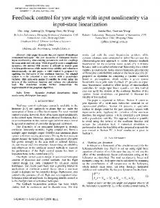
(b) Fig. 1. Block diagram.
For the WPT systems, the rectifier is the key opponent
(a) Conventional series diode rectifier.
(b) The proposed two-way rectifier.
to improve the RF-to-dc power conversion efficiency
(peE).
Different kinds of topologies are employed to
In this paper, a new rectifier topology is proposed to
peE
realize the rectifier, for instance, diode in series [2], diode
achieve high
in shunt [3], diodes in bridge [4], diodes in voltage
The proposed rectifier is based on the unequal power
doubler [5], and so on. However, as mentioned in [6],
divider and two sub-rectifying circuits which provide the
most of those rectifiers suffer a narrow input power range
peE
in which the RF-to-dc
is satisfied. It means that the
efficiency falls down very quickly at other input power
maximum
peEs
peE
over an extended input power range.
at different input levels. Thus, two peak
can be obtained and the high
peE
region can be
extended. Meanwhile, at the same input power levels, the
levels. This becomes a key limitation for the wireless
proposed rectifier can maintain nearly the same or even
charging applications in which the input power level could
higher
change significantly as the transmission distance varies.
levels. The rectifier is implemented and the simulated and
This
experimental results are presented for comparison.
reduces
transmission.
the
stability
Hence
a
and
speed
reconfigurable
of or
the an
power
wide
input
power
range.
However,
it
introduces
relatively complicated add-on switch components and detector circuits.
than the single one except at several power
adaptive
rectifier in [6] [7] was designed to harvest RF power over a
peE
II. RECTIFIER DESIGN Fig. l(a) shows the block diagram of the conventional series diode rectifier circuit, which is comprised of the matching network
that
maximizes the power transfer
,
80 /
75
I
, 65 , �
�
60
'-L.l
�
55
." '1
I
70
I
70
60
I
� �
I I
I, ,
I
II o
10
I
V
'\ l'-..
50
'-L.l
I
I
�[\
I ·
�
,
I
!
45 40
, .�
,
50
80
,
I
,, .i
,
,I
20
, - -
,
_.-
Rectifier I with 1000 n Rectifier [] with 300 n
" 30
40
50
60
70
�
30
20
80
)V
\1/ � 17 1\
o
5
10
15
20
25
30
Fig. 4.
power levels with load of 1000 n.
Matching
DC Pass
Network
Filter
•
70
Fig. 3.
60
25
t-
0::
� 30
i'--.r--.... t35
40
45
50
55
35 60
�
50
'-L.l
--
:
�
RL
./� 1\ pl -r\. '" 1/ 'f, ....... I -.....g::: l"" \ / '"� '\ fl
40
30
V
L _____________' 20
Layout of the rectifier in the proposed design.
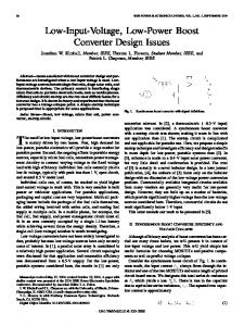
through the chain; the diode that rectifies the incoming RF signals; the DC pass filter which blocks the RF and higher harmonics introduced by the nonlinearity of the diode. With different loads as well as matching circuits, the rectifier obtains maximum RF-DC power conversion efficiency at different input power levels, as shown in Fig. 2. This kind of rectifiers obtains peak conversion efficiency only at certain input power level and the efficiency drops quickly at other input power levels [8]. To overcome this problem, we propose a novel topology as shown in Fig. l(b). It consists of an unequal power divider and two sub-rectifiers which are designed to achieve maximum conversion efficiencies at various input power levels. One sub-rectifier has the maximum conversion efficiency at a lower input power level and the other one at a high input power level. Using this method, the high conversion efficiency range can be extended. The topology of the two sub-rectifiers is the same as that in Fig. l(a) and the microstrip layout is shown in Fig. 3. It consists of a matching network, a capacitance, a packaged diode and a DC-pass filter. The matching network including a capacitance CI and the short stub is optimized to achieve high power transmission to the rectifier. For designing a high-efficiency rectifier, it is necessary to select a diode which has a low built-in voltage to operate at a low RF input power and has a high speed switching characteristics to follow a high frequency input signal.
10
15
20
f.
�
L3
__
(1)
Simulated return loss and PCE for various input
80
via
L2
_
?:l 2 3
15
Pin (mW)
maximum PCE at various input power levels.
W"t l
10
::;; V>
Fig. 2. The power conversion efficiency of single rectifier with
�cJI.!.iI"� �"III"C"2
-
�l--
20
'" I 1'-..
Pin (mW)
L,
I
!L--o
1�
40
v
o
10
20
30
40
50
60
70
25
?:l 2 3 (1)
to V> V>
30
0::
� 35
40 80
Pin (mW)
Simulated return loss and PCE for various input power levels with load of 300 Q.
Fig. 5.
Considering these requirements, the packaged Schottky diode of HSMS-2860 is adopted. The equivalent circuit parameters of a single diode are: VF=O.3V, Rs=6Q, Cjo=0.18pF and VB=7V, which are derived from the datasheet [9]. The DC- pass filter consists of a capacitance C2 for energy storage and smoothing the output signals, and three open stubs for suppressing the 2nd, 3rd, and 4th harmonics. The parameters of Li> L2, L3, and L4 are optimized to achieve high efficiency with the load RL. Since the highest efficiency is related to the input power and the load RL, the matching circuit (CI and LI) is optimized to achieve the high efficiency with different load resistance. The design procedures of the proposed rectifier are as follows. The first step is to design the sub-rectifying circuit with maximum PCE at a low input power level of 10 mW. The microstrip configuration of this sub-rectifier is shown in Fig. 3. The substrate has the thickness of 30mil, the dielectric constant of 2.55 and loss tangent of 0.0018. The load resistance is chosen as 1000 ohm. Following the design rules of rectifiers, the parameters are determined as: CI=1 pF, C2=100 pF, LI=37.4 mm, L2=56.1 mm, L3=28.4 mm, L4=14.4 mm. The simulated return loss
80
10
CO
� � 0 -l
E .a