A CHIP-SIZE ANTENNA FOR WIRELESS EEG J. H. Correia, N. S. Dias, C. A. Barbosa, P. M. Mendes University of Minho, Dept. Industrial Electronics, Campus Azurem, 4800-058 Guimaraes, Portugal
[email protected] Abstract ⎯ This paper presents the design and characterization of a patch antenna built on lossy substrates compatible with integrated circuits fabrication. Two different substrates were used for antenna implementation: highresistivity silicon (HRS) and Corning Pyrex #7740 glass. The antenna prototypes were built to operate close to the 5 GHz ISM band where applications like HIPERLAN and IEEE802.11a are standardized. They operate at a center frequency of 5.705 GHz (HRS) and 5.995 GHz (Pyrex). The application is a wireless wearable electroencephalogram (EEG) braincap. Wireless EEG allows patients to wear the braincap and maintain their mobility while simultaneously having their electrical brain activity monitored. Key Words: integrated antenna ,wireless EEG
I
INTRODUCTION
An emerging field is the wireless monitoring of human-body information. Body area network (BAN) comprises smart sensors able to communicate wirelessly to a base station. An wireless electroencephalogram (EEG) will provide a breakthrough in the monitoring, diagnostics and treatment of patients with neural diseases as epilepsy [1]. A wireless EEG microsystem will be composed by the neural electrodes (non-invasive and distributed in a braincap), electronics and a RF transceiver with an integrated antenna.
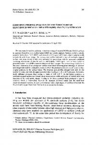
Figure 1. Classic EEG braincap with 32 Ag/AgCl electrodes and respective wires.
Usually the antenna component is placed outside the main chip due to well known constraints. First
and most important of all, the antenna tends to consume a lot of chip area. Different types of antennas have been suggested as candidates to be integrated within a single chip [2-5]. A patch antenna was developed because of its inherent advantages: low profile, light weight, low volume, low fabrication cost, possibility of linear and circular polarizations with simple feed, possibility for dual-frequency and dual-polarization, easiness to be integrated with microwave integrated circuits, feed lines and matching networks can be fabricated simultaneously with the antenna structure. Notwithstanding these advantages, usually they provide small bandwidth, low efficiency, and for standard design, relatively large area consumption. However, with the new standards for wireless communications operating at higher frequencies, chip size antennas become a topic of interest due to its size reduction. If the frequency is sufficiently high we can even think in some MEMS antenna. Those kinds of antennas may have the ability to tune the operating polarization or to shape its radiating beam in a preferable direction. Besides the size reduction due to the frequency increase, the provided bandwidth becomes also acceptable both for data communications and sensor applications. Due to the small range operation, the usually low gain provided by these antennas is supposed to be enough. Since the antennas should be integrated/embedded, the fabrication steps must include only materials and techniques compatible with the standard foundry processes. The standard processing steps found in a foundry fit quite well the need to fabricate a standard patch antenna. The main challenge is the material to be used as substrate. Parameters like substrate thickness, dielectric permittivity, dielectric losses, metal conductivity and thickness, should be evaluated to understand its influence on overall antenna performance.
362
II
ANTENNA DESIGN
fr =
II.1 TECHNOLOGY CONSTRAINTS
To be a good radiator, the antenna should be built on a substrate with low dielectric constant and losses. Also the metal patch should not contribute to the overall losses. The substrate thickness should not be thick to avoid surface wave excitation, but should not be thin to keep the bandwidth within acceptable values. The two types of substrate we have investigated for antenna design were the high resistivity silicon and Corning #7740 Pyrex glass. For simulations we have considered HRS with a dielectric permitivity, εr = 11.7 and a conductivity σ = 0.02 S/m – 0.05 S/m. For Pyrex wafer it was considered εr = 4.6, and a loss tangent of 0.5% (values known @ 1 MHz). The wafers thicknesses were 525 µm ± 25 µm for HRS and 500 µm for glass. To decrease the substrate losses when using HRS, a 300-nm layer of thermal silicon dioxide was used. This layer has an εr = 3.9 and is assumed as an insulator. Finally, the metalization layers were realized using a 2 µm layer of aluminium. Another possibility considered is to use copper to decrease metal losses. All these parameters are summarized on the following Fig. 2 2 µm Aluminium 300 nm SiO2 HRS εr= 11.7 σ = .05S/m 525 µm
2 µm Aluminium 500 µm
Pyrex εr= 4.6 tgδ = .005
Figure 2. Cross-section showing the materials used for antenna fabrication.
II.2 ANTENNA MODELING
With the technological constraints in mind, the first step was to find the shape dimensions of our patch antenna. A close value for the antenna length, L, is known to be half wavelength in the substrate. A first better value can be found using the equations from the transmission line model (TLM) approximation [5]. In this way we have for the dominant TM mode the resonant frequency:
1 2( L + ∆L) ε reff
(1)
µ 0ε 0
where L is the length of the antenna, ε0 and µ0 are the free space dielectric permitivity and permeability, εreff is the effective dielectric permitivity:
ε reff =
ε r +1 ε r −1 ⎡ 2
+
2
h⎤ ⎢⎣1 + 12 W ⎥⎦
−1 2
(2)
where εr and h are the relative dielectric permitivity and thickness of the substrate, and W is the width of the patch. Because of fringing effects the antenna looks larger than its physical dimensions. ∆L takes this effect in account. In order to facilitate its characterization, the antenna was designed to have a 50 Ω input impedance. The input impedance of the antenna can be adapted by choosing the right position for the feeding point [5]. Its value is maximum at the patch border and decreases as we move inside according to:
π
Z in = Z max cos 2 ( y ) L
(3)
where Zmax is the impedance at y = 0. Because the antenna was to be feed with a microstrip, the connection to a point inside the metal patch requires the use of wire bonding or an inset. The model was first built in Momentum ADS taking the values given by TLM approximation. The first step was to find the dimensions of the inset that provides the match to a 50 Ω microstrip line. Despite ADS Momentum simulator (a 2.5D simulator) ability to account for multilayer geometries it assumes the dielectric layers as being infinite. However, the finite size of the ground plane and substrate affect the antenna behavior and the 3D High Frequency Structure Simulator (HFSS) was used to include those effects. Picking the dimensions obtained with ADS Momentum we built a 3 dimensional model of the patch antenna as shown in Fig. 3.
363
The 8510C vector network analyzer was used to measure the return loss. The measured values for the antenna using HRS substrate are plotted against the simulated data on Fig. 5. We can see that the simulated data agrees quite well with the measured. The obtained operating frequency was near to 5.705 GHZ and the -10 dB return loss bandwidth was 90 MHz. W
0 -5 Return Loss [dB]
L
w0 w1 y0
Table 1. Dimensions of the patch antenna. L W y0 w0 w1
HRS 7.7 mm 7.6 mm 3.1 mm 0.36 mm 0.32 mm
Pyrex 11.7 mm 12.4 mm 4.7 mm .8 mm .05 mm
The prototype was fabricated at Delft Institute of Microelectronics and Submicron Technology, TUDelft.
-15 -20 -25 Measured Simulated
-30 -35
Figure 3. Meshed model of the HFSS patch antenna and layout with dimensions.
The next table shows the dimensions of the antenna for both kinds of used substrates.
-10
-40 5.6 5.625 5.65 5.675 5.7 5.725 5.75 5.775 5.8 Frequency [GHz]
Figure 5. Measured and simulated return loss for the antenna using HRS as substrate.
The return loss of the antenna on glass was also measured. For that antenna the measured operating frequency is 5.995 GHz and the –10 dB return loss bandwidth is 100 MHz. The DUCAT anechoic chamber facility at IRCTRTUDelft was used to measure the far field gain patterns. The results are plotted on Fig. 6. o
III MEASUREMENT AND ANALYSIS
o
-30
0 0 dB -5
o
30
-10 -15
The antenna characterization requires the placement of a SMA connector on the back of the microstrip antenna, as shown on Fig. 4. The surface of the aluminum metal patch was activated by means of electroless Ni deposition to allow soldering with the SMA connector.
-20
o
-60
o
60
-25 -30 -35 -40 -45
o
o
-90
90
-45 -40
-35 -30 -25
o
-120
o
120
-20 -15 -10
o
-150
-5 0 dB
o
180
Measured copolar H-Plane Measured o crosspolar Measured copolar E-plane Simulated copolar E-plane Simulated copolar H-plane
150
Figure 6. Measured gain patterns at 5.705 GHz for the antenna on HRS substrate.
Figure 4. The fabricated HRS patch antenna.
We can see that measured values are again in good agreement with simulated ones. As it was expected, the antenna exhibits a linear polarization
364
characteristic and the power is mainly radiated to the topside of the antenna. Nevertheless, it would be desirable a smaller power level at the back of the antenna. This drawback results from the small size of the ground plane. The maximum gain obtained was around 0.3 dBi. This small gain is essentially due to low efficiency, since the substrate is highly lossy. The gain for the antenna on glass was ~3 dBi. The gain increase is mainly due to a higher efficiency of the antenna. The final experiment was the signal transmition and reception using two of the fabricated antennas on HRS. The radiating antenna was connected to a signal generator and the receptor antenna to the spectrum analyzer. They where placed around 1 meter apart and the output power set to 0 dBm. A signal power of -50 dBm was received. This result is in agreement with all the other measured characteristics. The free space attenuation of a microwave signal can be described by: ⎛ 4π l ⎞ A=⎜ ⎟ ⎝ λ ⎠
2
were tested for antenna substrate. The microstrip patch antenna fabricated on HRS has area of 8 mm2 and operates at 5.705 GHz with approximately 90 MHz of bandwidth and a gain of 0.3 dBi. The microstrip patch antenna fabricated on Pyrex has area of 12 mm2 and operates at 5.995 GHz with approximately 100 MHz of bandwidth and a gain of 3 dBi. These characteristics fulfill the requirements for short-range communications for using the 5 GHz ISM band. The antennas fabricated on Pyrex substrate have, despite their larger size, better performance (efficiency up to 40%) when compared to antennas on HRS substrate. Currently, we are fabricating the low-power and low-voltage 5.7 GHz RF transceiver in 0.18 µm CMOS process. The final goal is improving the EEG medical diagnostics and therapy by using devices which reduce healthcare costs while at the same time preserving the mobility and lifestyle of patients.
(4)
V
where l is the propagation distance and λ is the wavelength. If we use the last equation with all the previously measured we can easily conclude that they all agree. To check the material tolerances we performed some simulations to check the influence of the substrate thickness and resistivity tolerance, and we changed also the oxide thickness. It can be seen that varying the substrate thickness from 500 µm to 550 µm and oxide thickness from 1 µm to 10 µm the operating frequency changed from around 5.7 GHz to 5.85 GHz. Changing the substrate conductivity from σ = 0.02 S/m – 0.05 S/m we found that efficiency changes from 19.6 % to 30.1 %.
IV CONCLUSIONS Antenna fabrication using the available standard fabrication processes used in IC fabrication was verified. This shows possibility of antenna integration with circuitry. A 3D model was built and used to accurately predict the antenna input and output characteristics. Two different materials
ACKNOWLEDGEMENTS
The authors would like to thanks the Portuguese Foundation for Science and Technology for funding this project (SFRH/BD/4717/2001 and POCTI / ESE / 38468 / 2001), M. Hajian and J. Zijderveld, from IRCTR-TUDelft, for their helpful support in far field pattern measurements. REFERENCES [1] IMEC press releases, “Ambulatory EEG”, Human ++ EU project, pp.1-2, 2003. [2] B.A. Floyd, Hung Chih-Ming; K.K O, “Intra-chip wireless interconnect for clock distribution implemented with integrated antennas, receivers, and transmitters”, IEEE J. of Solid-State Circuits, Vol. 37, Nº 5, pp. 543– 552, May 2002. [3] Zhang, Y.P., “Integration of microstrip patch antenna on ceramic ball grid array package”, Electronics Letters , Vol. 38 Nº 5, pp. 207 –208, February 2002. [4] Jun Zhao; S Raman, “An integrated chip-scale active antenna for 5-6 ghz wireless Microsystems”, RAWCON 2002, pp. 149–152, 2002. [5] Garg, R., Bhartia, P., Bahl, I., Ittipiboon, A., Microstrip Antenna Design Handbook, Artech House, 2001.
365