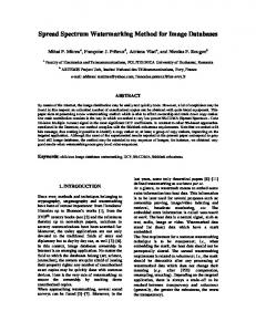
CTYPTOGRAPHIC TRUE RANDOM NUMBER GENERATOR FOR EMBEDDED NIOS PROCESSOR∗ Miloš Drutarovský, Martin Šimka Department of Electronics and Multimedia Communications, Technical University of Košice, Park Komenského 13, 04120 Košice, Slovak Republic E-mail:
[email protected]
Abstract The paper presents an implementation of a custom extension of commercially available NIOS processor embedded into Altera reconfigurable hardware. Added true random number generator uses recently proposed principle based on reconfigurable on-chip analog PLLs that are embedded in all modern Altera devices. Proposed solution significantly improves security of System on a Programmable Chip (SOPC) embedded cryptographic applications based on the NIOS processor. 1 Introduction Almost all cryptographic protocols require generation and use of secret values that must be unknown to attackers [1]. For example, True Random Number Generators (TRNGs) are required to generate public/private keypairs for asymmetric (public key) algorithms including RSA, DSA and Diffie-Hellman. Keys for symmetric and hybrid cryptosystems are also generated randomly. Unfortunately standard processors (including synthesisizable NIOS processor from Altera) are not able to generate true random numbers, as they are deterministic systems. Numerical pseudo-random generators relay on complexity and their standalone use in cryptography, for example to generate keys is inadvisable. The only way to get true random numbers, hence true security for crypto-systems, is to build a generator based on a random physical phenomenon. Current modern high-density Field Programmable Logic Devices (FPLDs) provide an alternative hardware platform even for system-level integration of embedded symmetric and asymmetric cryptographic algorithms but not for high quality TRNGs. Most hardware TRNGs follow unpredictable natural processes, such as thermal (resistance or shoot) noise or nuclear decay. Such TRNGs are not compatible with modern FPLDs and cannot provide a SOPC solution. This paper describes custom TRNG implementation based on recently proposed method [2] that uses on-chip analog PLLs included in Altera APEX FPLDs [3]. Proposed method reliably extracts intrinsic randomness from low-jitter clock signals synthesized by on-chip APEX analog PLLs. The TRNG is developed as an Intellectual Property (IP) building block optimized for NIOS processor and provides significantly higher system level security for complete embedded cryptographic SOPC designs. 2 NIOS Processor Overview The NIOS CPU [4] is a pipelined general-purpose RISC microprocessor that is generated by proprieatary Altera VHDL generator (SOPC Builder) and can be synthetized in all recent Altera FPLDs. NIOS supports both 32-bit and 16-bit architectural variants and both 16 and 32-bit variants use 16-bit instructions. The principal features of the NIOS instruction set architecture are: Large, windowed register file – NIOS implementations can include up to 512 internal general-purpose registers. The compiler uses the internal registers to accelerate subroutine calls and local variable access. Simple, complete instruction set – Both 32-bit and 16-bit NIOS variants use 16-bit wide instructions. 16-bit instructions reduce code size and instruction-memory badwidth. Powerful addressing modes – The NIOS instruction set includes Load and Store instructions that the compiler uses to accelerate structure access and local-variable (stack) access. ∗
This work was supported by VEGA grant 1/8130/01 – Digital Signal Processing and Watermarking in Multimedia Communications.
Extensibility – Users can incorporate custom logic directly into the NIOS arithmetic logic unit. The automatically-generated Software Development Kit (SDK) includes macros for accessing custom instruction hardware for C and assembly-language programs. Existing NIOS peripherals (e.g. UART, Timer, ...) as well as new custom peripherals can by connected through an Avalon bus. Avalon is a simple bus architecture designed for connecting onchip processor(s) and peripheral together into a SOPC. The principal features of the Avalon bus are: Simplicity – Provide an easy to understand protocol with a short learning curve. Optimized resource utilization – Conserve Logic Elements (LEs) inside the FPLD. Synchronous operation – Integrate well with other user logic that coexists on the same FPLD, while avoiding complex timing analysis issues. The structure of an example SOPC with user-defined custom TRNG, part of which is automatically generated by the SOPC Builder, is shown in Fig.1. User logic area
PCI_ctrl
Signals to off-chip devices
PCI bridge
PCI_addr PCI_data
Nios CPU
Data Instr
Off-chip memory
Avalon Bus Module
System Module PIO
Signals to on-chip user logic
Custom TRNG
Custom peripheral
Altera FPLD
Fig.1Example of a system module integrated with the custom TRNG into an Altera FPLD 3 Basic Principle of Implemented TRNG Modern Altera FPLDs use reconfigurable analog on-chip PLLs to increase performance and to provide on-chip clock-frequency synthesis. The basic principle behind our method is to extract the randomness from the jitter of the clock signal synthesized in the embedded analog PLL and is illustrated in Fig.2 [2]. CLK
PLL
CLJ
D
Q
q(nTCLK)
CLK
XOR Decimator (by KD)
x(nTQ)
Fig.2 Basic principle of randomness extraction from low-jitter clock signal The jitter is detected by the sampling of a reference clock signal ( CLK ) using related clock signal ( CLJ ) synthesized in the PLL. Let CLK be a system clock frequency with the frequency FCLK and an on-chip synthesized signal CLJ with the frequency
FCLJ = FCLK
KM KD
(1)
Let values of multiplication factor K M and division factor K D be relative primes, so
GCD ( K M , K D ) = 1
(2)
where GCD is an abbreviation of Greatest Common Divisor. Equation (2) ensures that the maximum guaranteed distance between the closest edges of CLK and CLJ (denoted as MAX ( ∆Tmin ) ) over the period TQ = K DTCLK = K M TCLJ
(3)
is equal to [2]
MAX ( ∆Tmin ) = TCLK
GCD ( 2 K M , K D ) 4KM
= TCLJ
GCD ( 2 K M , K D )
(4)
4K D
By proper choosing of K M , K D and TCLK it is possible to guarantee that MAX ( ∆Tmin ) < σ jit , where σ jit is the RMS value of PLL intrinsic jitter. According to [5], [6] an intrinsic jitter can be approximated by Gaussian distribution and σ jit ≥ 15 ps . Moreover proposed method is insensitive to an overall jitter characteristic as far as an intrinsic PLL jitter is included. Uniform distribution of generated true random bits with the period TQ (3) is guaranteed by using of moulo-2 (XOR) decimation of several independent signals from the synthesized delay-line [2]. 4 Hardware Mapping to the Altera FPLD To measure the real performance of our proposed TRNG, an Altera NIOS development board was selected. This development board was chosen to eliminate concerns about proper board layout technique. The same board was also used in [6] for reference PLL measurements so we can expect that jitter characteristics presented in [6] can be directly applied to our design. The board features a PLLcapable APEX EP20K200-2X with four on-chip analog PLLs. In order to use as large output data rate as possible, the two on-chip PLLs shown in Fig.3 were used for generating CLJ and CLK signals.
4 Dedicated Clocks 4.616 MHz
PLL4 clk1 inclk clk0
FEXT = 33.3 MHz
PLL2 clk1 inclk clk0
G4 G2 G1 G3
FEXT
80*14 = 33.570 MHz 11*101 :3
14 FEXT 14
= 33.3 MHz
14 FEXT 101
= 4.616 MHz
CLJ
CLK
Fig.3 Actual PLL configuration used in proposed TRNG IP block The external clock source was FEXT = 33.3MHz , on-chip synthesized clocks were FCLK = 33.3MHz (this is also the system clock frequency of NIOS processor) and FCLJ = FCLK (1120 / 3333) ≈ 33.6 MHz (can be modified according to other requrements). According to (4) these parameters ensure that MAX ( ∆Tmin ) ≈ 6.7 ps < σ jit . The output bit-rate of TRNG is 1/ TQ ≈ 10000 bits/s . The TRNG is written as parameterized VHDL code using standard Altera megafunction for embedded PLL configuration and LPM_ADD_SUB (adder/subtract) megafunction. TRNG peripheral can be accessed from the NIOS processor through the Data (read only) and Control/Status registers (write/read access) mapped into 2 memory locations shown in Fig.4. The TRNG can be accessed by standard memory pooling as well as by using an interrupt service request that can be enabled by an application program. Exact position of TRNG_base address and TRNG_IRQ can be configured by the SOPC Builder.
write access
read access 15 ...
TRNG_base+0
V =1/0 - valid/invalid data
2 1 0
TRNG Data (data register)
TRNG_base+1 X X X ... X X X C V (status register)
C =1/0 - proper/improper clocks 15 ...
2 1 0
X X X ... X X X (control register)
IE
IE=1/0 - interrupt enable/disable X
- undefined
Fig.4 Data and Control/Status registers of 16-bit TRNG Example of resource requirements of 16-bit and 32-bit NIOS with corresponding 16-bit and 32bit TRNG implementations are shown in Tab.1 (LE - Logic Element is the basic building block of Altera FPLDs). Presented results have been obtained by using Altera Quartus II ver.2.2, Altera NIOS 2.2 and Leonardo Spectrum v2001_1d.45. Tab.1 Results of mapping to Altera APEX EP20K200-2X Block LEs % of total capacity NIOS-16 / NIOS-32 1140/1480 14 / 18 UART 170 2 TRNG-16 / TRNG-32 150/200 2 / 2.5 ALL + interface logic 1669/2143 20 / 26 5 Statistical Testing of TRNG Output Data There are some well-documented general statistical tests that can be used to look for deviations from an ideal TRNG. It seems that NIST statistical test suite [7] is currently the most comprehensive publicly available test package. Our NIST statistical tests were performed on 1-Gigabit of continuous TRNG output acquired from the experimental hardware and followed testing strategy, general recommendations and result interpretation described in [7]. We used set of m = 1024 1-Megabit sequences produced by the TRNG and we have evaluated the set of P-values at a significance level α = 0.01 with similar results as in [2]. 6 Conclusion and Future Development The paper demonstrates the possibility to develop custom TRNG hardware for cryptographic applications in a digital FPLD. Advancements in FPLDs provide new option for design engineers. FPLDs maintain the advantages of custom functionality, like an ASIC, but avoid high development costs and the inability to make design modifications after productions. The fact that TRNG can be implemented inside the FPLD represents significant security and system advantage in embedded cryptographic applications. Future development of proposed TRNG IP block will include implementation of on-line TRNG hardware tests based on FIPS and AIS cryptographic standards.
References
[1]
[2] [3] [4] [5] [6] [7]
J.A. Menezes, P.C. Oorschot, S.A. Vanstone, “Handbook of Applied Cryptography”, CRC Press, New York, 1997. V. Fischer, M. Drutarovský, “True Random Number Generator Embedded in Reconfigurable Hardware”, Proceedings of the Workshop on Cryptographic Hardware and Embedded Systems CHES’2002, Redwood Shores, California, USA, August 2002, pp.415-430. APEX 20K Programmable Logic Device Family. Data Sheet, February 2002, ver. 4.3, 1--116, http://www.altera.com. NIOS 2.2 CPU. Data Sheet, September 2002, ver. 1.3, 1-14, http://www.altera.com/nios. “Jitter comparison analysis: APEX 20KE PLL vs. Virtex-E DLL“, Technical Brief 70, January 2001, ver.1.1, pp.1-7, http://www.altera.com. Superior Jitter management with DLLs. Virtex Tech Topic VTT013(v1.2), January 21, 2002, 1--6, http://www.xilinx.com. A. Rukhin, J. Soto, J. Nechvatal, M. Smid, E. Barker, S. Leigh, M. Levenson, M. Vangel, D. Banks, A. Heckert, J. Dray, S. Vo, “A statistical test suite for random and pseudorandom number generators for cryptographic applications“, NIST Special Publication 800-22, May 15, 2001, pp.1153, http://cs-www.ncsl.nist.gov/rng.