Low Complexity All-Optical Network Coder Architecture Eric D. Manley Department of Mathematics and Computer Science Drake University 2505 University Ave Des Moines, Iowa 50311, USA Email:
[email protected]
Abstract—Network coding, a networking paradigm in which different pieces of data are coded together at various points along a transmission, has been proposed for providing a number of benefits to networks including increased throughput, robustness, and security. For optical networks, the potential for using network coding to provide survivability is especially noteworthy as it may be possible to allow for the ultra-fast recovery time of dedicated protection schemes with the bandwidth efficiency of shared protection schemes. However, the need to perform computations at intermediate nodes along the optical route leads to the undesirable necessity of either electronically buffering and processing the data at intermediate nodes or outfitting the network with complex photonic circuits capable of performing the computations entirely within the optical domain. In this paper, we take the latter approach but attempt to mitigate the impact of the device complexity by proposing a low-complexity, all-optical network coder architecture. Our design provides easily scalable, powerful digital network coding capabilities at the optical layer, and we show that existing network coding algorithms can be adjusted to accommodate it.
I. I NTRODUCTION Network coding is a networking paradigm in which intermediate nodes in a network code together data from different input channels before transmitting on outgoing channels. Since it was introduced by Ahlswede et al. [1], network-codingbased strategies have been proposed for increasing network throughput, robustness, and security. The potential of realizing these benefits in optical networks, especially for optical protection has recently become an active area of research. Kamal et al. proposed network-coding schemes for survivable optical networks [2], [3], [4] in which electronic network coding operations supported the optical protection schemes. Menendez and Gannet [5] proposed performing the coding operations for survivability at the optical layer using alloptical XOR logic gates, and Hisano et al. [6] and An et al. [7] recently demonstrated network coding functionality using all-optical XOR logic gates. We investigated optical switch and optical network coder architectures which would provide unrestricted digital network coding capabilities at the optical layer [8], and Liu et al. applied an asynchronous network coding strategy at the optical layer [9]. In this paper, we propose a new design for a low-complexity, all-optical network coder device for providing digital network coding capabilities. The proposed design relies on optical XOR
technologies, tunable optical delays (TODs), and small optical switching components; and it scales to accommodate long codes through longer optical delays. In order to achieve this low complexity, we place restrictions on the network codes, but we show that existing network coding algorithms can be adjusted to accommodate the restrictions and still provide the same network coding benefits. In the next section, we motivate the problem by showing how network coding can be beneficial for optical network survivability. In Section III, we discuss some of the research into the component technology which could be used in our coding architecture, and then we propose our design in Section IV. In Section V, we discuss the necessary adjustments to network coding algorithms, and finally, we conclude in Section VI. II. N ETWORK C ODING AND O PTICAL N ETWORK S URVIVABILITY Given the tremendous bandwidth available on a given optical fiber, the impact of a network failure such as a fiber cut or switch failure is especially costly. For this reason, there has been much research into finding ways to allow networks to recover from faults quickly with as little overhead as possible. A. Dedicated and Shared Protection One straightforward approach to optical survivability is to simply send a redundant-copy along a second physicallydisjoint route. If a failure occurs on the primary route, then the message is still received on the backup route. This results in high connection availability and, if the propagation delay difference between the primary and backup routes is small enough, leads to very fast recovery. This kind of protection, however, is very expensive as it at least doubles the cost of deploying a connection. To cut down on this cost, the backup routes can be shared among several different potential failure scenarios [10]. For instance, consider the network in Figure 1(a), in which we have two connections to destination node d from sources s1 and s2 respectively. The two primary routes are shown with a heavy, red line and labeled with their data streams, a and b. The backup routes are shown with dashed, blue lines and labeled a0 and b0 to denote contingency routes for their respective streams. Note that the portion of the backup route from q to d is shared by both connections. Since both
1046
s2 s2
s2 b
b b
b
0
b
b0 a0
a0
q
s1
p s1
a0 , b0 b
a
q
a
p
s1
s3
a0 , b0
a+b
b
a
b
a
d (a) shared
p
q
c
d d
(a) shared
(b) network coded
s2
Fig. 1. Examples of two forms of protection
b
b
connections cannot use it simultaneously, neither connection transmits along it unless there is a failure along a primary route. In the event of a failure on link (s2 , p), b would be transmitted over hs2 , q, di without having to take the time to compute a new route. Likewise, if there were a failure along a’s primary route, then link (q, d) would be used in a’s recovery. This method has the benefit of saving on bandwidth, but it comes at the cost of a delay in the reestablishing of the connections due to the time it takes to discover the error, reconfigure the switch at q, and propagate along the entire backup route. With network coding, we can further improve on this example. Note that in Figure 1(b), s1 and s2 transmit redundant copies of their data along both the primary and backup routes simultaneously. However, at node q, the messages are added together (with arithmetic done over a finite number field to preserve message size) and transmitted over link (q, d). Thus node d receives a, a + b, and b. In the event that any one of these incoming messages is disrupted, d can still recover both a and b from the remaining two (e.g. by computing (a+b)−a to recover b). Like the dedicated protection example, there is very little delay in recovering the message after a failure as the redundant copies are sent at the same time as the originals. However, we also have the benefit of the lower bandwidth usage like we get with the shared protection example. B. Static Network Coding In general, the coded messages which are constructed and transmitted from intermediate nodes along a network route are linear combinations of the incoming messages at that node. Koetter and Medard presented an algebraic model for network codes which are robust against network failures, referring to them as static network codes [11]. For a single (possibly multicast) connection, they found that if a network coding solution exists for a particular connection after a set of potential failure scenarios taken individually, then a static network coding solution exists which is simultaneously robust against each of the failure scenarios. Unfortunately, this result does not generalize to network codes over multiple connections like the one shown in Figure 1(b). However, network coding approaches for special cases do exist. In a series of papers, Kamal et al. introduced 1 + N protection in which one may
a
q
p
a+b
b+c
c
s1
s3 a
c d (b) network coded
Fig. 2. Three-source protection example
contain network coded backup messages for N connections [2], [3], [4]. Network coding also provides us with opportunities for bandwidth savings that simple shared protection does not. Suppose we add an additional source, s3 , transmitting data stream c to our example as shown in Figure 2(a). In order to protect this connection by provisioning backup bandwidth (say, along the route hs3 , p, di), we would need a second wavelength on link (p, d). If such a channel is not available, then this connection would be blocked. However, if we employ network coding like the example shown in Figure 2(b), we use less bandwidth than needed in the shared protection example but without the delayed failure recovery. Note that in this case, d receives a, a + b, b + c, and c which are sufficient to recover all of a, b, and c from any three should one of the streams be disrupted. For example, with (a + b), (b + c), and c, we can recover b from (b + c) − c and a from (a + b) − (b + c) + c. Note that in this case, the bare symbol b is not sent on an uncoded channel but is nonetheless recoverable before or after a single failure. Thus, distinguishing between primary and backup routes may not be the best approach. For connections sharing a common destination, such a static network code exists whenever for any subset of the connections of size k there exists k + 1 link-disjoint paths between the sources and the destination [12]. The disadvantage to these approaches in an optical network is that coding operations must be supported at intermediate nodes. This can be accomplished by converting the optical signal to an electronic symbol, performing the operations using normal electronic computations, and then converting the result back into an optical signal for retransmission. This constant
1047
optical-electical-optical conversion and stopping/buffering of the flow is undesirable, and so the use of all-optical XOR gates for coding operations has been explored [5], [6], [7]. Using only XOR gates, however, limits coding operations to simple addition whereas most networking coding applications also require at least some scalar multiplication in the computing of a linear combination. To the best of our knowledge, our previous work in [8] is the only architecture which has been proposed to allow for full digital linear network coding at the optical layer, but its hardware complexity is fairly high, requiring O(m) optical XOR gates, TODs, and switching components (in order to support m-bit coded symbols). In order to make such a device more scalable, we present a lowcomplexity architecture which will allow for the benefits of full linear network coding while requiring only a small, constant number of XORs, TODs, and switching components while scaling up with longer delays. III. E NABLING T ECHNOLOGIES Our proposed all-optical network coder architecture relies on small optical switching components, TODs, and optical XOR gates. These devices are the subject of much current research, and in this section, we discuss of sample of recent laboratory demonstrations for these components with a variety of underlying technologies, keying techniques, etc. In practice, choosing a compatible selection of components is important to maintain a stable implementation. A. Switching Components Our architecture uses 1 × 2 and 2 × 2 all-optical switches. Researchers have demonstrated all-optical switches that are both fast and low power. Recently, much of this research has focused on the use of quantum dots for switching [13], [14].
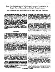
IV. D EVICE D ESIGN The design of our proposed all-optical network coder is shown in Figure 3. Note that these devices could be integrated into the fabric of the optical crossconnect or deployed in a shared bank of coders at some nodes. Data streams could then be routed to the coders as necessary by the crossconnect, and the output would be routed back into the input of the crossconnect for switching onto the appropriate outgoing channel. If more than two channels need to be coded together, multiple stages of coder devices need to be available in the bank, or the signals may need to be routed back through the switch and back into the shared bank an additional time. The device takes as input two symbols from F2m , the finite field of size 2m , encoded serially on the optical medium in m bits each. We denote these two bit patterns as a = am−1 am−2 . . . a0 and b = bm−1 bm−2 . . . b0 which we view as members of the polynomial representation of F2m , e.g., am−1 xm−1 + am−2 xm−2 + · · · + a0 . The coder will compute a linear combination ca ·a+cb ·b where the coding coefficients ca and cb are encoded in control signals in the multiplication stage of the device. After this scalar multiplication, the two products are added together in the addition stage, and then the result is normalized in the third stage of the device. We will describe each of these stages in more detail in this section. We assume that before the two bit streams enter the coder, their bit streams are aligned so that corresponding bits in the m-bit symbol arrive at the same time. Additional TODs may be necessary for this. We assume that the non-selected output of each 1 × 2 switch carries “0” bits. Exactly how this is accomplished depends on the modulation format. With on-off keying, it would not require any adjustment, but with more advanced formats, these may need to be 2 × 2 switches with a constant stream of zeros (originating at the crossconnect itself) routed to one of the two inputs on each switch. A. Multiplication Stage
B. All-Optical XOR Logic Gates For a review of technologies and experimental demonstrations of all-optical XORs, see Ref. [15]. The application of this technology specifically to network coding has also recently been demonstrated with a Mach-Zehnder interferometer-based XOR gate [6] as well as using four-wave mixing in a semiconductor optical amplifier [7]. C. Tunable Optical Delays The delays in our proposed architecture must be tunable in the sense that they can be adjusted to varying delay durations in order to line up appropriate bits for addition by the XOR gates. So, they must be able to adjust to all necessary data rates, and some need to be tunable for a discrete scalar multiple. Among the recent demonstrations of optical delays include those based on slow light in a Raman assisted fiber optical parametric amplifier sufficient for 10+ Gbit/s data rates [16] and another demonstrated at 416 Gbit/s for eight simultaneous signals using an optical-tapped delay line [17].
Our design restricts coding coefficients to the form 0xm−1 + 0xm−2 + · · · + 0xk+1 + 1xk + 0xk−1 + · · · + 0x + 0 so that multiplication can be performed with a simple bit shift (the impact of this restriction on the coding algorithms will be discussed in Section V). This shifting of k bits for some 0 ≤ k ≤ m−1 is accomplished using TODs which delay the signal by kτ where τ is the bit separation on the optical medium. Note that in the diagram for the multiplication stage in Figure 3, there are two such TODs labeled with ca and two with cb . These are the coefficient that each of the two inputs are multiplied by and thus are encoded on the control signals for the TODs. The reason that there are two for each coefficient is because the product of two degree m − 1 polynomials may have degree 2m − 2, and so the corresponding bit pattern takes 2m − 1 bits to represent. Thus, we need extra space on the medium until the normalization stage, and we split the multiplication work over two sets of TODs. The input symbols are alternated between the two sets using two 1 × 2 optical switches which are controlled with a mτ clock since a new symbol arrives every mτ time units. Note that each set
1048
multiplication 1x2 switch 1x2 switch
addition
TOD ca
normalization
optical XOR
TOD cb TOD ca
optical XOR
TOD cb
2x2 switch
TOD m TOD 1
optical XOR
optical XOR
optical splitter
Fig. 3. Optical Network Coder Architecture
of TODs effectively has 2m bits of space to work with for each symbol, so there will always be one bit of unused space after each symbol leaves the multiplication stage which will be important for the normalization stage. Additionally, we could allow for one or both of the coefficients to be the zero polynomial if the switches have the ability to drop the signal. B. Addition Stage Addition in F2m with our polynomial representation is accomplished via a simple XOR of the bit patterns, so following the multiplication stage, the two products ca a and cb b go through an all-optical XOR gate which results in the output d = ca a + cb b. Note that d is 2m − 1 bits long. C. Normalization Stage Normalization in the polynomial representation of F2m is accomplished by taking its modulus by an irreducible degree m polynomial. Any irreducible degree m polynomial will work for this step, and our architecture uses xm + x + 1. The choices of m for which this is irreducible are many and densely distributed [18], so the choice of this polynomial does not greatly restrict the symbol sizes compatible with the proposed device. However, using xm + x + 1 allows us to use the Itoh-Tsijii algorithm [19] to perform normalization very efficiently using two shifts and two additions (i.e. XORs) as we proposed in [8]. To see this, note that since xm mod xm + x + 1 = x + 1, for all xm+j with j ≥ 0 we have xm+j = xj+1 + xj mod xm + x + 1 = x + 1. So, d2m−2 x2m−2 + d2m−3 x2m−3 + · · · + dm+1 xm+1 + dm xm + dm−1 xm−1 + · · · + d0
d2m−2 d2m−3 d2m−4 · · · dm+1 dm d2m−2 d2m−3 · · · dm+2 dm+1 dm ⊕ dm−1 dm−2 dm−3 · · · d2 d1 d0
(1)
This sum is just the lower-order m bits of the 2m − 1 bit pattern for d added to two copies of the higher-order m − 1 bits with one of the copies shifted left by one bit. To see how this sum results from this circuit, note that since the symbols alternate between the two sets of TODs every m bits, after coming out of the addition stage, the higher-order m − 1 bits (followed by a single 0 bit) from one of the XORs is aligned with the lower-order m bits of the other XOR. The 2 × 2 switch at the beginning of the normalization stage is controlled by a mτ clock (just like the 1 × 2 switches in the multiplication stage) so that the m−1 higher-order bits of each addition output are switched to the bottom switch output and the lower order m bits are switched to the top switch output. The lower-order bits are then delayed by m so that the lowerorder and higher-order bits for each symbol are aligned. The m − 1 higher order bits are then split into two copies with an optical splitter and one copy is delayed by one bit before summed together. The result is then summed with the m lowerorder bits to produce the sum shown in (1). Note that the TODs in the normalization stage always shift a fixed number of bits. Thus, they need only be tunable enough to select the right bit separation for a given data stream. If a fixed data rate were used, only a fixed length of fiber would be necessary to accomplish the appropriate shift. D. Complexity
= d2m−2 (xm−1 + xm−2 ) + d2m−3 (xm−2 + xm−3 ) + · · · + dm+1 (x2 + x) + dm (x + 1) +dm−1 xm−1 + dm−2 xm−2 + · · · + d0 =(d2m−2 + dm−1 )xm−1 + (d2m−2 + d2m−3 + dm−2 )xm−2 + · · · + (dm+1 + dm + d1 )x + (dm + d0 ) mod xm + x + 1 = x + 1. In other words, we need to perform the following an XOR of three bit patters as follows:
This proposed architecture has low complexity, requiring only three small switches, four optical XOR gates, a splitter, and six TODs. This is highly scalable as the number of switching components and the number of XORs need not be increased for larger symbols (symbol size, of course, may need to grow large depending on the coding algorithm, the number of nodes in the communication group, the number of data streams being coded together, etc.). The only limit placed on the symbol size by this design is from the four TODs in the multiplication stage which need to be able to delay the signal a discrete number of bits up to one
1049
full symbol length. In contrast, our previous approach required each input to be split m times, and each shifted by a different bit length before entering an m-bit XOR gate (requiring O(m) XOR gates, switching components, and TODs) [8]. Using a reducing polynomial other than xm + x + 1 would require additional terms in the analogous sum (1) requiring additional XORs and more complicated switching to line up the bits. And, our normalization stage is undoubtedly simpler than basing it on a more naive approach like the long division algorithm with multiple stages of shifting and XORing.
VI. C ONCLUSION We have proposed an all-optical network coder which scales well, requiring only an increase in the length of delays for larger symbol sizes. We also showed that network coding algorithms can be adjusted to accommodate the restrictions on coding coefficients. When deployed in an optical network, possibly through a bank of shared coders at various network cross-connects, powerful digital network coding capabilities can then be provided at the optical layer. R EFERENCES
V. C ODING A LGORITHM A DJUSTMENTS Coding algorithms normally select the coefficients like ca and cb without restriction from symbols in the entire field F2m . Thus, limiting coefficients to symbols represented with exactly one “1” bit in the polynomial representation requires alterations to the network coding algorithms. However, we can show that network codes adhering to this restriction exist following the same approaches used for unrestricted network coding (as in e.g. [20], [21]), but usually needing a larger field. To see this, consider a coding scheme in which a destination node receives coded symbols from r source processes on r or more incoming channels. The coding coefficients can be propagated through the network so that on each incoming channel, we can set up a linear equation in r variables. If we can solve these equations simultaneously, then we have recovered the original messages. The equations can be written in a matrix form, and if the coding coefficients were selected in such a way that the determinant of the matrix is nonzero, then a solution can be found. If we write the entries of the matrix in such a way that the coding coefficients are indeterminants, then the determinant of the matrix can be expressed as a polynomial with the indeterminant coding coefficients as variables. If the polynomial is nonzero for some selection of coding coefficients, then that assignment corresponds to a valid network code. Denoting t as the maximum degree of a variable in the polynomial (which is limited depending on the traffic scenario, e.g. t is less than the number of destinations for a single multicast), note that the polynomial has at most t roots for each variable. Thus, we choose coding coefficients from F2m such that m > t which gives us m different symbols with exactly one “1” bit, not all of which can then be roots. Therefore, there must exist a selection of symbols for the originally indeterminant coding coefficients which give a nonzero result yielding a valid network code. Deterministic or random network coding algorithms like those in [20], [21] can then be applied under the restricted coefficient selection criteria to get a valid code. E.g., a random coding scheme for a single multicast would be successful with probability (1 − 2tm )η (where η is the number of channels assigned random coefficients) [21], and under our restriction, t η the probability would be (1 − m ) . Thus, our device allows for codes with the same success probabilities by using a much larger m. But given that m only impacts the coder architecture in the length of the delays, this is a reasonable tradeoff.
[1] R. Ahlswede, N. Cai, S.-Y. Li, and R. Yeung, “Network information flow,” IEEE Trans. Inf. Theory, vol. 46, July 2000. [2] A. E. Kamal, “1+N protection in optical mesh networks using network coding on p-cycles,” in Proceedings of IEEE Globecom, 2006. [3] ——, “A generalized strategy for 1+N protection,” in Proceedings of the IEEE International Conference on Communications (ICC2008), 2008. [4] A. E. Kamal, A. Ramamoorthy, L. Long, and S. Li, “Overlay protection against link failures using network coding,” IEEE/ACM Trans. on Netw., vol. 19, no. 4, pp. 1071–1084, August 2011. [5] R. Menendez and J. Gannet, “Efficient, fault-tolerant all-optical multicast networks via network coding,” in Conference on Optical Fiber communication/National Fiber Optic Engineers Conference (OFC/NFOEC), February 2008, pp. 1–3. [6] D. Hisano, A. Maruta, and K.-i. Kitayama, “Demonstration of all-optical network coding by using soa-mzi based xor gates,” in National Fiber Optic Engineers Conference. Optical Society of America, 2013. [7] Y. An, F. Da Ros, and C. Peucheret, “All-optical network coding for dpsk signals,” in National Fiber Optic Engineers Conference. Optical Society of America, 2013. [8] E. D. Manley, J. S. Deogun, L. Xu, and D. R. Alexander, “All-optical network coding,” IEEE/OSA J. Opt. Commun. Netw., vol. 2, no. 4, pp. 175 – 191, April 2010. [9] Z. Liu, M. Li, L. Lu, C.-K. Chan, S.-C. Liew, and L.-K. Chen, “Optical physical-layer network coding,” IEEE Photon. Technol. Lett., vol. 24, no. 16, pp. 1424–1427, August 2012. [10] C. S. R. Murthy and M. Gurusamy, WDM optical networks: concepts, design, and algorithms. Prentice Hall PTR Englewood Cliffs, 2002. [11] R. Koetter and M. Medard, “An algebraic approach to network coding,” IEEE/ACM Trans. on Netw., vol. 11, no. 5, pp. 782–795, Oct. 2003. [12] O. M. Al-Kofahi and A. E. Kamal, “Survivability strategies in multihop wireless networks,” IEEE Trans. Wireless Commun., vol. 17, no. 5, pp. 71–80, 2010. [13] H. Nakamura, Y. Sugimoto, and K. Asakawa, “Ultra-fast photonic crystal/quantum dot all-optical switch for future photonic networks,” in Lasers and Electro-Optics, 2006 and 2006 Quantum Electronics and Laser Science Conference. CLEO/QELS 2006. Conference on. IEEE, 2006, pp. 1–2. [14] M. Bajcsy, A. Majumdar, D. Englund, and J. Vuˇckovi´c, “Ultra-low power all-optical switching with a single quantum dot in a photonic-crystal cavity,” in SPIE OPTO. International Society for Optics and Photonics, 2013, pp. 863 516–863 516. [15] M. Zhang, L. Wang, and P. Ye, “All optical XOR logic gates: technologies and experiment demonstrations,” IEEE Commun. Mag., vol. 43, no. 5, pp. S19–S24, May 2005. [16] D. Dahan and G. Eisenstein, “Tunable all optical delay via slow and fast light propagation in a raman assisted fiber optical parametric amplifier: a route to all optical buffering,” Optics Express, vol. 13, no. 16, pp. 6234–6249, 2005. [17] S. Khaleghi, M. R. Chitgarha, M. Ziyadi, W. Daab, A. MohajerinAriaei, D. Rogawski, J. Touch, M. Tur, C. Langrock, M. M. Fejer et al., “A tunable optical tapped-delay-line that simultaneously and independently processes multiple input wdm data signals,” in Optical Fiber Communication Conference. Optical Society of America, 2013. [18] A. Menezes, P. van Oorschot, and S. Vanstone, Handbook of Applied Cryptography. CRC Press, 1996. [19] T. Itoh and S. Tsujii, “A fast algorithm for computing multiplicative inverses in GF(2m ) using normal bases,” Inf. Comput., vol. 78, no. 3, pp. 171–177, 1988. [20] R. W. Yeung, Information theory and network coding. Springer, 2008. [21] T. Ho and D. S. Lun, Network Coding: An Introduction. New York, NY, USA: Cambridge University Press, 2008.
1050