Aug 21, 2009 - Low voltage operation is one of the most effective low power design ... In this paper, we investigate circuit design using the recently proposed.
Low Power Circuit Design Based on Heterojunction Tunneling Transistors (HETTs) Daeyeon Kim, Yoonmyung Lee, Jin Cai*, Isaac Lauer*, Leland Chang*, Steven J. Koester*, Dennis Sylvester, David Blaauw Electrical Engineering and Computer Science, University of Michigan, Ann Arbor, MI *IBM T.J. Watson Research Center, Yorktown Heights, NY
{daeyeonk, sori}@umich.edu, {jincai, ilauer, lelandc, skoester}@us.ibm.com, {dmcs, blaauw}@umich.edu ABSTRACT The theoretical lower limit of subthreshold swing in MOSFETs (60 mV/decade) significantly restricts low voltage operation since it results in a low ON to OFF current ratio at low supply voltages. This paper investigates extremely-low power circuits based on new Si/SiGe HEterojunction Tunneling Transistors (HETTs) that have subthreshold swing < 60 mV/decade. Device characteristics as determined through Technology Computer Aided Design (TCAD) tools are used to develop a Verilog-A device model to simulate and evaluate a range of HETT-based circuits. We show that a HETT-based ring oscillator (RO) shows a 9−19X reduction in dynamic power compared to a CMOS RO. We also explore two key differences between HETTs and traditional MOSFETs, namely asymmetric current flow and increased Miller capacitance, analyzing their effect on circuit behavior and proposing methods to address them. Finally, HETT characteristics have the most dramatic impact on SRAM operation and hence we propose a novel 7-transistor HETT-based SRAM cell topology to overcome, and take advantage of, the asymmetric current flow. This new HETT SRAM design achieves 7−37X reduction in leakage power compared to CMOS.
Categories and Subject Descriptors B.3.1 [Memory Structures]: Semiconductor Memories – Static Memory (SRAM); B.7.1 [Integrated Circuits]: Types and Design Styles – Advanced Technologies, Memory Technologies, VLSI (very large scale integration); B.8.0 [Performance and Reliability]: General
General Terms: Performance, Design, Reliability Keywords:
Low Power Applications, Tunneling Transistor, SRAM
Design
1. INTRODUCTION Low voltage operation is one of the most effective low power design techniques due to its quadratic dynamic energy savings. Recently, a number of works [1-4] have shown aggressive supply voltage reduction to near or below the threshold voltage (Vth) of MOSFET devices with considerable reduction in power consumption. However, this power improvement has come at the cost of operation speed (typically 0 (in an NHETT). Hence, HETTs can be thought to operate “uni-directionally”, passing logic values only in one direction, which has significant implications on logic and especially SRAM design. Our analysis shows that another effect is a large increase in gate-to-drain capacitance (i.e., Miller capacitance) in HETTs compared to MOSFETs. This excess Miller capacitance can cause undesirable artifacts in the switching behavior of HETTs that is not present in MOSFETs. These differences in device operation and characteristics require careful study to understand their circuit design implications. In this paper, we show that HETT-based logic circuits are capable of improving energy efficiency by 19X compared to CMOS when operated at a supply voltage of 0.23 V. We particularly study SRAM design which is most impacted by the novel characteristics of HETTs. We show that the unidirectional characteristic of HETTs can actually be exploited in SRAM design to enable a novel 7T robust SRAM cell. The remainder of this paper is organized as follows: First, we briefly discuss HETT device operation and highlight the differences between the physics of HETT and MOSFET operation. Second, we introduce our modeling method for HETTs to enable circuit simulation of these devices, and examine dynamic power reduction in standard circuits compared to a commercial bulk CMOS 45nm technology. Third, we discuss the impact of the unique characteristics of HETTs on circuit behavior and describe how to address these issues. Finally, we present the new HETT-based SRAM cell topology that takes advantage of the asymmetric current flow of HETTs and quantify robustness improvements and leakage power reductions compared with CMOS-based SRAM.
2. HETT DEVICE CHARACTERISTICS The 60 mV/decade subthreshold slope limitation of conventional MOSFETs arises due to the thermionic nature of the turn-on mechanism. Tunneling transistors do not suffer from this fundamental limitation, since the turn-on in these devices is not governed by thermionic emission over a barrier.
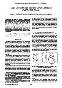
Drain Cgd Gate
Source Cgs
Ids Gate
Cgs
Cgd Source (a) NHETT
Figure 1. Tunneling FET device concept as depicted by a) band diagrams in the source-to-drain direction, and b) qualitative currentvoltage characteristics. Figure 1 illustrates the basic concept of tunneling transistor operation. In an n-type tunneling transistor, the source is doped p-type, the channel is undoped or lightly doped, and the drain is n-type. As shown in Figure 1, when the gate is biased positively the device is turned on because electrons in the valence band of the p-type source can tunnel into the conduction band of the channel. If the Fermi level in the source is less than a few thermal voltages (kT) below the valence band edge, the bandgap acts as an “energy filter”, precluding tunneling from the exponential portion of the Fermi-Dirac distribution. If the gate bias is reduced sufficiently so that the bottom of the conduction band in the channel rises above the top of the valence band in the source, the tunneling abruptly shuts off. Due to this filtering of the Fermi-Dirac distribution function by the bandgap, the subthreshold slopes can be significantly less than 60 mV/decade. A potential problem with tunneling transistors is that a very narrow bandgap semiconductor must be used to obtain sufficiently high ON current. However, narrow bandgap materials also lead to higher OFF currents, and are often incompatible with standard CMOS processing. To avoid this problem, a type-II hetero-junction tunneling transistor (HETT) can instead be employed. In such a case, the source-to-body contact has a staggered band lineup that creates an effective tunneling band gap, Egeff, which is smaller than that of the constituent materials. Such a band structure can also be realized in the Si/SiGe heterostructure material system, and complementary N- and P-HETTs can be fabricated, making this technology fully CMOS compatible. Figure 2 shows a schematic diagram of a complementary Si/SiGe HETT technology. For the circuit simulations in this work, an optimized device structure was used. The simulated HETT devices have a gate length of 40 nm, and a high-k gate dielectric with effective gate oxide thickness of 1.2 nm. For NHETT, the source consists of pure Ge, with 3% biaxial compressive strain, and Si channel with 1% biaxial tensile strain. The complementary PHETT design includes a strained Si source and pure Ge channel. Using
Ids
Drain (b) PHETT
Figure 3. Device symbols for (a) NHETT (b) PHETT. band offsets from [13], the effective bandgap for this structure is 0.22 eV. For the transport calculations, a non-local tunneling model [14] with a 2band dispersion relationship within the gap was used. Effective masses are 0.17m0 near the conduction band and 0.105m0 near the valence band in the silicon channel, and 0.10m0 near the conduction band and 0.055m0 near the valence band in the pure Ge source [15]. The device has a 2nm gate overlap of the source and an abrupt source doping profile. A gate work function of ~4.4eV is used to set the OFF current to