Session BD2 : "Numerical Techniques for Multi-Physics Electromagnetics" organized by Peter Russer
Multiphysics Modeling of Plasmonic Nanodevices Erping Li, Ping Bai, Iftikhar Ahmed and Hong Son Chu Department of Electronics and Photonics, A*STAR Institute of High Performance Computing, Singapore 13863
[email protected]
Abstract Plasmonic devices are modeled and simulated by incorporating a Lorentz-Drude model for the metallic materials and a multi-level multi-electron quantum model for the semiconductor materials into Maxwell’s equations. Some novel plasmonic devices such as a detector consisting of a dipole nanoantenna and a metal-semiconductor-metal detector, and a ring resonator based on a hybrid dielectric loaded waveguide are investigated with developed multiphysics modeling method. Simulation results show that the devices are very promising and can be combined with nanoelectronic integrated circuits to further improve their performance.
1. Introduction Plasmonics allows the manipulation of light at subwavelength scales. An unprecedented synergy could be reached by integrating plasmonic and electronic devices into the same platform by fully exploiting the advantages of plasmonics and nanoelectronics technologies [1,2]. For the integration of plasmonics and nanoelectronics platforms, a wide range of nanoscale plasmonic devices need to be developed, such as waveguide [3], modulators, filters [4] and detectors [5], whereas this development demands for new and further improvements in the existing computational electromagnetics techniques. The computational approach must be able to couple electromagnetics and electrons transport equations. In this paper, we incorporate the multi-level multi-electron quantum system approach into Maxwell’s equations for the simulation of the solid state part of a plasmonic structure, whereas for the simulation of the metallic part of a plasmonic structure, we incorporate a Lorentz-Drude (LD) model into Maxwell’s equations. For numerical analysis the finite-difference time-domain (FDTD) method is applied to the developed approach. The method is used to simulate a variety of plasmonics devices. As examples, a plasmonic detector and a ring resonator based on a hybrid dielectric loaded plasmonic waveguide are shown.
2. Multiphysics Modeling Methodology Electrons and photons are two fundamental elements in electro-optical systems and the interaction between them is a key mechanism in active photonics devices. We adopted the same principle for the modeling and simulation of plasmonics devices. The methodology is consisted of Lorentz-Drude and solid state media models. The Lorentz-Drude (LD) model is used to deal with intra-band (Drude model) and inter-band (Lorentz model) effects of metals, whereas the solid state media model deals with transient intra-band and inter-band electron dynamics, the carrier thermal equilibrium process in direct band gap semiconductors. In essence, the methodology consists of two parts, one for metals (LD model), and the other for semiconductors.
2.1 Model for metals At near infrared and optical frequencies, the relative permittivity of numerous metals becomes frequency dependent and can be described by a Lorentz-Drude (LD) model. For the Lorentz model different number of oscillators can be considered; for simplicity we considered only one oscillator. The permittivity dependent Maxwell equation with LD model is written as
∆ε Lω 2pL ω 2pD ∇ × H = jε 0ε ∞ωE + j ωE + j ωE j 2ω 2 + jΓD ω j 2ω 2 + jωΓL + ω L2 After using the auxiliary differential equation (ADE) approach equation (1) can be written as [6] ∇ × H = ε 0ε ∞
978-1-4244-6051-9/11/$26.00 ©2011 IEEE
ε ∂Q ∂E + JD + 0 L ∂t ∂t
(1)
(2)
Session BD2 : "Numerical Techniques for Multi-Physics Electromagnetics" organized by Peter Russer
ω 2pD ε 0 E = 2 ∆ε Lω pL E=
∂J D + J D ΓD ∂t
(3)
∂ 2 QL ∂QL + ΓL + ω L2QL 2 ∂t ∂t
(4)
where, equation (2) is Maxwell equation with both Drude “JD”and Lorentz “ model and equation (4) is for Lorentz model.
ε 0 ∂QL ∂t
” terms, equation (3) is for Drude
2.2 Model for Semiconductors In semiconductor medium, the electron dynamics is modeled by discretizing the conduction and valance bands into different energy levels. The occupation probability with respect to time for each level in the conduction and valance band, and the effect of carrier densities for different level pairs has been studied [7]. In our simulation ten energy levels are considered for both conduction and valance bands. From these levels we can calculate intra-band and inter-band transition times. It was observed that the electrons relaxation time to equilibrium is much slower in conduction band as compared to the valance band. For semiconductor model Maxwell equations can be expressed as in [6] ∇ × H = ε 0n2
∂E ∂P − ∂t ∂t
∇× E =−
∂B ∂t
(5)
where P is the macroscopic polarization density and represents total dipole moment per unit volume and can be expressed as [6]
(2ωah )2 U 2 A2 (r , t ) P (r , t ) d 2 Phk (r , t ) dPhk (r , t ) ω + Γ + + hk h ah kh k dt 2 dt h2 ( ) ( ) N r N r 2ω ah 2 dip − h dip − h U kh NVh (r , t ) − N Ch (r , t ) Ek ( r , t ) = 0 0 (r ) h N Ch NVh (r )
(6)
where k = x, y and z, Γh represent the de-phrasing rate at h th energy level after excitation, Ak is the vector potential, 2 3 ω ah is inter-band transition frequency, U kh = 3π ε 0c 3 ωah τ h , here is Planck’s constant ( ) divided by 2 π , c
is the speed of light in free space, ε 0 is permittivity of free space.
0 0 and N Ch are initial values of volume densities N Vh
of the energy states at level h in valance and conduction band respectively, while N Vh and N Ch are latter values. The Fermi-Dirac thermalization dynamics in the semiconductor is obtained by taking the ratio between upward and downward intra-band transitions for two neighboring energy levels. In this way thermalization effect, carrier densities and other effects can be incorporated in the formulations. After incorporation of the above effects into the polarization equation and then resulting equation into Maxwell’s equation, the discretized electric field equations for FDTD approach are written as [6] n +1
n
E x i + 1 , j ,k = E x i + 1 , j ,k + 2
2
−
1
M
Ey
1 i , j + ,k 2
Ez
n +1 i , j ,k +
n +1
∑P ε h =1
n +1
1 1 1 1 n+ n+ n+ n+ ∆t ∆t H z 12 1 − H z 12 1 + H z 12 1 − H z 12 1 i + , j − ,k i + , j ,k − ε∆y i + 2 , j + 2 ,k ε∆z i + 2 , j ,k + 2 2 2 2 2
h , x i + 1 , j ,k 2
n − Ph , x i + 1 , j ,k 2
1 1 1 1 n+ n+ n+ n+ ∆t ∆t H x 21 1 − H x 21 1 − H z 2 1 1 − H z 21 1 ε∆z i , j + ,k + i , j + ,k − ε∆x i , j + ,k + i , j + ,k − 2 2 2 2 2 2 2 2 n +1 n 1 M − ∑ Ph, y 1 − Ph , y 1 i , j + ,k i , j + ,k ε h =1 2 2
= Ey
1 2
n
1 i , j + ,k 2
+
1 1 1 1 n+ n+ n+ n+ ∆t ∆t 2 2 2 2 H H H H − − − y y x x 1 1 1 1 1 1 ε∆y 1 1 1 ε x ∆ i , j ,k + i + , j ,k + i − , j ,k + i , j + ,k + i , j − ,k + 2 2 2 2 2 2 2 2 2 n +1 n 1 M − ∑ Ph,z 1 − Ph ,z 1 i , j ,k + i , j ,k + ε h =1 2 2
= Ez
n
+
(7)
(8)
(9)
Session BD2 : "Numerical Techniques for Multi-Physics Electromagnetics" organized by Peter Russer In the case of semiconductor, the permittivity dependent electric field density is obtained by electron dynamics between conduction and valance bands, depending on Pauli exclusions principle, state filling effect and Fermi- Dirac thermalization. In the case of metal, the relative permittivity is dependent on resonance frequency and relaxation time of free and bounded electrons (Drude and Lorentz model). Consequently, there is difference in simulation approaches as in metals conduction and valance bands are overlapped while in the case of semiconductors they are separated due to band gap energy in between them.
3. Modeling Plasmonic Devices We explore the convergence of optics and electronics by using plasmonic waveguides for on-chip nanoscale optical data transmission, and have designed a number of plasmonic devices including waveguides [3], splitters, couplers, resonators and detectors [5] to optically transmit data between electronic devices; for example here we simulate a plasmonic detector and a ring resonator.
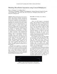
3.1 Plasmonic Detector The major challenge for the design of a nanoscale plasmonic detector is how to effectively couple the optical power from a plasmonic waveguide to a nanoscale active area in the detector. We propose a novel plasmonic detector structure by combining a dipole nanoantenna and a metal-semiconductor-metal (MSM) detector (Fig. 1a). The nanoantenna, formed by two metallic L-shaped nanorods and located at the end of a metal-insulator-metal (MIM) plasmonic waveguide, is used to receive plasmonic waves remotely [8]. The received plasmonic waves are localized in a nanocavity (Fig. 1b), formed between the two L-shaped nanorods, by exploiting the localized surface plasmon effects. By using the two L-shaped metallic nanorods as electrodes and filling the nanocavity with absorption materials, the nanoantenna becomes an MSM detector [5]. The highly concentrated optical power in the nanocavity excites electronhole pairs in the absorption material. The inset in Fig. 1c shows the photogeneration inside the nanocavity. The excited electrons and holes then drift to the two nanorods to form photocurrents under applied bias voltage (Fig. 1c). Simulation studies show that the optical power can be efficiently coupled from the plasmonic waveguide to the plasmonic detector. 28.8% of power from the end of the waveguide is absorbed by the absorption material in the nanocavity with a volume of 50×50×130nm3. The extremely small active area in the detector results sub-picosecond transit-time and atto-Farad internal capacitance, implying a potential THz-bandwidth.
3.2 Plasmonic Ring Resonator The other plasmonic component is a waveguide-based ring resonator. Its applications include optical (a)
(a)
(b)
Photocurrent (nA)
20
(b)
(c)
15
5
4
6.36
0
4.24
-20 -40 0
0 0
8.48
Ag
20
Y (nm)
10
(c)
1021
40
2.12
Ag 20
8
40
60
80 100 120
0.00
X (nm) 12
Bias voltage (mV)
16
20
Fig. 1 (a) Schematic of the plasmonic detector coupling to an MIM waveguide. (b) Power flow across the center of the detector in the xy-plane (c) Photocurrent of the detector vs bias voltage. Inset shows the photogeneration in the crosssection of the active area of the detector.
Fig. 2. (a) Schematic of a ring resonator built with a hybrid dielectric loaded waveguide. (b) Transmission of the resonator with a gap width of 250 nm and two sets of ring radii: R=2 & 5µm. (c) Near-field intensity distribution at 25nm above the silver film for the resonator with R=5µm at two different operating wavelengths: λ=1.55µm and λ=1.56 µm.
Session BD2 : "Numerical Techniques for Multi-Physics Electromagnetics" organized by Peter Russer switching, electro-optical switching, wavelength conversion, and filtering [4]. By taking the advantages of the hybrid dielectric loaded plasmonic waveguide (HDLW) [3], we build a HDLW-based ring resonator (HRR). It is formed by a ring waveguide placed in the proximity of a straight bus waveguide (Fig. 2a) to allow optical coupling between them. A portion of the optical power propagating in the straight waveguide (propagating mode) is coupled to the ring to excite a circulating mode, and the coupling depends on the gap separating the ring and the straight waveguide, and on the radius of the ring. The interference between the circulating mode and the propagating mode in the straight waveguide results in the filter characteristics of the HRR, which are characterized by the extinction ratio and the free spectral range. The extinction ratio of the HRR (defined as the ratio between minimum and maximum transmission outputs) is determined by the strength of coupling between the ring and the straight waveguide sections, and by the attenuation of the plasmonic wave propagation as well as the bend loss around the ring. On the other hand, the free spectral range and the HRR bandwidth are functions of the ring radius, the free-space wavelength and the effective mode index of the waveguide ring. As an example we show in Fig. 2b the transmission coefficient as a function of the wavelength for the optimal gap distance of 250 nm and two different ring radii R = 2 µm and 5 µm, respectively. It appears that the HRR has insertion loss less than 0.8 dB at R = 2 µm, and less than 1.1 dB at R = 5 µm. Very high extinction ratios (ER) are achieved, for example ER is 22 dB at R = 2 µm, and 20 dB at R = 5 µm. In addition, a large free spectral range of 22 nm and a bandwidth of 4 nm are obtained at the ring radius of 5 µm, which allow for accommodating 5 channels. The results show that our proposed structure (R~5 µm and input-output distance ~10 µm) achieves better optical performance than other counterparts [4,9] in terms of higher confinement, smaller free spectral range, narrower bandwidth and thus better quality factor, and higher extinction ratio as well as less total insertion loss. Furthermore, we sketch, in Fig. 2c, the near-field intensity to illustrate how the signal passing through the HRR with R = 5 µm can be switched on and off at different wavelengths.
4. Conclusions In summary, we have extended current techniques for computational electromagnetics by coupling them with the electronic transport equations. We incorporate the multi-level multi-electron quantum system approach and the LorentzDrude model into Maxwell’s equations to model the semiconductor and metallic materials for the plasmonic devices. The finite-difference time-domain method is applied to the derived formulations. A plasmonic detector is designed by combining a dipole nanoantenna and a metal-semiconductor-metal detector and a ring resonator is built based on a hybrid dielectric loaded plasmonic waveguide. Simulation results show that the developed plasmonic devices have potential for on-chip optical data transmission in the hybrid optics and electronics systems. Acknowledgments: This work is supported by Agency for Science Technology And Research(A*STAR), Singapore, SERC Research Grant, Metamaterials Programme: Nanoplasmon-ics. Grant No.:092 154 0098.
5. References
1. E. Ozbay, “Plasmonics: merging photonics and electronics at nanoscale dimensions”, Science, 311, 2006, pp. 189-193. 2. R. Zia, J. A. Schuller and M. L. Brongersma, “Plasmonics: the next chip-scale technology”, Mater. Today, 9, 2006, pp. 20–27. 3. H.S. Chu, E.P. Li, P. Bai and R. Hegde, “Optical performance of single-mode hybrid dielectric-loaded plasmonic waveguidebased components,” Appl. Phys. Lett. vol. 96, pp. 221103-221105, Jun 2010. 4. S. I. Bozhevolnyi, V. S. Volkov, E. Devaux, J.-Y. Laluet and T. W Ebbesen, “Channel plasmon subwavelength waveguide components including interferometers and ring resonators,” Nature, vol. 440, pp. 508-511, Jan 2006. 5. P. Bai, M. X. Gu, X. C. Wei and E. P. Li, “Electrical detection of plasmonic waves using an ultra-compact structure via a nanocavity”, Optics Express, Vol. 17, pp.24349-24357 (2009). 6. I. Ahmed, E. H. Khoo, O. Kurniawan and E. P. Li “Modeling and simulation of active plasmonics with the FDTD method by using solid state and Lorentz-Drude dispersive model” , Journal of Optical Society America B, Vol. 28, 2011, pp.352-359 7. Y. Huang, and S. T. Ho, “Computational model of solid state, molecular, or atomic media for FDTD simulation based on a multilevel multi-electron system governed by Pauli exclusion and Fermi-Dirac thermalization with application to semiconductor photonics,” Opt. Express 14 , 3569-3587, (2006). 8. M. X. Gu, P. Bai and E. P. Li, “Enhancing the reception of propagating surface plasmons using a nanoantenna”, IEEE Photonics Technol. Lett, 22, 2010, pp. 245-247. 9. T. Holmgaard, Z. Chen, S. I. Bozhevolnyi, L. Markey, and A. Dereux, “Dielectric-loaded plasmonic waveguide-ring resonators,” Optics Express, vol. 17, 2968-2975, Feb 2009.