POSFET Devices Based Arrays For Tactile Sensing Ravinder S. Dahiya1, Gaurav Kumar2, Giorgio Metta1,3, Maurizio Valle3, Leandro Lorenzelli4 1
RBCS, Italian Institute of Technology, Genoa, 16163, Italy 2 Indian Institute of Technology, Roorkee, 247667, India 3 University of Genova, Genova, 16145, Italy 4 Fondazione Bruno Kessler, Trento, 38050, Italy Email:
[email protected]
Abstract—This work presents and evaluates the novel POSFET (Piezoelectric Oxide Semiconductor Field Effect Transistor) devices based tactile sensing arrays - primarily developed for the robotic applications. The tactile sensing arrays, consisting of 5 x 5 POSFET touch sensing devices or taxels, are developed by spin coating and processing ~ 2.5 µm thick piezoelectric polymer P(VDF-TrFE) (Polyvinylidene Fluoride-Trifluoroethylene) film on the gate area of MOS devices. Each taxel on the array utilizes the change in polarization level (and hence change in the induced channel current), as a result of contact forces, to detect the contact events. Both the taxels and the array are designed to match spatio-temporal performance of the human fingertips. The POSFET tactile sensing arrays presented here are able to detect complex dynamic contact events such as rolling of an object over a surface.
I.
INTRODUCTION
Tactile sensing plays an important role in application domains like robotics, electrotextiles and medical prosthesis. In robotics the tactile information is needed during tasks like manipulation and exploration. The movement of robots from the structured environments to the daily life has also added new tasks such as safe robotic interaction in a humanpopulated environment. The way robots interact with the environment is an important issue, as real-world objects exhibit rich physical interaction behaviors - which depend on how heavy and hard the object is when hold, how its surface feels when touched, how it deforms on contact and how it moves when pushed. Such interaction behaviors can be better understood by touching or physically interacting with the objects – as humans do. Over the years, tactile sensing technology has improved and many force/pressure sensors and sensing arrays, using different materials and transduction methods e.g. Resistive/Piezoresistive, Quantum Tunneling, Capacitive, Optical, Magnetic, Piezoelectric etc. have been developed [3]. Most of these sensors are generally big in size and respond slow enough to detect only static and quasi-static contact events. However, real world contact events are generally dynamic in nature. The bigger size too makes many sensors unsuitable for body sites like robot‟s fingertips – which are involved in majority of the tasks. For fingertips large numbers (high density) of fast responding touch sensors are needed. For these reasons, miniaturized touch sensors using MEMS This work is supported in part by the European Commission Project ROBOSKIN (Grant No. ICT-FP7-231500) and in part by the Italian Ministry of Education University and Research under the project PRIN 2007 "Tactile Sensing System for Humanoid Robots using Piezo-polymer-FET devices".
approach have also been developed [4]. However, the inherent fragile nature of MEMS based touch sensor limits their usage to detection and measurement of contact forces that are at best equal to the lowest forces experienced by humans (see Table I) in a normal manipulative task. Mechanically flexible touch sensors, using organic FETs, have also been developed for large area skin type of applications [5]. However, best organics are known to have a mobility of about 1cm2/Vs versus 85 cm2/Vs for silicon based MOS devices [6], which limits their usage to recording of slow varying contact forces only. Moreover, the organic FET based touch sensors are too big to achieve the spatial acuity similar to that of humans‟ fingertips (see Table I). Nevertheless they are good enough to match spatial acuity of less sensitive parts (e.g. belly) of the human body. This work presents and evaluates the novel POSFET devices based tactile sensing arrays - primarily developed for the fingertips of humanoid robot ‘iCub’ [7]. The POSFET touch sensing used as taxels in these arrays show linear response over wide range of dynamic forces (tested in the range of 0.1-5 N with frequency up to 1 KHz) - which very well covers the range for forces experienced by humans in normal manipulative tasks (see Table I) [8]. The center-center distance of 1.5 mm between two adjacent taxels on the tactile arrays ensures human like spatial resolution and the taxel size (1mm x 1mm) ensures human like spatial acuity. Thus, the tactile sensing arrays can be used to measure dynamic contact events – distributed, both, in space and time. This has been demonstrated by reproducing the contact sequence from the taxels’ responses measured during rolling of a ring shaped probe on the surface of the array. This paper is organized as follows: The working of each POSFET taxel on the array is explained in section II. The design and fabrication steps of the tactile sensing arrays are presented in section III. The experimental evaluation of the tactile sensing array is presented in Section IV.
TABLE I.
KEY FEATURES FOR CUTANEOUS/TACTILE SENSE AT FINGERTIPS OF HUMANS [1, 2] Feature
Value
Receptor Density 100 in 1.0 x1.5 cm2 area. Range of Forces involved during normal 0.15-0.9 N manipulative tasks Detectable Frequency range of vibration DC-700 Hz Spatial Acuity Receptor level processing of contact data
1 mm Yes
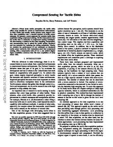
large area, which otherwise can be used for on chip electronics. Further, reliable interconnects between extended gate and MOS transistor is also an issue – more so in case of flexible touch sensing devices. The POSFET taxels used in this work are free from such problems. III. Figure 1. (left) The Structure and working of a POSFET taxel on the array. (right) The source-follower (with floating gate) connection scheme of each taxel on the array.
II.
WORKING OF POSFET TOUCH ELEMENTS
The metal – piezoelectric polymer – metal – insulator – semiconductor structure of a POSFET taxel, shown in Fig. 1, on the tactile sensing array is similar to a Metal-FerroelectricMetal-Insulator-Semiconductor FeRAM (Ferroelectric Random Access Memory). The fixed charges ±Q, shown in Fig. 1, appear due to the remanent polarization Pr of the piezoelectric polymer film and the charge neutrality condition. The charge carriers are thus accumulated at the surface of the semiconductor according to the polarization direction. For piezoelectric polymers in thickness mode, as in this work, the mechanical stress T3, electric field E3 and electric displacement D3 are related as [9]: 𝐷3 𝑑33 𝑇3 + ɛ33 𝐸3 Where, d33 and ɛ33 are the piezoelectric and dielectric constants of piezoelectric polymer respectively. Eq (1) shows that the electric displacement/charge and hence the polarization can be controlled by the electric field E3 and the applied force F or stress T3. While former is used in FeRAM to switch the polarization state, the later is used in the POSFET taxels to modulate the charge in induced channel of underlying MOS device [8]. Thus, the force variation is directly reflected into channel current of POSFET devices which can be further processed by an electronic circuitry that may be present on the same chip. Thus, each taxel is an integral “sensotronic” unit comprising of transducer and the transistor and is capable of „sensing and partially processing at same site‟. In this sense, a POSFET taxel can be compared with the mechanoreceptors in human skin - that not only sense the contact parameters, but also partially process the tactile data [2]. Such a marriage of sensing material and the electronics also helps in improving signal to noise ratio and hence the force sensitivity. Similar approach, but with extended gate, has been used in past for the development of ultrasonic [10] and touch sensors [11]. The extended gate approach brings the sensor and conditioning electronics closer and hence the overall response is better than that of conventional approach - in which, the sensor and conditioning electronics are placed at a distance. However the extended gates also introduce a large substrate capacitance, which in turn, significantly attenuates the charge/voltage available at gate terminals of MOS transistors and benefits offered by closely located sensor and electronics, are not fully exploited. The extended gates also occupy a
TACTILE SENSING ARRAY – DESIGN & FABRICATION
Like humans, the tactile sensing requirements are different for various parts of robot‟s body. For places like fingertips the tactile sensing arrays should have high spatio-temporal response – which requires many miniaturized sensors in a limited space. The 5 x 5 element tactile sensing arrays, shown in Fig. 2, are designed to have spatial resolution and acuity similar to that of human fingertips. The 1 mm x 1 mm size (fairly big when compared to the MOS devices obtained with present day technology) of each POSFET taxel ensures human like spatial acuity. The center-center distance of 1.5 mm between two adjacent taxels ensures human like spatial resolution. The MOS part of the POSFET taxel is obtained by using the n-MOS technological module of a non standard CMOS (Complementary MOS) technology, based on 4µm pwell ion sensitive FET (ISFET)/CMOS process. The MOS device part of the POSFET taxels is designed to have high aspect ratio (W=7500µm and L=12µm) - to obtain large transconductance. The fabrication step for developing the tactile sensing arrays are same as same as used for developing POSFET touch sensing devices [12]. However, the fabrication of tactile sensing arrays involves additional challenges such as depositing uniform polymer film over the array and simultaneous polarizing the polymer film (a step needed to orient the dipoles in the thickness direction and thus to obtain remanent polarization Pr) on all the taxels on the array. To deposit polymer film with uniform thickness a number of
experiments were performed on dummy silicon wafers (i.e. without any MOS device) [13]. The concentration of solution, spinner‟s speed and spinning time were used as variables in these experiments. A 10% P(VDF-TrFE) solution spin coated with 3000 rpm for 30 seconds resulted
Figure 2. (left) A part of the fabricated POSFET tactile sensing array before P(VDF-TrFE) polymer film deposition. The size of each taxel and the their separation are cleary marked. (right) SEM image of POSFET tactile sensing array after P(VDF-TrFE) polymer film deposition. Top metal of all taxel is connected to single pad.
Figure 4. The response of various taxels, when a probe is rolled over the diagonal taxels of the tactile sensing array. (top) The responses of individual taxels. Only responses of diagonal taxels and those adjacent to diagonal taxels are shown here. The instants showing the maximum response of the taxels are marked. The time from t1 to t8 (with left-right arrow) show the response of taxels when probe is rolled from taxel (5, 1) towards taxel (1, 5). Similarly t9 to t17 (with right-left arrow) depict the movement in opposite direction. (middle) Response of all taxels over 2.5 seconds measurement period. (bottom) 3D bar plots obtained from the individual responses of various taxels, when probe is rolled over the tactile sensing arrays from taxel taxel (5, 1) towards taxel (1, 5) and back. The direction of rolling is evident from the spatial and temporal response of the taxels on the array. Taxel (1,2) and (3,3) on the array are not working.
in a uniform (~ 1% variation across a 4 inch Si wafer) 2.5 µm thick polymer film and hence same is used in this work. The thickness of polymer film on various POSFET taxels was found to be uniform. The in situ poling is another
challenge due to the fact that a voltage of 250 volts is needed to polarize the 2.5 µm thick polymer film. Such high voltages might alter the MOS device characteristics. To avoid such an unpleasant situation measure like, a) short
grounding the substrate and all metal layers under polymer, and b) increasing the voltage in cumulative steps of 50 volts were adopted. However, even after these steps two taxels ((1, 2) and (3, 3)) on the array were found to be not working after poling step. To avoid such problems other poling methods too will be explored in future. IV.
RESULTS
Before putting the tactile sensing arrays on the fingertips of robot it is important to evaluate their capability of detecting dynamic contact events that are distributed, both, in space and time. In a number of experiments performed in past the POSFET devices were found to have linear response over wide range of dynamic forces (tested in the range of 0.1-5 N with frequency up to 1 KHz) [8]. The response of various taxels, connected in source-follower (floating gate) arrangement (see, Fig. 1) was found to be ~50mV/N. Similar response was observed from the POSFET taxels on the array. However, the aim of present experiment is to evaluate the performance of various taxels on the array for a real world like stimulus. In this context the results presented here are qualitative rather than quantitative. To match real world like stimulus the ring shaped probe, comprising of a 2 mm wide ball bearing, was manually rolled over the diagonal taxels of the array. The representative arrangement of the experiment is shown in Fig. 3. NI 6259 data acquisition board was used to acquire the response of various taxels. During experiments, the tactile sensing array was covered with a 200 µm protective PDMS film. The force applied on the probe during rolling was not controlled. However, it was maintained more or less constant. Similarly, the path followed by probe too was not controlled, but, was more or less maintained along the diagonal taxels. While diagonal taxels were fully covered by probe during rolling, the adjacent taxels were only partially covered. Effect of this can be noticed from the response of taxels shown in Fig. 4. The diagonal taxels have higher response then off-diagonal elements. The maximum response of the diagonal taxels is around 0.15 volts and that of adjacent taxels is less than half of this value. The minor output variation among the set of diagonal and set of taxels adjacent to diagonal taxels could be due to the fact the controlled force was not applied during rolling. The contact sequence reproduced from the taxels’ responses, shown in Fig. 4, clearly demonstrated the capability of tactile sensing arrays to detect dynamic contact events (distributed, both, in space and time). The time period of 0.41 sec for one rolling cycle (two times diagonal travel e.g. t1- t17, t2 - t18 etc.) observed in Fig. 4 is in good agreement with the actual travel time of 0.416 sec. A total of six such rolling cycles were completed in period of 2.5 seconds. Thus, the tactile sensing arrays presented here are capable of detecting the complex dynamic contact events like rolling.
Figure 3. (left)Test array on package. (right) The representative arrangement of the experiment. A thin ball bearing (~2 mm wide) was used as probe.
can also be used for detecting other contact events like slippage. A SOC/SIP approach can be very helpful for improving the real time dynamic contact events detection capability of the tactile sensing arrays. Realization of the arrays on flexible substrates can further improve their utility in robotics and other areas. REFERENCES [1]
[2]
[3]
[4]
[5]
[6]
[7] [8]
[9]
[10]
[11]
[12]
CONCLUSION Tactile sensing arrays presented in this work have spatiotemporal features similar to that of receptors in the human fingertip. The tactile sensing arrays are able to detect dynamic contact events that vary both in space and time. This capability has been demonstrated by way of rolling a ring probe on the surface of array. Thus, the tactile sensing arrays presented here
[13]
J. M. Wolfe, K. R. Kluender, D. M. Levi, L. M. Bartoshuk, R. S. Herz, R. L. Klatzky, and S. J. Lederman, Sensation and Perception. Sunderland, Massachusetts USA: Sinauer Associates Inc., 2006. R. S. Johannson and J. R. Flanagan, "Coding and use of tactile signals from the fingertips in object manipulation tasks," Nature Reviews Neuroscience, vol. 10, pp. 345-359, 2009. M. R. Cutkosky, R. D. Howe, and W. Provancher, "Force and Tactile Sensors," in Springer Handbook of Robotics, B. Siciliano and O. Khatib, Eds. Berlin Heidelberg: Springer 2008, pp. 455-476. H. Takao, K. Sawada, and M. Ishida, "Monolithic Silicon Smart Tactile Image Sensor With Integrated Strain Sensor Array on Pneumatically Swollen Single-Diaphragm Structure," IEEE Transactions on Electron Devices, vol. 53, pp. 1250-1259, 2006. T. Someya, T. Sekitani, S. Iba, Y. Kato, H. Kawaguchi, and T. Sakurai, " A Large-Area, Flexible Pressure Sensor Matrix with Organic FieldEffect Transistors for Artificial Skin Applications," Proc. National Acad. Sciences, vol. 101, pp. 9966-9970, 2004. D.-H. Kim, J.-H. Ahn, H.-S. Kim, K. J. Lee, T.-H. Kim, C.-J. Yu, R. G. Nuzzo, and J. A. Rogers, "Complementary Logic Gates and Ring Oscillators on Plastic Substrates by Use of Printed Ribbons of SingleCrystalline Silicon," IEEE Electron Dev. Lett., vol. 29, pp. 73-76, 2008. www.robotcub.org, "iCub," 2009. R. S. Dahiya, G. Metta, M. Valle, L. Lorenzelli, and A. Adami, "Piezoelectric Oxide Semiconductor Field Effect Transistor Touch Sensing Devices," App. Phy. Lett. vol. 95, pp. 034105 (1-3), 2009. R. S. Dahiya, M. Valle, and L. Lorenzelli, "SPICE Model of Lossy Piezoelectric Polymers," IEEE Transactions on Ultrasonics, Ferroelectrics and Frequency Control, vol. 56, pp. 387-396, 2009 R. G. Swartz and J. D. Plummer, "Integrated silicon-PVF2 acoustic transducer arrays," IEEE trans. on Electron Dev., vol. 26, pp. 1920-32, 1979. I. Graz, M. kaltenbrunner, C. Keplinger, R. Schwodiauer, and S. Bauer, "Flexible ferroelectret field-effect transitor for large-area sensor skins and microphones," App. Phy. Lett., vol. 89, pp. 073501(1-3), 2006. R. S. Dahiya, M. Valle, G. Metta, L. Lorenzelli, and A. Adami, "Design and Fabrication of POSFET Devices for Tactile Sensing " in TRANSDUCERS 2009, The 15th IEEE Int. Conf. on Solid-State Sensors, Actuators and Microsys., Denver, USA, 2009, pp. 1881-1884. R. S. Dahiya, M. Valle, L. Lorenzelli, G. Metta, and S. Pedrotti, "Deposition Processing and Characterization of PVDF-TrFE Thin Films for Sensing Applications," in IEEE Sensors 2008, Lecce, Italy, 2008, pp. 490-493.