Vol.30, No.2
Journal of Semiconductors
February 2009
Ternary logic circuit design based on single electron transistors Wu Gang(吴刚)† , Cai Li(蔡理), and Li Qin(李芹) (Institute of Science, Air Force Engineering University, Xi’an 710051, China) Abstract: Based on the I–V characteristics and the function of adjustable threshold voltage of a single electron transistor (SET), we design the basic ternary logic circuits, which have been simulated by SPICE and their power and transient characteristics have been extensively analyzed. The simulation results indicate that the proposed circuits exhibit a simpler structure, smaller signal delay and lower power. Key words: single electron transistor;adjustable threshold voltage;ternary logic DOI: 10.1088/1674-4926/30/2/025011 PACC: 7335C
1. Introduction The multi-value logic (MVL) circuit is an important part of modern digital electronics. MVL circuits allow more than two levels of logic, so we may have ternary, quaternary or more levels of logic styles. Compared with the conventional binary logic, the information density in MVL is much higher. MVL can reduce the number of operations that is necessary to implement a particular mathematical function; thus it has an advantage in terms of reduced area, which in turn reduces parasitics associated with routing and provides a higher speed of operation. In the design of a digital system, an e level system costs less. Because 3 is the nearest integer to e, the ternary logic circuit has attracted more attention[1−4] . Over the past 40 years, researchers have advanced the performance of circuits and reduced their power dissipation by reducing characteristic size. But the reduction of characteristic size leads to some problems such as metal inter-linkage and current tunnelling which can hamper the development of integrated circuit. The single electron transistor (SET) needs only one or several electrons to work, so it can work with ultimately low power dissipation. On the other hand, the much smaller size of the SET can advance the integration density. So the low power dissipation and high density make the SET a key element for further development of integrated circuits[5] . In this paper, we introduce the basic ternary logic circuits and analyze the characteristic of adjustable threshold voltage of SET. Also, we design the basic ternary gates and extensively analyze the power and the transient characteristics of the designed circuits.
2. Basic ternary logic circuits A kind of multi-value algebra system is necessary for the design of a multi-value logic circuit. In several actual multivalue algebra systems, the Disjoint algebra[6] is prevalent in engineering. The min (minimum) operator, max (maximum) operator and the literal operator are the basic operations in the Disjoint algebra.
Consider L = {0, 1, · · · , R − 1} is the set of the multivalue variable in the R value system. The max operator is defined as X, X > Y max(X, Y) = , (1) Y, X 6 Y where X, Y belong to the set R. The min operator is defined as X, X 6 Y , min(X, Y) = Y, X > Y where X, Y belong to the set R. The literal operator is defined as R − 1, X = a a a X = , 0, X , a
(2)
(3)
where X belongs to the set R. If there are two thresholds, the literal operator is defined as R − 1, a 6 X 6 b a b , (4) X = 0, X 6 a , X > b where X belongs to the set R.
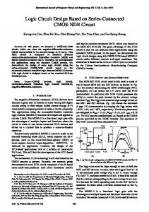
3. Characteristics of adjustable threshold voltage of SET The basic characteristics of SET are Coulomb oscillation and Coulomb block. Furthermore, SET can have multiple gates that give it an adjustable threshold voltage. The two-gate SET is shown in Fig.1, where Cg1 and Cg2 are the gate capacitances, and CD and CS are the tunnel junction capacitances. For the two gates, one gate is used as a voltage input port Vin and the other gate as a threshold voltage adjusting port Vcon . The current through the two tunnel junctions in series is controlled by the voltage on the island. On the basis of Ref.[7], the formula to calculate the island voltage is V island =
1 (CD VDS + Cg1 Vin + Cg2 Vcon − ne), CΣ
(5)
† Corresponding author. Email:
[email protected]
Received 2 August 2008, revised manuscript received 3 September 2008
025011-1
c 2009 Chinese Institute of Electronics ⃝
Wu Gang et al.
February 2009
Fig.1. Sketch of two-gates SET.
Fig.2. SET’s characteristic of controlled threshold.
where CΣ = Cg1 + Cg2 + CD + CS , and n is the number of the background charge that can be ignored. We consider the inherent threshold voltage from the quanta island to be Vth , which is related to the parameter C∑ [8] . The SET will turn on when Visland > Vth . Here Visland is
Visland =
1 (CD VDS + Cg1 Vin + Cg2 Vcon ) > Vth . CΣ
(6)
Then the apparent threshold voltage of the transistor from gate Vin is given as Vin >
CΣ V th − Cg2 Vcon − CD VDS . Cg1
(7)
So the threshold voltage for the gate Vin is Vth1 =
CΣ Vth − Cg2 Vcon − CD VDS . Cg1
(8)
From Eq.(8), we can see that the threshold voltage for Vin is controlled by Vcon . The characteristic of controlled threshold is shown in Fig.2.
4. Design of a ternary logic circuit based on an SET In this study, the Mahapatra-Ionescu-Banerjee (MIB) model[9] of SET is used. The MIB model is based on the “Orthodox theory of single electron tunneling”[6] , and it is a physically based compact model that can be used for single or multiple gates and symmetric or asymmetric devices. The model also accounts for the background charge and is valid in
Fig.3. Ternary complement gate.
a wide range of drain to source voltages | VDS | 6 3e/CΣ and temperature T 6 e2 /10 kBCΣ . In the ternary logic circuit based on SET, we will use two kinds of SET, i.e. SET1 and SET2. The parameters of SET1 and SET2 are: Cg1 = Cg2 = 0.01 aF, CD = CS = 1 aF, RD = RS =1 MΩ, Vcon1 = 8 V and Vcon2 = 4 V, where Vcon1 and Vcon2 are used to adjust the threshold voltages of SET1 and SET2 respectively. Based on these parameters, the threshold voltages of SET1 and SET2 are respectively 2.5 and 6.5 V. In order to reduce the leak current of the SET, Vin should be much larger than VDD . So the voltage of the ternary logic level in input and output should be defined respectively. On the input, we define the logic “0” as a voltage less than Vth1 , the logic “1” as a voltage between Vth1 and Vth2 , and the logic “2” as a voltage greater than Vth2 . Because the supply voltage is 0.2 V, on the output, logic “0” would correspond to a voltage less than V1 (≈ 0.1 V), logic “1” to a voltage between V1 and V2 (≈ 0.2 V), and logic “2” to a voltage greater than V2 . 4.1. Ternary complement gate The ternary complement gate based on an SET is shown in Fig.3 (a). The circuit is composed of two resistances R and two SETs, i.e. SET1 and SET2. In order to realize the correct logic function, R should be much greater than the tunnel junction resistance, so we consider R = 400 MΩ. When Vin is less than Vth1 , both SETs are off. Hence, the output voltage is held at VDD . When Vin reaches a value between Vth1 and Vth2 ,
025011-2
J. Semicond. 30 (2)
Wu Gang et al.
Fig.4. Ternary max gate.
SET1 is on and SET2 is off. Hence, the output voltage is held approximately at VDD /2. When Vin exceeds Vth2 , SET2 turns on and SET1 turns off, so the output voltage is pulled down to almost 0. The output voltage can be expressed as VDD , Vin < Vth1 Vout = VDD /2, Vth1 6 Vin 6 Vth2 . 0, Vin > Vth2 Figure 3 (b) shows the DC transfer characteristic of the complement gate. 4.2. Max gate The max gate based on an SET is shown in Fig.4 (a). In the circuit, Vin1 and Vin2 are the inputs of the max gate, and Vout is the output of the max gate. When either Vin1 or Vin2 is logic “2”, either of two SETs turns on, so the output voltage Vout is VDD , that is logic “2”. When (Vin1 , Vin2 ) = (0, 1) or (Vin1 , Vin2 ) = (1, 0), the output voltage Vout should be logic “1”. Hence, V1 < VDD
R1 < V2 . R1 + R2
(9)
Fig.5. Ternary min gate.
Hence, the relation of R1 and R2 is R1 < R2 < 2R1 . In our simulation, R2 = 32 R1 has been chosen (R1 = 400 MΩ, R2 = 600 MΩ). Figure 4 (b) shows the DC transfer characteristics of the proposed max gate with Vin1 at logic “0” and Vin2 being swept from logic “0” to logic “2”. 4.3. Min gate The min gate based on an SET is shown in Fig.5 (a). In the circuit, Vin1 and Vin2 are the inputs of the min gate, and Vout is the output of the min gate. When either Vin1 or Vin2 is logic “0”, there is no access between VDD and the ground, so the output voltage Vout is 0, that is logic “0”. When (Vin1 , Vin2 ) = (2, 1) or (Vin1 , Vin2 ) = (1, 2), the output voltage Vout should be logic “1”. Hence,
When (Vin1 , Vin2 ) = (1, 1), the output voltage Vout should be logic “0”. Hence, V1 < VDD R
2
2
R1 + R1
< V2 .
(10)
V1 < VDD
(11)
(12)
When (Vin1 , Vin2 ) = (1, 1), the output voltage Vout should be logic “2”. Hence,
Considering V1 = 13 VDD and V2 = 23 VDD , Equation (10) can be simplified as 1 R1 < R2 < 2R1 , R1 < R2 < 4R1 . 2
R1 < V2 . R1 + R2
V1 < VDD
R1 < V2 . 2R2 + R1
(13)
Considering V1 = 13 VDD and V2 = 23 VDD , the above formulas can be simplified as
025011-3
Wu Gang et al.
February 2009
Fig.7. Ternary 1 X1 gate. Fig.6. Ternary 0 X0 gate.
1 1 R1 < R2 < 2R1 , R1 < R2 < R1 . 2 4
(14)
Hence, the relation of R1 and R2 is 12 R1 <R2 <R1 . In our simulation, R2 = 34 R1 has been chosen (R1 = 400 MΩ, R2 = 300 MΩ). Figure 5 (b) shows the DC transfer characteristics of the proposed max gate with Vin1 at logic “2” and Vin2 being swept from logic “0” to logic “2”. 4.4. Literal gate The 0 X0 gate based on SET is shown in Fig.6 (a). The circuit is composed of two SETs with a pull-up resistance. When the input Vin is logic “0”, both SETs are off, so output voltage Vout is VDD , that is logic “2”. When the input Vin is logic “1”, SET1 is on and SET2 is off, then there is an access between VDD and the ground, so the output voltage Vout is 0, that is logic “0”. When the input Vin is logic “2”, SET1 is off and SET2 is on, then there is an access between VDD and the ground, so the output voltage Vout is 0, that is logic “0”. Figure 6 (b) shows the DC transfer characteristics of the 0 X0 gate. The 1 X1 gate based on SET is shown in Fig.7 (a). The circuit is composed of on SET with a pull-down resistance. When the input Vin is logic “0” or “2”, SET1 is off, so output voltage Vout is 0, that is logic “0”. When the input Vin is logic “1”, SET1 is on. There is an access between VDD and the ground, so output voltage Vout is VDD , that is logic “2”. Figure 7 (b) shows the DC transfer characteristics of the 1 X1 gate.
The 2 X2 gate based on SET is shown in Fig.8 (a). The circuit is composed of a SET with a pull-down resistance. When the input Vin is logic “0” or “1”, SET2 is off, so output voltage Vout is 0, that is logic “0”. When the input Vin is logic “2”, SET2 is on. There is an access between VDD and the ground, so output voltage Vout is VDD , that is logic “2”. Figure 8 (b) shows the DC transfer characteristics of the 2 X2 gate. Based on the literal gates 0 X0 , 1 X1 and 2 X2 , we can design other kinds of literal gates[6] .
5. Analysis of a ternary logic circuit based on an SET The above ternary circuits have been simulated by SPICE. We can get the average delay time, average power and delay-power product. The performance parameters above are shown in Table 1. From Table 1, we can see that the average delay time of ternary logic circuits reaches the 10−11 s level, and the power reaches the nW level. The ternary circuits based on SET have much better transient performance and much lower power. In the design of the ternary logic circuits based on SET, the pull-up resistance and pull-down resistance have a more important effect on the performance of circuit. When the pull-up resistance or pull-down resistance increases, the delay time will increase but the power will decrease. So, when designing these circuits, we can adjust the pull-up resistance or pull-down resistance so as to make the delay-power product reach the minimum.
025011-4
J. Semicond. 30 (2)
Wu Gang et al. Table 1. Average delay, average power and delay-power product of the designed circuits.
x X0 1 1 X 2 2 X min max 0
Average delay (ns)
Average power (nW)
Delay-power product (10−18 J)
0.08 0.08 0.04 0.04 0.07 0.1
0.92 0.48 0.44 0.40 0.41 0.44
0.074 0.04 0.018 0.016 0.028 0.044
circuit, we must select an appropriate value of VDD to find a balance between noise margin and power dissipation.
6. Conclusion The SET has an adjustable threshold voltage. We can get SETs with different threshold voltages by different controlling voltages on the gate, which is advantageous for the SET in designing a multi-value logic circuit. The basic ternary logic circuits have been designed. The simulation results indicate that the ternary logic circuits have a simpler structure, much better transient and much lower power dissipation.
References Fig.8. Ternary 2 X2 gate.
The SET has particular characteristics different from the conventional MOS transistor, so there are problems to be discussed. (1) In order to avoid the leak current through SET, the voltage on gate Vin must be larger than the supply voltage VDD . Then the voltage level of the input is larger than the voltage level of the output, leading to poor driven ability. For this problem, we can use a CMOS amplifier to magnify the output voltage so as to drive the next circuit. (2) For the SET, in order to realize the characteristic of Coulomb block, the supply voltage VDD must be smaller, so the noise margin of the proposed circuits is smaller. In order to advance the noise margin, we must advance the supply voltage VDD and decrease the gate capacitance at the same time , but this will increase the power dissipation. So in the design of the
[1] Wang J S, Wu C Y, Tsai M K. Low power dynamic ternary logic. IEE Proc, 1988, 135(6): 221 [2] Wu X W. CMOS ternary logic circuit. IEE Proc, 1990, 137(1): 21 [3] Mateo D, Rubio A. Quasi-adiabatic ternary CMOS logic. Electron Lett, 1996, 32(2): 99 [4] Toto F, Saletti R. CMOS dynamic ternary circuit with full logic swing and zero-static power consumption. Electron Lett, 1998, 34(11): 1083 [5] Likharev K K. Single-electron devices and their applications. Proc IEEE 1998, 87(4): 602 [6] Epstein G. An equational axiomatization for the disjoint system of post algebras. IEEE Trans Comput, 1973, C-22 (4): 422 [7] Mahapatra S, Vaish V, Wasshuber C, et al. Analytical modeling of single electron transistor for hybrid CMOS-SET analog IC design. IEEE Trans Electron Devices, 2004, 51(11): 1772 [8] Shen Bo, Jiang Jianfei. Numerical analysis of amplifier based on SET. Chinese Journal of Semiconductors, 1997, 18(8): 626
025011-5