the given probabilities can be duplicated and whether there is free- dom to ... zeros and ones; they are processed by ordinary logic gates, such as. AND and OR.
The Synthesis of Combinational Logic to Generate Probabilities ∗
Weikang Qian, Marc D. Riedel, Kia Bazargan, and David J. Lilja Department of Electrical and Computer Engineering University of Minnesota, Twin Cities
{qianx030, mriedel, kia, lilja}@umn.edu ABSTRACT As CMOS devices are scaled down into the nanometer regime, concerns about reliability are mounting. Instead of viewing nanoscale characteristics as an impediment, technologies such as PCMOS exploit them as a source of randomness. The technology generates random numbers that are used in probabilistic algorithms. With the PCMOS approach, different voltage levels are used to generate different probability values. If many different probability values are required, this approach becomes prohibitively expensive. In this work, we demonstrate a novel technique for synthesizing logic that generates new probabilities from a given set of probabilities. Three different scenarios are considered in terms of whether the given probabilities can be duplicated and whether there is freedom to choose them. In the case that the given probabilities cannot be duplicated and are predetermined, we provide a solution that is FPGA-mappable. In the case that the given probabilities cannot be duplicated but can be freely chosen, we provide an optimal choice. In the case that the given probabilities can be duplicated and can be freely chosen, we demonstrate how to generate arbitrary decimal probabilities from small sets – a single probability or a pair of probabilities – through combinational logic.
1.
INTRODUCTION AND BACKGROUND
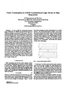
randomness. The technology generates random numbers that are used in probabilistic algorithms [6]. Vdd noise Vin CL
Figure 1: A PCMOS switch. It consists of an inverter with its input coupled to a noise source.
A PCMOS switch is an inverter with the input coupled to a noise source, as shown in Figure 1. With the input Vin set to 0 volts, the output of the inverter has a certain probability p (0 ≤ p ≤ 1) of being at logical one. Suppose that the probability density function of the noise voltage V is f (V ) and that the trip point of the inverter is Vdd /2, where Vdd is the supply voltage. Then, the probability that the output is one equals the probability that the input to the inverter is below Vdd /2, or Z Vdd /2 p= f (V ) dV.
It can be argued that the entire success of the semiconductor industry has been predicated on a single, fundamental abstraction, namely, that digital computation consists of a deterministic sequence of zeros and ones. From the logic level up, the precise Boolean functionality of a circuit is prescribed; it is up to the physical layer to produce voltage values that can be interpreted as the exact logical values that are called for. This abstraction delivers all the benefits of the digital paradigm: precision, modularity, extensibility. And yet, as circuits are scaled down into the nanometer regime, delivering the physical circuits underpinning the abstraction is increasingly costly and challenging. Power consumption is a major concern [1]. Also, soft errors caused by ionizing radiation are a problem, particularly for circuits operating in harsh environments [2]. We advocate a novel view for digital computation: instead of transforming definite inputs into definite outputs – say, Boolean, integer, or real values into the same – we design circuits that transform probability values into probability values; so, conceptually, real-valued probabilities are both the inputs and the outputs. The circuits process random bit streams; these are digital, consisting of zeros and ones; they are processed by ordinary logic gates, such as AND and OR. The inputs and outputs are encoded through the statistical distribution of the signals instead of specific values. When cast in terms of probabilities, the computation is robust [3]. The topic of computing probabilistically dates back to von Neumann [4]. Many flavors of probabilistic design have been proposed for circuit-level constructs. For instance, [5] presents a design methodology based on Markov random fields, geared toward nanotechnology. Recent work on probabilistic CMOS (PCMOS) is a promising approach. Instead of viewing variable circuit characteristics as an impediment, PCMOS exploits them as a source of
Thus, with a given noise distribution, p can be modulated by changing Vdd . In [7], PCMOS switches are applied to form a probabilistic systemon-a-chip (PSOC) architecture that is used to execute probabilistic algorithms. In essence, the PSOC architecture consists of a host processor that executes the deterministic part of the algorithm, and a coprocessor built with PCMOS switches that executes the probabilistic part of the algorithm. The PCMOS switches in the coprocessor are configured to realize the set of probabilities needed by the algorithm. This approach achieves an energy-performanceproduct improvement over conventional architectures for some probabilistic algorithms. However, as is pointed out in [7], a serious problem must be overcome before PCMOS can become a viable design strategy for many applications: since the probability p for each PCMOS switch is controlled by a specific voltage level, different voltage levels are required to generate different probability values. For an application that requires many different probability values, many voltage regulators are required; this is costly in terms of area as well as energy. This paper presents a synthesis strategy to mitigate this issue: we describe a method for transforming probability values from a small set to many different probability values entirely through combinational logic. For what follows, when we say “with probability p,” we mean “with a probability p of being at logical one.” When we say “a circuit,” we mean a combinational circuit built with logic gates.
∗ This work is supported by a grant from the Semiconductor Research Corporation’s Focus Center Research Program on Functional Engineered Nano-Architectonics, contract No. 2003-NT1107.
Example 1 Suppose that we have a set of probabilities S = {0.4, 0.5}. As illustrated in Figure 2, we can generate new probabilities from this set:
−∞
P(x = 1) = 0.4 x
P(z = 1) = 0.6 z
P(x = 1) = 0.4 P(z = 1) = 0.2 x z AND y
2.
• In an early set of papers, Gill discussed the problem of generating a new set of probabilities from a given set of probabilities [8, 9]. He focused on synthesizing a sequential state machine to generate the required probabilities.
P(y = 1) = 0.5 (b)
(a)
Figure 2: An illustration of generating new probabilities from a given set of probabilities through logic. (a): An inverter implementing pz = 1 − px . (b): An AND gate implementing pz = px · py .
• In recent work, the proponents of PCMOS discussed the problem of synthesizing combinational logic to generate probability values [7]. These authors suggest a tree-based circuit. Their objective is to realize a set of required probabilities with minimal additional logic. This is positioned as future work; no details are given.
1. An inverter with an input x with probability 0.4 will have output z with probability 0.6 since for an inverter, P (z = 1) = P (x = 0) = 1 − P (x = 1).
• Wilhelm and Bruck [10] proposed a general method for synthesizing switching circuits to achieve a desired probability. Their designs consist of relay switches that are open or closed with specified probabilities. They proposed an algorithm that generates circuits of optimal size for any binary fraction.
(1)
2. An AND gate with inputs x and y with independent probabilities 0.4 and 0.5, respectively, will have an output z with probability 0.2 since for an AND gate, P (z = 1) = P (x = 1, y = 1) = P (x = 1)P (y = 1).
(2)
Thus, using only combinational logic, we can get the additional set of probabilities {0.2, 0.6}. � Motivated by this example, we consider the problem of how to synthesize combinational logic to generate a required probability q from a given set of probabilities S = {p1 , p2 , . . . , pn }. We consider three scenarios: Scenario One: The probabilities in a set S are predetermined and each element of S can be used as the input probability no more than once. (We say that the probability is non-duplicable.) The problem is to construct a circuit that has input probabilities taken from S and produces an output probability q. Scenario Two: The probabilities in a set S can be freely chosen and each element in S can be used as the input probability no more than once. The problem is to find a good set S such that, for an arbitrary probability, we can construct a circuit to generate it. Scenario Three: The probabilities in a set S can be freely chosen and each element in S can be used as the input probability any number of times. (We say that the probability is duplicable.) The problem is to find a good set S such that, for an arbitrary probability, we can construct a circuit to generate it. Our contributions are: 1. We provide an FPGA-mappable solution to the problem in Scenario One. We transform the problem into a linear programming problem. 2. We prove an optimal choice of a set S for the problem in Scenario Two. Again, the solution is FPGA-mappable. 3. We provide a set S consisting of two elements that can be used to generate arbitrary decimal probabilities in Scenario Three. The proof is constructive: we show a procedure for synthesizing logic that generates such probabilities. 4. We provide a set S consisting of a single element that can be used to generate arbitrary decimal probabilities in Scenario Three. (This is essentially a mathematical result, since the probability value is not a simple value, but the root of a polynomial.) 5. Finally, we propose a practical algorithm based on fraction factorization, which optimizes the depth of the circuit that generates a decimal fraction in Scenario Three.
RELATED WORK
We point to three related pieces of research:
In contrast to Gill’s work and Wilhelm and Bruck’s work, we focus on combinational circuits built with logic gates. Our approach dovetails nicely with the circuit-level PCMOS constructs. It is complementary and orthogonal to the switch-based approach of Wilhelm and Bruck. Note that Wilhelm and Bruck assume that the probabilities in the given set S can be duplicated. We also consider the case where they cannot. Also, our scheme can generate arbitrary decimal probabilities, whereas the method of Wilhelm and Bruck only generates binary fractions.
3.
PROBLEM FORMULATION AND SOLUTION
As stated in Section 1, we consider three scenarios. These hinge on: 1. Whether the set S is given or can be freely chosen. 2. Whether the probabilities from S are duplicable. In all three scenarios, we assume that the probabilistic inputs are independent.
3.1
Scenario One: Set S is given and the elements are not duplicable.
The problem considered in this scenario is: given a set S = {p1 , p2 , . . . , pn } and a required probability q, construct a circuit that, given inputs with probabilities from S, produces an output with probability q. Each value of S can be utilized as an input probability no more than once. Although the assumption that each element of S can be utilized as an input probability only once might seem contrived, in fact, this constraint occurs if a circuit has a bounded number of inputs and each input is fixed at a specific probability. For instance, consider an n-input lookup table FPGA with each input having a predetermined probability. In this case, the set of predetermined input probabilities forms the set S with each element appearing in the circuit no more than once. With the assumption that the probabilities are non-duplicable, we are building a circuit with n inputs, the i-th input of which has probability pi . (If a probability is not utilized, then the corresponding input is just a dummy.) Our solution to this problem is based on the construction of a truth table for n variables. Each row of the truth table is annotated with the probability that the corresponding input combination occurs. Assume that the truth table has n variables x1 , x2 , . . . , xn and xi has probability pi . Then, the probability of the input combination x1 = a1 , x2 = a2 , . . . , xn = an (ai ∈ {0, 1}, for i = 1, . . . , n) is P (x1 = a1 , x2 = a2 , . . . , xn = an ) =
n Y i=1
P (xi = ai ).
A truth table for a two-input XOR gate is shown in Table 1. The fourth column is the probability that each input combination occurs. Here P (x = 1) = px and P (y = 1) = py . Table 1: A truth table for the XOR of two variables listing the probability that each input combination occurs. x y z Probability 0 0 0 (1 − px )(1 − py ) 0 1 1 (1 − px )py 1 0 1 px (1 − py ) 1 1 0 px py
The output probability is the sum of the probabilities of input combinations that produce an output of one. Mathematically, assume that the probability of the i-th input combination (corresponding to minterm mi ) is ri (0 ≤ i ≤ 2n − 1) and that the output of the circuit is zi (zi ∈ {0, 1}, 0 ≤ i ≤ 2n − 1). Then, the output probability is po =
n 2X −1
zi r i .
(3)
i=0
For the example in Table 1, the output probability is po = r1 + r2 = (1 − px )py + px (1 − py ). Thus, constructing a circuit with output probability q is the same problem as determining the zi ’s such that Equation (3) evaluates to q. In the general case, depending on the values of pi and q, it is possible that q cannot be exactly realized by any circuit. The problem then is to determine the zi ’s such that the difference between the value of Equation (3) and q is minimized. We can formulate this as the following optimization problem: ˛P n ˛ ˛ 2 −1 ˛ Find zi that minimizes ˛ i=0 zi r i − q ˛
(4)
such that zi ∈ {0, 1} for i = 0, 1, . . . , 2n − 1.
(5)
This optimization problem is a linear 0-1 programming problem that can be solved using standard techniques. A circuit implementing the solution can be synthesized readily. The solution is also applicable for use in an n-input lookup-table based FPGA architecture: the i-th input bit of the FPGA is just zi .
3.2
Scenario Two: Set S is not given and the elements are not duplicable
In Scenario One,˛ when solving the˛ optimization problem, the ˛P n ˛ minimal difference ˛ 2i=0−1 zi ri − q ˛ is actually a function of q, which we denote as h(q). That is, ˛2n −1 ˛ ˛X ˛ ˛ ˛ h(q) = min ˛ zi r i − q ˛ . ˛ ∀i,zi ∈{0,1} ˛
(6)
probability. A circuit with n inputs has a truth table consisting of n 2n rows. There are a total of 22 different truth tables for n inputs. For a given input probability assignment, each truth table can give n a distinct output probability. Thus, we can get at most 22 distinct probabilities for a set S of size n. Example 2 Consider the truth table shown in Table 2. Here, we assume that P (x = 1) = 4/5 and P (y = 1) = 2/3. The corresponding probability of each input combination is given in the fourth column. For different truth table output column assignments (z0 z1 z2 z3 ), we obtain different output probabilities. For example, if (z0 z1 z2 z3 ) = (1010), then the output probability is 5/15; if (z0 z1 z2 z3 ) = (1011), then the output probability is 13/15. There are 16 different assignments for (z0 z1 z2 z3 ) and so we can get a maximum of 16 different output probabilities. In this example, they are 0, 1/15, . . . , 14/15 and 1. �
Table 2: A probability truth table for two variables. The output column (z0 z1 z2 z3 ) has a total of 16 different assignments. x y z Probability 0 0 z0 1/15 0 1 z1 2/15 1 0 z2 4/15 1 1 z3 8/15 n
Let N = 22 . For a set S with n elements, call the N possible probability values b1 , b2 , . . . , bN and assume that they are arranged in increasing order. That is b1 ≤ b2 ≤ · · · ≤ bN . Note that if the output column of the truth table consists of all zeros, the output probability is 0. If it consists of all ones, the output probability is 1. Thus, we have b1 = 0 and bN = 1. The first question is: what is a lower bound for H(S)? We have the following theorem. Theorem 1 The lower bound for H(S) is
bi + bi+1 P ROOF. Note that for a q satisfying bi ≤ q ≤ , 2 bi + bi+1 h(q) = q − bi ; for a q satisfying < q ≤ bi+1 , h(q) = 2 bi+1 − q. Thus, Z 1 H(S) = h(q) dq 0 0 b +b 1 Z i i+1 Z bi+1 N −1 X 2 @ = (q − bi ) dq + b +b (bi+1 − q) dq A i=1
i=0
Assume that q is uniformly distributed on the unit interval. The mean of h(q) for q ∈ [0, 1] is solely determined by the set S; it gives the overall approximation error of S. We can see that the smaller the mean is, the better the set S is. Thus, the mean of h(q) is a good measure for the quality of S, which we denote as H(S). That is, Z 1 H(S) = h(q) dq. (7) 0
The problem considered in this scenario is: given an integer n, choose a set S of size n of values in the unit interval that produces a minimal H(S). Note that the only difference between Scenario One and Scenario Two is that in Scenario Two, we are able to choose the elements of S. When constructing circuits, each element of S is still constrained to be utilized no more than once. As in Scenario One, we are constructing a circuit with n inputs to realize each required
1 . 4(N − 1)
=
i
bi
i+1 2
N −1 1 X (bi+1 − bi )2 . 4 i=1
(8) PN −1
Let ci = bi+1 − bi , for i = 1, . . . , N − 1. Since i=1 ci = bN − b1 = 1, by Cauchy-Schwarz inequality, we have !2 N −1 N −1 X 1 X 2 1 1 ci ≥ ci . (9) H(S) = = 4 i=1 4(N − 1) i=1 4(N − 1) The second question is: can this lower bound for H(S) be achieved? We will show that the lower bound is achieved for the set k
S = {p|p =
22 , k = 0, 1, . . . , n − 1}. 2 2 k +1
(10)
Lemma 1 For a truth table on the inputs x1 , . . . , xn arranged in the order xn , . . . , x1 , let 22
P (xk = 1) =
k−1
22k−1 + 1
, for k = 1, . . . , n.
The probability of the i-th input combination (0 ≤ i ≤ 2n − 1) is 2i . n 2 2 −1 P ROOF. We prove the lemma by induction on n. 2 . The 03 1 20 th input combination is x1 = 0 and has probability = 2n . 3 2 −1 The 1-st input combination is x1 = 1 and has probability 2 21 = 2n . 3 2 −1 Inductive step: Assume that the statement holds for (n − 1). Denote the probability of the i-th input combination in the truth table of n variables as pi,n . By the induction hypothesis, for 0 ≤ i ≤ 2n−1 − 1, 2i pi,n−1 = 2n−1 . 2 −1 Consider the truth table of n variables. Note that the input probabilities for x1 , . . . , xn−1 are the same as for (n − 1) and n−1 22 . P (xn = 1) = 2n−1 2 +1 n−1 When 0 ≤ i ≤ 2 − 1, the i-th row of the truth table has xn = 0; the assignment to the rest of the variables is the same as the i-th row of the truth table of (n − 1) variables. Thus, Base case: When n = 1, by assumption, P (x1 = 1) =
pi,n = P (xn = 0) · pi,n−1 = =
1 2
2n−1
+1
·
2i 2n−1
2
(11)
2i . 2 −1
When 2n−1 ≤ i ≤ 2n − 1, the i-th row of the truth table has xn = 1; the assignment to the rest of the variables is the same as the (i − 2n−1 )-th row of the truth table of (n − 1) variables. Thus, pi,n = P (xn = 1) · pi−2n−1 ,n−1 =
n−1
22n−1
n−1
2i−2 · 2n−1 +1 2 −1
i
=
2 . 2 2n − 1 (12)
Combining Equation (11) and (12), the statement holds for n. Thus, the statement in the lemma holds for all n. Based on Lemma 1, we will show that the set S in Equation (10) achieves the lower bound for H(S). Theorem 2 The set S = {p|p =
k
22 , k = 0, 1, . . . , n − 1} achieves the 2 2k + 1 1 lower bound for H(S). 4(N − 1) P ROOF. By Lemma 1, for the given set S, the probability of the 2i . Therefore, i-th (0 ≤ i ≤ 2n − 1) input combination is 2n 2 −1 2n the set of N = 2 possible probability values is n
R = {p|p =
2X −1 i=0
zi
2i , zi ∈ {0, 1}, ∀i = 0, . . . , 2n − 1}. −1
22n
It is not hard to see that the N possible probability values are, in increasing order, b0 = 0, b1 =
To summarize, if we have the freedom to choose n real numbers for the input probability set S but each number can only be utilized once, the best choice is to let k
S = {p|p =
1 i , . . . , bi = , . . . , bN −1 = 1. N −1 N −1
22 , k = 0, 1, . . . , n − 1}. 2 2 k +1
With the optimal set S, the truth table for a required probability q is easy to determine. First, round q to the closest fraction in the g(q) i form of 2n . Suppose the closest fraction is 2n . Then, 2 −1 2 −1 the output of the i-th row of the truth table is set as the i-th least significant digit of the binary representation of g(q). Again, the solution is FPGA-mappable.
3.3
Scenario Three: Set S is not given and the elements are duplicable
In this scenario, we assume that the set of probabilities can be freely chosen. Once the set has been determined, each element of the set can be used as an input probability any number of times. The probabilities are assumed to be independent. As pointed out in [7], the cost of generating each input probability value is large. Accordingly, we want to minimize the size of the set S. A similar problem to this is considered in [10]. These authors consider switching circuits instead of logic gates. They provide a scheme that uses a minimal number of probabilistic switches to realize any binary fraction. They show that with the set S = {0.5} they can generate arbitrary binary fractions.
3.3.1
−1
2n
22
(Example 2 shows the situation for n = 2. We can see that with the set S = {2/3, 4/5}, we can get 16 possible probabilities: 0, 1/15, . . . , 14/15 and 1.) 1 . Thus, by Equation (8), we have H(S) = 4(N − 1)
Generating Decimal Fractions
In our work, we consider the case where the required probability is represented as a decimal number. The problem is to find the smallest-sized set S that can be used to realize arbitrary decimal fractions. We first show that a set S consisting of two values can generate arbitrary decimal fractions. Theorem 3 With circuits consisting of fanin-two AND gates and inverters, we can generate arbitrary decimal fractions as output probabilities from the input probability set S = {0.4, 0.5}. P ROOF. First, we note that an inverter with a probabilistic input gives an output probability equal to one minus the input probability, as was shown in Equation (1). An AND gate with two probabilistic inputs performs a multiplication on the two input probabilities, as was shown in Equation (2). Thus, we need to prove: with the two operations 1 − x and x · y, we can generate arbitrary decimal fractions as output probabilities from the input probability set S = {0.4, 0.5}. We prove this statement by induction on the number of digits n after the decimal point. Base case: 1. n = 0. It is trivial to generate 0 and 1. 2. n = 1. We can generate 0.1, 0.2 and 0.3 as follows: 0.1 = 0.4 × 0.5 × 0.5, 0.2 = 0.4 × 0.5, 0.3 = (1 − 0.4) × 0.5. Since we can generate the decimal fractions 0.1, 0.2, 0.3 and 0.4, we can generate 0.6, 0.7, 0.8 and 0.9 with an extra 1 − x operation. Together with the given value 0.5, we can generate any decimal fraction with one digit after the decimal point.
Inductive step: Assume that the statement holds for all m ≤ (n − 1). Consider an arbitrary decimal fraction z with n digits after the decimal point. Let u = 10n · z. Here u is an integer. Consider the following four cases. 1. The case where 0 ≤ z ≤ 0.2. (a) The integer u is divisible by 2. Let w = 5z. Then 0 ≤ w ≤ 1 and w = (u/2) · 10−n+1 , having at most (n − 1) digits after the decimal point. Thus, based on the induction hypothesis, we can generate w. It follows that z can also be generated as z = 0.4 × 0.5 × w. (b) The integer u is not divisible by 2 and 0 ≤ z ≤ 0.1. Let w = 10z. Then 0 ≤ w ≤ 1 and w = u · 10−n+1 , having at most (n − 1) digits after the decimal point. Thus, based on the induction hypothesis, we can generate w. It follows that z can also be generated as z = 0.4 × 0.5 × 0.5 × w. (c) The integer u is not divisible by 2 and 0.1 < z ≤ 0.2. Let w = 2 − 10z. Then 0 ≤ w < 1 and w = 2 − u · 10−n+1 , having at most (n−1) digits after the decimal point. Thus, based on the induction hypothesis, we can generate w. It follows that z can also be generated as z = (1 − 0.5 × w) × 0.4 × 0.5. 2. The case where 0.2 < z ≤ 0.4. (a) The integer u is divisible by 4. Let w = 2.5z. Then 0 < w ≤ 1 and w = (u/4) · 10−n+1 , having at most (n − 1) digits after the decimal point. Thus, based on the induction hypothesis, we can generate w. It follows that z can be generated as z = 0.4 × w. (b) The integer u is not divisible by 4 but is divisible by 2. Let w = 2 − 5z. Then 0 ≤ w < 1 and w = 2 − (u/2) · 10−n+1 , having at most (n − 1) digits after the decimal point. Thus, based on the induction hypothesis, we can generate w. It follows that z can be generated as z = (1 − 0.5 × w) × 0.4. (c) The integer u is not divisible by 2 and 0.2 < u ≤ 0.3. Let w = 10z − 2. Then 0 < w ≤ 1 and w = u · 10−n+1 − 2, having at most (n − 1) digits after the decimal point. Thus, based on the induction hypothesis, we can generate w. It follows that z can also be generated as z = (1 − (1 − 0.5 × w) × 0.5) × 0.4. (d) The integer u is not divisible by 2 and 0.3 < u ≤ 0.4. Let w = 4 − 10z. Then 0 ≤ w < 1 and w = 4 − u · 10−n+1 , having at most (n − 1) digits after the decimal point. Thus, based on the induction hypothesis, we can generate w. It follows that z can be generated as z = (1 − 0.5 × 0.5 × w) × 0.4.
Algorithm 1 Synthesize a circuit consisting of AND gates and inverters that generates a required decimal fraction probability from the given probability set S = {0.4, 0.5}.
1: 2: 3: 4: 5:
{Given an arbitrary decimal fraction 0 ≤ z ≤ 1.} Initialize ckt; while GetDigits(z) > 1 do (ckt, z) ⇐ ReduceDigit(ckt, z); AddBaseCkt(ckt, z); {Base case: z has at most one digit after the decimal point.} 6: return ckt;
until z has at most one digit after the decimal point. During the loop, it calls the function ReduceDigit(ckt, z), which synthesizes a partial circuit such that the number of digits after the decimal point of z is reduced, which corresponds to the inductive step in the proof. Finally, Algorithm 1 calls the function AddBaseCkt(ckt, z) to synthesize a circuit that realizes a number having at most one digit after the decimal point; this corresponds to the base case of the proof. Algorithm 2 ReduceDigit(ckt, z) 1: {Given a partial circuit ckt and an arbitrary decimal fraction 0 ≤ z ≤ 1.}
2: n ⇐ GetDigits(z); 3: if z > 0.5 then {Case 4} 4: z ⇐ 1 − z; AddInverter(ckt); 5: if 0.4 < z ≤ 0.5 then {Case 3} 6: z ⇐ z/0.5; AddAND(ckt, 0.5); 7: z ⇐ 1 − z; AddInverter(ckt); 8: if z ≤ 0.2 then {Case 1} 9: z ⇐ z/0.4; AddAND(ckt, 0.4); 10: z ⇐ z/0.5; AddAND(ckt, 0.5); 11: if GetDigits(z) < n then 12: go to END; 13: if z > 0.5 then 14: z ⇐ 1 − z; AddInverter(ckt); 15: z = z/0.5; AddAND(ckt, 0.5); 16: else {Case 2: 0.2 < z ≤ 0.4} 17: z ⇐ z/0.4; AddAND(ckt, 0.4); 18: if GetDigits(z) < n then 19: go to END; 20: z ⇐ 1 − z; AddInverter(ckt); 21: z ⇐ z/0.5; AddAND(ckt, 0.5); 22: if GetDigits(z) < n then 23: go to END; 24: if z > 0.5 then 25: z ⇐ 1 − z; AddInverter(ckt); 26: z = z/0.5; AddAND(ckt, 0.5); 27: END: return ckt, z;
For all of the above cases, we proved that z can be generated with the two operations 1 − x and x · y on the input probability set S = {0.4, 0.5}. Thus, we proved the statement for all m ≤ n. Thus, the statement holds for all integers n.
Algorithm 1 builds the circuit from the output back to the inputs. The circuit is built up gate by gate when calling the function ReduceDigit(ckt, z), shown in Algorithm 2. Here the function AddInverter(ckt) attaches an inverter to the input of the circuit ckt and then changes the input of the circuit to the input of the inverter. The function AddAND(ckt, p) attaches a fanin-two AND gate to the input of the circuit and then changes the input of the circuit to one of the inputs of the AND gate. The other input of the AND gate is connected to a random input source of probability p. In Algorithm 2, Lines 3–4 correspond to Case 4 in the proof; Lines 5–7 correspond to Case 3 in the proof; Lines 8–15 correspond to Case 1 in the proof; Lines 16–26 correspond to Case 2 in the proof. The synthesized circuit has a number of gates that is linear in the number of digits after the required value’s decimal point, since at most 3 AND gates and 3 inverters are needed to generate a value with n digits after the decimal point from a value with (n − 1) digits after the decimal point.1 The number of primary inputs of the synthesized circuit is at most 3n + 1.
Based on the proof above, we derive an algorithm to synthesize a circuit that generates an arbitrary decimal fraction output probability z from the input probability set S = {0.4, 0.5}. This is shown in Algorithm 1. The function GetDigits(z) in Algorithm 1 returns the number of digits after the decimal point of z. The while loop continues
1 In Case 3, z is transformed into w = 1 − 2z where w is in Case 1(a). Thus, we actually need only 3 AND gates and 1 inverter for Case 3. For the other cases, it is not hard to see that we need at most 3 AND gates and 3 inverters.
3. The case where 0.4 < z ≤ 0.5. Let w = 1 − 2z. Then 0 ≤ w < 0.2 and w falls into case 1. Thus, we can generate w. It follows that z can be generated as z = 0.5 × (1 − w). 4. The case where 0.5 < z ≤ 1. Let w = 1 − z. Then 0 ≤ w < 0.5 and w falls into one of the above three cases. Thus, we can generate w. It follows that z can be generated as z = 1 − w.
Example 3 We show how to generate the probability value 0.757. Based on Algorithm 1, we can derive a sequence of operations that transform 0.757 to 0.7: 1−
/0.4
1−
/0.5
the output probability of f2 is p2 = 4(1 − p)4 p + 8(1 − p)3 p2 + 8(1 − p)2 p3 + 4(1 − p)p4 = 4g2 (p) = 0.4.
/0.5
1−
0.757 =⇒ 0.243 =⇒ 0.6075 =⇒ 0.3925 =⇒ 0.785
Thus, the probability value 0.4 can be generated.
=⇒ 0.215 =⇒ 0.43, /0.5
/0.4
1−
Based on Theorem 3 and Lemma 2, we have the following theorem
/0.5
0.43 =⇒ 0.86 =⇒ 0.14 =⇒ 0.35 =⇒ 0.7. Since 0.7 can be realized as 0.7 = 1 − (1 − 0.4) × 0.5, we obtain the circuit shown in Figure 3. (Note that here we use a black dot to represent an inverter.) �
0.4 0.5 0.5 0.4
0.5 0.5 0.5 0.4
3.3.2
0.6
0.7 AND
0.86 AND
0.43 0.785 AND
0.6075 AND
Implementation
As shown in Example 3, the circuit synthesized by Algorithm 1 is in a linear style (i.e., each gate adds to the depth of the circuit). For practical purposes, we want circuits with shallower depth. We explore two kinds of optimizations to reduce the depth. The first kind of optimization is at the logic level. The circuit synthesized by Algorithm 1 is composed of inverters and AND gates. We can reduce its depth by properly repositioning certain AND gates, as illustrated in Figure 4.
0.35 AND
AND
Theorem 4 With the set S = {p}, where p is the root in the unit interval of polynomial g1 (t) = 10t − 20t2 + 20t3 − 10t4 − 1, we can generate arbitrary decimal fractions through combinational logic.
0.757 AND
Figure 3: A circuit taking input probabilities from the set S = {0.4, 0.5} generating a decimal output probability of 0.757.
Fanin Cone
Fanin Cone AND
a
...
AND
AND
a
...
AND
Theorem 3 shows that there exists a pair of probabilities that can be used to generate arbitrary decimal fractions. A stronger question is whether we can further reduce the size of the set down to one, i.e., whether there exists a real number 0 ≤ p ≤ 1 such that any decimal fraction can be generated from p with combinational logic. On the one hand, we note that if such a value p exists, then 0.4 and 0.5 can be generated from it. On the other hand, if p can generate 0.4 and 0.5, then p can generate arbitrary decimal numbers, as was shown in Theorem 3. The following lemma shows that such a value p that could generate 0.4 and 0.5 does, in fact, exist.
Figure 4: An illustration of balancing to reduce the depth of the cir-
Lemma 2 The polynomial g1 (t) = 10t − 20t2 + 20t3 − 10t4 − 1 has a real root 0 < p < 0.5. This value p can generate both 0.4 and 0.5 through combinational logic.
Example 4 Suppose we want to generate the decimal fraction probability value 0.49.
P ROOF. First, note that g1 (0) = −1 < 0 and that g1 (0.5) = 0.875 > 0. Based on the continuity of the function g1 (t), there exists a 0 < p < 0.5 such that g1 (p) = 0. Let polynomial g2 (t) = t − 2t2 + 2t3 − t4 . Thus, g2 (p) = 0.1. Note that the Boolean function f1 (x1 ,x2 , x3 , x4 , x5 ) = (x1 ∨ x2 ∨ x3 ∨ x4 ∨ x5 ) ∧ (¬x1 ∨ ¬x2 ∨ ¬x3 ∨ ¬x4 ∨ ¬x5 ) has 30 minterms, m1 , m2 , . . . , m30 . It is not hard to verify that with P (xi = 1) = p (i = 1, 2, 3, 4, 5), the output probability of f1 is p1 = 5(1 − p)4 p + 10(1 − p)3 p2 + 10(1 − p)2 p3 + 5(1 − p)p4 = 5g2 (p) = 0.5. Thus, the probability value 0.5 can be generated. The Boolean function f2 (x1 ,x2 , x3 , x4 , x5 ) = (x1 ∨ x2 ∨ x3 ∨ x4 ) ∧ (x1 ∨ x3 ∨ ¬x5 ) ∧ (¬x2 ∨ x3 ∨ ¬x5 ) ∧ (¬x1 ∨ ¬x2 ∨ ¬x4 ∨ ¬x5 ) has 24 minterms, m2 , m4 , m5 , . . . , m8 , m10 , m12 , m13 , . . . , m24 , m26 , m28 , m29 , m30 . It is not hard to verify that with P (xi = 1) = p (i = 1, 2, 3, 4, 5),
b
b (b)
(a)
cuit. Here a and b are primary inputs. (a): The circuit before balancing. (b): The circuit after balancing.
The second kind of optimization is at a higher level, based on the factorization of the decimal fraction. We use the following example to illustrate the basic idea.
Method based on Algorithm 1: We can derive the following transformation sequence: /0.5
1−
/0.4
/0.5
0.49 =⇒ 0.98 =⇒ 0.02 =⇒ 0.05 =⇒ 0.1. The synthesized circuit is shown in Figure 5(a). Notice that the circuit is balanced and it still has 5 AND gates and depth 4. Method based on factorization: Notice that 0.49 = 0.7×0.7. Thus, we can generate the probability 0.7 twice and feed these values into an AND gate. The synthesized circuit is shown in Figure 5(b). Compared to the circuit in Figure 5(a), both the number of AND gates and the depth of the circuit are reduced. � Algorithm 3 shows the procedure that synthesizes the circuit based on the factorization of the decimal fraction. The factorization is actually carried out on the numerator. A crucial function is PairCmp(al , ar , bl , br ), which compares the integer factor pair (al , ar ) with the pair (bl , br ) and returns a positive (negative) value if the pair (al , ar ) is better (worse) than the pair (bl , br ). Algorithm 4 shows how the function PairCmp(al , ar , bl , br ) is implemented. The quality of a factor pair (al , ar ) should reflect the quality of the circuit that generates the original probability based on that factorization. For this purpose, we define a function EstDepth(x) to estimate the depth of the circuit that generates the decimal fraction of a numerator x. If 1 ≤ x ≤ 9, the corresponding fraction is
0.4 0.5 0.5 0.5 0.4
AND AND
0.25 AND
0.2 AND
0.1
0.98 AND
0.5
(a)
0.5 0.4
AND
0.4 0.5
AND
0.7 AND
0.49
0.7
0.49 (b)
Figure 5: Synthesizing combinational logic to generate probability 0.49. (a): The circuit synthesized through Algorithm 1. (b): The circuit synthesized based on fraction factorization.
x/10. EstDepth(x) is set as the depth of the circuit that generates the fraction x/10, which is 8 n then {Unable to factor z into two decimal fractions in the unit interval} 22: ReduceDigit(ckt, z); ProbFactor(ckt, z); 23: return ckt; 24: zl ⇐ ul /10nl ; zr ⇐ ur /10nr ; 25: ProbFactor(cktl , zl ); ProbFactor(cktr , zr ); 26: Add an AND gate with output as ckt and two inputs as cktl and cktr ; 27: if nl + nr < n then 28: AddExtraLogic(ckt, n − nl − nr ); 29: return ckt;
When x ≥ 10, we use a simple heuristic to estimate the depth: we let EstDepth(x) = dlog10 (x)e + 1. The intuition behind this is that the depth of the circuit is a monotonically increasing function of the number of digits of x. The estimated depth of the circuit that generates the original fraction based on the factor pair (al , ar ) is max{EstDepth(al ), EstDepth(ar )} + 1.
(13)
The function PairCmp(al , ar , bl , br ) essentially compares the quality of pair (al , ar ) and pair (bl , br ) based on Equation (13). Further details are given in Algorithm 4. In Algorithm 3, Lines 2–5 corresponds to the trivial fractions. If the fraction z is non-trivial, Lines 6–9 choose the best factor pair (ul , ur ) of integer u, where u is the numerator of the fraction z. Lines 10–13 choose the best factor pair (wl , wr ) of integer w, where w is the numerator of the fraction 1 − z. Finally, the better factor pair of (ul , ur ) and (wl , wr ) is chosen. Here, we consider the factorization on both z and 1 − z, since in some cases the latter might be better than the former. An example is z = 0.37. Note that 1 − z = 0.63 = 0.7 × 0.9; this has a better factor pair than z itself.
Algorithm 4 PairCmp(al , ar , bl , br ) 1: {Given two integer factor pairs (al , ar ) and (bl , br )} 2: cl ⇐ EstDepth(al ); cr ⇐ EstDepth(ar ); 3: dl ⇐ EstDepth(bl ); dr ⇐ EstDepth(br ); 4: Order(cl , cr ); {Order cl and cr , so that cl ≤ cr } 5: Order(dl , dr ); {Order dl and dr , so that dl ≤ dr } 6: if cr < dr then {The circuit w.r.t. the first pair has smaller depth} 7: return 1; 8: else if cr > dr then {The circuit w.r.t. the first pair has larger depth} 9: return -1; 10: else 11: if cl < dl then {The circuit w.r.t. the first pair has fewer ANDs} 12: return 1; 13: else if cl > dl then {The circuit w.r.t. the first pair has more 14: 15: 16:
ANDs} return -1; else return 0;
After obtaining the best factor pair, we check whether we can utilize it. Lines 17–19 check whether the factor pair (ul , ur ) is trivial. A factor pair is considered trivial if ul = 1 or ur = 1. If the best factor pair is trivial, we call the function ReduceDigit(ckt, z) (shown in Algorithm 2) to reduce the number of digits after the decimal point of z. Then we perform factorization on the new z. If the best factor pair is non-trivial, Lines 20–23 continue to check whether the factor pair can be transformed into two decimal fractions in the unit interval. Let nl be the number of digits of the integer ul and nr be the number of digits of the integer ur . If nl + nr > n, where n is the number of digits after the decimal point of z, then it is impossible to utilize the factor pair (ul , ur ) to factorize z. For example, consider z = 0.143. Although we could factorize u = 143 as 11 × 13, we could not utilize the factor pair (11, 13) for the factorization of 0.143. The reason is that either the factorization 0.11 × 1.3 or the factorization 1.1 × 0.13 contains a fraction larger than 1, which cannot be a probability value. Finally, if it is possible to utilize the best factor pair, Lines 24– 26 synthesize two circuits for fractions ul /10nl and ur /10nr , respectively, and then combine these two circuits with an AND gate. Lines 27–28 check whether n > nl + nr . If this is the case, we have z = u/10n = ul /10nl · ur /10nr · 0.1n−nl −nr . We need to add an extra AND gate with one input probability 0.1n−nl −nr and the other input probability ul /10nl ·ur /10nr . The extra logic is added through the function AddExtraLogic(ckt, m).
3.3.3
Empirical Validation
We empirically validate the effectiveness of the synthesis scheme that was presented in the previous section. For logic-level optimization, we use the “balance” command of the logic synthesis tool ABC [11], which we find very effective in reducing the depth of a tree-style circuit.2 Table 3 compares the quality of the circuits generated by three different schemes. The first scheme is called “Basic,” which is based on Algorithm 1. It generates a linear-style circuit. The second scheme is called “Basic+Balance,” which combines Algorithm 1 and the logic-level balancing algorithm. The third scheme is called “Factor+Balance,” which combines Algorithm 3 and the logic-level balancing algorithm. We perform experiments on a set of target decimal probabilities that have n digits after the decimal point and average the results. The table shows the results for n ranging from 2 to 12. When n ≤ 5, we synthesize circuits for all possible decimal fractions with n digits after the decimal point. When n ≥ 6, we randomly choose 100000 decimal fractions with n digits after the decimal point as the synthesis targets. We show the average number of AND gates, average depth and average CPU runtime in columns “#AND,” “Depth,” and “Runtime,” respectively. 2 We find that the other combinational synthesis commands of ABC such as “rewrite” do not affect the depth or the number of AND gates of a tree-style AND-inverter graph.
Table 3: A comparison of the basic synthesis scheme, the basic synthesis scheme with balancing, and the factorization-based synthesis scheme with balancing. Number of Digits n 2 3 4 5 6 7 8 9 10 11 12
Basic #AND Depth 3.67 6.54 9.47 12.43 15.40 18.39 21.38 24.37 27.37 30.36 33.35
3.67 6.54 9.47 12.43 15.40 18.39 21.38 24.37 27.37 30.36 33.35
Basic+Balance #AND Depth Runtime a1 d1 (ms) 3.67 2.98 0.22 6.54 4.54 0.46 9.47 6.04 1.13 12.43 7.52 0.77 15.40 9.01 1.09 18.39 10.50 0.91 21.38 11.99 0.89 24.37 13.49 0.75 27.37 14.98 1.09 30.36 16.49 0.92 33.35 17.98 0.73
#AND a2 3.22 5.91 8.57 11.28 13.96 16.66 19.34 22.05 24.74 27.44 30.13
Basic+Balance #AND Basic+Balance Depth Factor+Balance #AND 25
Factor+Balance Depth
20 15 10 5 0
2
4
6
8
10
Factor+Balance #AND Imprv. (%) 100(a1 − a2 )/a1 12.1 9.65 9.45 9.21 9.36 9.42 9.55 9.54 9.61 9.61 9.65
Depth Imprv. (%) 100(d1 − d2 )/d1 11.9 12.5 19.4 25.6 31.5 35.9 40.3 43.6 46.7 49.3 51.8
12
n
Figure 6: Average number of AND gates and depth of the circuit versus n.
From Table 3, we can see that both the “Basic+Balance” and the “Factor+Balance” synthesis schemes have only millisecondorder CPU runtimes. Compared to the “Basic+Balance” scheme, the “Factor+Balance” scheme reduces by 10% the number of AND gates and by more than 10% the depth of the circuit for all n. The percentage of reduction on the depth increases with increasing n. For n = 12, the average depth of the circuit is reduced by more than 50%. In Figure 6, we plot the average number of AND gates and depth of the circuit versus n for both the “Basic+Balance” scheme and the “Factor+Balance” scheme. Clearly, the figure shows that the “Factor+Balance” scheme is superior to the “Basic+Balance” scheme. As shown in the figure, the average number of AND gates in the circuits synthesized by both the “Basic+Balance” scheme and the “Factor+Balance” scheme increases linearly with n. The average depth of the circuit synthesized by the “Basic+Balance” scheme also increases linearly with n. In contrast, the average depth of the circuit synthesized by the “Factor+Balance” scheme increases logarithmically with n.
4.
Runtime (ms) 0.22 0.66 1.34 0.94 1.48 1.28 1.35 1.34 2.41 2.93 4.13
has at most (3n + 1) inputs, which means it needs at most (3n + 1) random sources. For the approximation error of the binary fraction to q to be below 1/10n , the number of digits m of the binary fraction should be greater than n log2 10. In [10], it is proved that the minimal number of probabilistic switches needed to generate a binary fraction of m digits is m. Thus, the circuit generating the binary fraction needs more than n log2 10 ≈ 3.32n random sources. This is more than the number of random sources needed by the circuit synthesized by our scheme. Besides the three scenarios that we presented, there exists a fourth scenario that we have not considered in this paper, namely one in which the given probabilities are predetermined and are duplicable. In this scenario, we usually are not able to generate the required probability exactly. Thus, the problem is how to synthesize circuits which are optimal in terms of delay and area that compute a close approximation to the required values. We will address this problem in future work.
35 30
Depth d2 2.62 3.97 4.86 5.60 6.17 6.72 7.16 7.62 7.98 8.36 8.66
REMARKS
One may question the usefulness of synthesizing a circuit that generates arbitrary decimal fractions. Wilhelm and Bruck already proposed a scheme for synthesizing switching circuits that generate arbitrary binary fractions [10]. Of course, any decimal fraction can be approximated by a binary fraction. However, we argue that the circuits synthesized by our procedure are superior to the switching circuits that Wilhelm and Bruck synthesize in terms of the number of random sources needed. Consider a decimal fraction q with n digits. The circuit to generate q, synthesized based on Algorithm 1,
5.
REFERENCES
[1] T. Karnik, S. Borkar, and V. De, “Sub-90nm technologies: Challenges and opportunities for CAD,” in ICCAD’02, pp. 203–206. [2] S. Borkar, T. Karnik, and V. De, “Design and reliability challenges in nanometer technologies,” in DAC’04, p. 75. [3] W. Qian and M. D. Riedel, “The synthesis of robust polynomial arithmetic with stochastic logic,” in DAC’08, pp. 648–653. [4] J. von Neumann, “Probabilistic logics and the synthesis of reliable organisms from unreliable components,” in Automata Studies. Princeton University Press, 1956, pp. 43–98. [5] K. Nepal, R. Bahar, J. Mundy, W. Patterson, and A. Zaslavsky, “Designing logic circuits for probabilistic computation in the presence of noise,” in DAC’05, pp. 485–490. [6] S. Cheemalavagu, P. Korkmaz, K. Palem, B. Akgul, and L. Chakrapani, “A probabilistic CMOS switch and its realization by exploiting noise,” in IFIP Intl. Conf. VLSI’05, pp. 535–541. [7] L. Chakrapani, P. Korkmaz, B. Akgul, and K. Palem, “Probabilistic system-on-a-chip architecture,” ACM Trans. Des. Autom. Electron. Syst., vol. 12, no. 3, pp. 1–28, 2007. [8] A. Gill, “Synthesis of probability transformers,” J. Franklin Inst., vol. 274, no. 1, pp. 1–19, 1962. [9] ——, “On a weight distribution problem, with application to the design of stochastic generators,” J. ACM, vol. 10, no. 1, pp. 110–121, 1963. [10] D. Wilhelm and J. Bruck, “Stochastic switching circuit synthesis,” in ISIT’08, pp. 1388–1392. [11] A. Mishchenko et al., “ABC: A system for sequential synthesis and verification,” 2007. [Online]. Available: http://www.eecs.berkeley.edu/ alanmi/abc/