A high speed VLSI image sensor including some pre- processing algorithms is
..... [4] P. Seitz, “Solid-state image sensing”, Handbook of Com- puter Vision and ...
VLSI DESIGN OF A HIGH-SPEED CMOS IMAGE SENSOR WITH IN-SITU 2D PROGRAMMABLE PROCESSING J.Dubois, D.Ginhac and M.Paindavoine Laboratoire Le2i - UMR CNRS 5158, Universite de Bourgogne Aile des Sciences de l’Ingenieur, BP 47870, 21078 Dijon cedex, France phone: +33(0)3.80.39.36.03, fax: +33(0)3.80.39.59.69, email:
[email protected] web: http://www.le2i.com
ABSTRACT A high speed VLSI image sensor including some preprocessing algorithms is described in this paper. The sensor implements some low-level image processing in a massively parallel strategy in each pixel of the sensor. Spatial gradients, various convolutions as Sobel or Laplacian operators are described and implemented on the circuit. Each pixel includes a photodiode, an amplifier, two storage capacitors and an analog arithmetic unit. The systems provides address-event coded outputs on tree asynchronous buses, the first output is dedicated to the result of image processing and the two others to the frame capture at very high speed. Frame rates to 10 000 frames/s with only image acquisition and 1000 to 5000 frames/s with image processing have been demonstrated by simulations. Keywords: CMOS Image Sensor, parallel architecture, High-speed image processing, analog arithmetic unit. 1. INTRODUCTION Today, improvements continue to be made in the growing digital imaging world with two main image sensor technologies: the charge-coupled devices (CCD) and CMOS sensors. The continuous advances in CMOS technology for processors and DRAMs have made CMOS sensor arrays a viable alternative to the popular CCD sensors. New technologies provide the potential for integrating a significant amount of VLSI electronics onto a single chip, greatly reducing the cost, power consumption and size of the camera [1-4]. This advantage is especially important for implementing full image systems requiring significant processing such as digital cameras and computational sensors [5]. Most of the work on complex CMOS systems talks about the integration of sensors integrating a chip level or column level processing [6, 7]. Indeed, pixel level processing is generally dismissed because pixel sizes are often too large to be of practical use. However, integrating a processing element at each pixel or group of neighbouring pixels seems to be promising. More significantly, employing a processing element per pixel offers the opportunity to achieve massively parallel computations. This benefits traditional high-speed image capture [8-9] and enables the implementation of several complex applications at standard video rates [10-11]. This paper describes the design and implementation of a 64 x 64 active-pixel sensor with per-pixel programmable processing element fabricated in a standard 0.35-µm CMOS
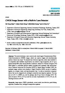
technology. The main objectives of our design are: (1) to evaluate the speed of the sensor, and, in particular, to reach 10 000 frames/s, (2) to demonstrate a versatile and programmable processing unit at pixel level, (3) to provide a original platform dedicated to embedded image processing. The remainder of this paper is organized as follows: first, the section II describes the main characteristics of the overall architecture. The section III is dedicated to the description of the image processing algorithms embedded at pixel level in the sensor. Then, in the section IV, we describe the the details of the pixel design. Finally, we present some simulation results of high speed image acquisition with or without processing at pixel level. 2. OVERALL ARCHITECTURE Figure 1 shows a photograph of the image sensor and the main chip characteristics are listed in Table 1. The chip consists of a 64 x 64 element array of photodiode active pixels and contains 160 000 transistors on a 3.5 x 3.5 mm die. Each pixel is 35 µm on a side with a fill factor of about 25 %. It contains 38 transistors including a photodiode, an Analog Memory, Amplifier and Multiplexer ([AM]²), an Analog Arithmetic Unit (A²U). The chip also contains test structures used for detailed characterization of pixels and processing units (on the bottom left of the chip).
Figure 1 - Photograph of the image sensor in a standard 0.35µm CMOS technology
Technology Array size Chip size Number of transistors Number of transistors / pixel Pixel size Sensor Fill Factor Dynamic power consumption Supply voltage Frame Rate without processing Frame Rate with processing
0.35µm 4-metal CMOS 64 x 64 11 mm2 160 000 38 35 µm x 35 µm 25 % 750 mW 3.3 V 10000 fps 1000 to 5000 fps
x’
y
(1)
y’
(2)
β
x (4)
(3)
Table 1 - Chip Characteristics
3. EMBEDDED ALGORITHMS Our main objective is the implementation of various in-situ image processing using local neighbourhood (spatial gradients, Sobel operator, Laplacian operator, …). So, this compels us to reconsider the processing element structure. Indeed, in a traditional point of view, a CMOS sensor can be seen as an array of independent pixels, each consisting of a photodetector and few transistors mainly dedicated to improve sensor performance as in active pixel sensor or APS (Figure 2.a). PD: Photo Detector PD
PD
PE: Processing Element
PD PD
PE PD
PE PD
PE PD
PE
PD PE
PD
PE
PD
PD PE
PD PE
PD PE
PD PE
PD
PE PD
PD
PE
(a)
The main idea for evaluating these gradients [12] in-situ is based on the definition of the first-order derivative of a 2-D function performed in the vector direction expressed as:
∂V ( x, y ) ∂ξ
(b)
Figure 2 - (a) Photosite with intrapixel processing, (b) photosite with interpixel processing
In our point of view, the electronics, which takes place around the photodetector, has to be a real on-chip analog signal processor which improves the functionality of the sensor. This typically allows local and/or global pixel calculations, implementing some early vision processing. This obliges to allocate the processing resources, so that each computational unit can easily use a neighbourhood of various pixels. In our design, each processing element takes place in the centre of 4 adjacent pixels (Figure 2.b). This distribution is more propitious to the algorithms - embedded in the sensor - which will be described in the following sections.
=
ξ , which can be
∂V ( x, y ) ∂V ( x, y ) cos( β ) + sin( β ) ∂x ' ∂y '
∂V
= (V2 − V4 ) cos(β ) + (V1 − V3 ) sin( β )
(2)
Where Vi (with 1 ≤ i ≤ 4 ) is the luminance at the pixel i i.e. the photodiode output. In this way, the local derivative in the direction of vector ξ is continuously computed as a linear combination of two basis functions, the derivatives in the x and y directions. Using a four-quadrant multiplier, the product of the derivatives by a circular function in cosines can be easily computed. The output P is given by : P= V1 sin(β ) + V2 cos(β ) − V3 sin(β ) − V4 cos( β )
(1)
V1
V2
(2)
Coef1 Coef2
Multipliers
Coef3 Coef4 (3)
V3
V4
(4)
3.1 Spatial gradients The structure of our processing unit is perfectly adapted to the computation of spatial gradients (Figure 3).
(1)
Where β is the vector’s angle. A discretization of the equation (1) at the pixel level, according to the Figure 3, would be given by:
∂ξ
PE PD
Figure 3 –Computation of spatial gradients
Product
Figure 4 - Implementation of four multipliers
(3)
According to the Figure 4, the processing element implemented at the pixel level carries out a linear combination of the four adjacent pixels by the four associated weights (coef1, coef2, coef3 and coef4). To evaluate the equation 3, the following values have to be given to the coefficients: cos( β ) ⎞ ⎛ coef 1 coef 2 ⎞ ⎛ sin( β ) ⎟⎟ ⎜⎜ ⎟⎟ = ⎜⎜ ⎝ coef 3 coef 4 ⎠ ⎝ − sin( β ) − cos( β ) ⎠
(4)
and the horizontal axis (Ih2=I21+I22+I23+I24) can be computed. 3.3 Second-order detector : Laplacian Edge detection based on some second-order derivatives as the Laplacian can also be implemented on our architecture. Unlike spatial gradients previously described, the Laplacian is a scalar (see equation 7) and does not provide any indication about the edge direction.
⎛0 1 0⎞ ∆1 = ⎜ 1 -4 1 ⎟ ⎜ ⎟ ⎝0 1 0⎠
3.2 Sobel operator The structure of our architecture is also adapted to various algorithms based on convolutions using binary masks on a neighbourhood of pixels. As example, we describe here the Sobel operator. With our chip, the evaluation of the Sobel algorithm leads to the result directly centred on the photosensor and directed along the natural axes of the image (Figure 5.a). In order to compute the mathematical operation, a 3x3 neighbourhood (Figure 5.b) is applied on the whole image. j
j+1
(7)
From this 3x3 mask, the following series of operations can be extracted according to the principles used previously for the evaluation of the Sobel operator; ∆1 :
I11=I4-I5 I12=I2-I5 I13=I6-I5 I14=I8-I5
(8)
j+2
4. IMAGE SENSOR DESIGN i
a1
a2 (1)
i+1
a4
i+2
a7
a3 (2)
a5 (4)
4.1 Pixel Design The proposed chip is based on a classical architecture widely used in the literature as shown on the figure 6. The CMOS image sensor consists of an array of pixels that are typically selected a row at a time by a row decoder. The pixels are read out to vertical column buses that connect the selected row of pixels to an output multiplexer. The chip includes three asynchronous output buses, the first one is dedicated to the image processing results whereas the two others provides parallel outputs for full high rate acquisition of raw images.
a6 (3)
a8
a9
(b)
(a)
Figure 5 - (a) Array architecture, (b) 3x3 mask used by the four processing elements
In order to compute the derivatives in the two dimensions, two 3x3 matrices called h1 and h2 are needed:
⎛ -1 0 1 ⎞ ⎛ -1 -2 -1 ⎞ ⎜ ⎟ h 1= -2 0 2 et h 2= ⎜ 0 0 0 ⎟ ⎜ ⎟ ⎜ ⎟ ⎝ -1 0 1 ⎠ ⎝1 2 1⎠
(5)
Within the four processing elements numbered from 1 to 4 (see Figure 5.a), two 2x2 masks are locally applied. According to (5), this allows the evaluation of the following series of operations: h1 : I11=-(I1+I4) I12= I3+I6 I13= I6+I9 I14=-(I4+I7)
h2 : I21=-(I1+I2) I22=-(I2+I3) I23= I8+I9 I24= I7+I8
(6)
with the I1i and I2i provided by the processing element (i). Then, from these trivial operations, the discrete amplitudes of the derivatives along the vertical axis (Ih1=I11+I12+I13+I14)
Figure 6 - Image sensor system architecture
As a classical APS, all reset transistor gates are connected in parallel, so that the whole array is reset when the reset line is
active. In order to supervise the integration period (i.e. the time when incident light on each pixel generates a photocurrent that is integrated and stored as a voltage in the photodiode), the global output called Out_int on the Figure 6 provides the average incidental illumination of the whole matrix of pixels. If the average level of the image is too low, the exposure time may be increased. On the contrary, if the scene is too luminous, the integration period may be reduced.
Operations
Capture sequence Memory 1
Capture sequence Memory 2
Sequential Readout Memory 2
Sequential Readout Memory 1
4.2 Analog Arithmetic Unit (A²U) design
time t0
100 µs
t1
100 µs
which represents the first stage of the capture circuit. The pixel array is held in a reset state until the “reset” signal goes high. Then, the photodiode discharges according to incidental luminous flow. While the “read” signal remains high, the analog switch is open and the capacitor CAM of the analog memory stores the pixel value. The CAM capacitors are able to store, during the frame capture, the pixel values, either from the switch 1 or the switch 2. The following inverter, polarized on VDD/2, serves as an amplifier of the stored value and provides a level of tension proportional to the incidental illumination to the photosite.
t2
Figure 7 – Parallelism between capture sequence and readout sequence
To increase the algorithmic possibilities of the architecture, the acquisition of the light inside the photodiode and the readout of the stored value at pixel level are dissociated and can be independently executed. So, two specific circuits, including an analog memory, an amplifier and a multiplexer are implemented at pixel level. With these circuits called [AM]² (Analogical Memory, Amplifier and Multiplexer), the capture sequence can be made in the first memory in parallel with a readout sequence and/or processing sequence of the previous image stored in the second memory (as shown on Figure 7). With this strategy, the frame rate can be increased without reducing the exposure time. Simulations of the chip show that frame rates up to 10 000 fps can be achieved.
Figure 8 – Frame capture circuit schematic
In each pixel, as seen on Figure 8, the photosensor is a nMOS photodiode associated with a PMOS transistor reset,
The analog arithmetic unit (A²U) represents the central part of the pixel and includes four multipliers (M1, M2, M3 and M4), as illustrated on the Figure 9. The four multipliers are all interconnected with a diode-connected load (i.e. a NMOS transistor with gate connected to drain). The operation result at the “node” point is a linear combination of the four adjacent pixels.
Figure 9 – (a) Architecture of the A²U (b) Four-quadrant multiplier schematic
5. LAYOUT AND PRELIMINARY RESULTS The layout of a 2x2 pixel block is shown in Figure 10. This layout is symmetrically built in order to reduce fixed pattern noise among the four pixels and to ensure uniform spatial sampling. An experimental 64x64 pixel image sensor has been developed in a 0.35µm, 3.3 V, standard CMOS technology with poly-poly capacitors. This prototype has been sent to foundry at the beginning of 2006 and will be available at the end of the first quarter of the year. The Figure 11 represents a simulation of the capture operation. Various levels of illumination are simulated by activating different readout signals (read 1 and read 2). The two outputs (output 1 and output 2) give the levels between OV and VDD, corresponding to incidental illumination on the pixels. The calibration of the structure is ensured by the biasing (Vbias=1,35V). Moreover, in this simulation, the “node” output is the result of the difference operation (out1out2). The factors were fixed at the following values: coef1=-coef2=VDD and coef3= coef4=VDD/2. MOS
transistors operate in sub-threshold region. There is no energy spent for transferring information from one level of processing to another level. According to the simulation’s results, the voltage gain of the amplifier stage of the two [ AM]² is Av=10 and the disparities on the output levels are about 4.3%.
Figure 11– Simulation of (1) high speed sequence capture and (2) basic processing between neighbouring pixels
Figure 10 - Layout of a pixel
6.
CONCLUSION
An experimental pixel sensor implemented in a standard digital CMOS 0.35µm process was described. Each 35 µm x 35 µm pixel contains 38 transistors implementing a circuit with photo-current’s integration, two [AM]² (Analogical Memory, Amplifier and Multiplexer), and a A²U (Analogical Arithmetic Unit). Simulations of the chip show that frame rates up to 10000 fps with no image processing and frame rates from 1000 to 5000 fps with basic image processing can be easily achieved using the parallel A²U implemented at pixel level. The next step in our research will be the characterization of the real chip as soon as possible and the integration on-situ of a fast analog digital converter able to provide digital images with embedded image processing at thousands of frames by second. REFERENCES [1] E. R. Fossum, “Active pixel sensors (APS) : Are CCDs dinosaurs?”, In Proc. SPIE, vol. 1900, pp. 2-14, 1992. [2] E. R. Fossum, “CMOS image sensors: Electronic cameraon-a-chip”, IEEE Transactions on Electron Devices, vol. 44, no. 10, pp. 1689-1698, 1997. [3] D. Litwiller, “CCD vs. CMOS: facts and fiction”, Photonics Spectra, pp. 154.158, 2001. [4] P. Seitz, “Solid-state image sensing”, Handbook of Computer Vision and Applications, vol. 1, 165-222, 2000.
[5] A. El Gamal, D. Yang, and B. Fowler, “Pixel level processing – Why, what and how?”, Proc. SPIE, vol. 3650, pp. 213, 1999. [6] M. J. Loinaz, K. J. Singh, A. J. Blanksby, D. A. Inglis, K. Azadet, and B. D. Ackland, “A 200mW 3.3V CMOS color camera IC producing 352x288 24b Video at 30 frames/s”, IEEE Journal of Solid-State Circuits, vol. 33, pp. 2092-2103, 1998. [7] S. Smith, J. Hurwitz, M. Torrie, D. Baxter, A. Holmes, M. Panaghiston, R. Henderson, A. Murrayn S. Anderson, and P. Denyer, “A single-chip 306x244-pixel CMOS NTSC video camera”, In ISSCC Digest of Technical Papers, San Fransisco, CA, pp. 170-171, 1998. [8] B. M. Coaker, N. S. Xu, R. V. Latham, and F. J. Jones, “High-speed imaging of the pulsed-field flashover of an alumina ceramic in vacuum”, IEEE Trans. of Dielect; Electric. Insul., vol. 2, pp. 210-217, 1995. [9] B. T. Turko, and M. Fardo, “High-speed imaging with a tapped solid state sensor”, IEEE Transactions on Nuclear Science, vol. 37, pp. 320-325, 1990. [10] D. Yang, A. El Gamal, B. Fowler, and H. Tian, “A 640 x 512 CMOS image sensor with ultra wide dynamic range floating point pixel-level ADC”, IEEE Journal of Solid-State Circuits, vol.34, pp. 1821-1834, 1999. [11] S. H. Lim, and A. El Gamal, “Integrating image capture and processing – Beyond single chip digital camera”, In Proc. SPIE, vol. 4306, 2001. [12] Massimo Barbaro et all, “A 100x100 Pixel Silicon Retina for Gradient Extraction With Steering Fiter Capabilities and Temporal Output Coding”, IEEE Journal of solid-state circuits, vol. 37, no. 2, feb. 2002.