Equivalent Circuit Model of Constant On-time Current Mode Control with External Ramp Compensation Shuilin Tian1, Student member, IEEE, Fred C. Lee1, Life Fellow, IEEE, Jian Li2, Member, IEEE, Qiang Li1, Member, IEEE, and Pei-hsin Liu1, Student Member, IEEE 1: Center for Power Electronics Systems Virginia Tech, Blacksburg, VA 24061 USA
[email protected]
2: Linear Technology Milpitas, CA, 95035 USA.
[email protected]
Abstract—Multi-phase constant on-time current mode control based on pulse distribution structure is widely used in Voltage Regulator application for microprocessor. To minimize ripple cancellation effect, external ramp compensation is used in commercial products. However, external ramp will introduce dynamic to the system and AVP requirement will be violated without considering its effect. This paper first studies the effect of external ramp by deriving small-signal transfer function based on describing function method. It is found that external ramp brings additional dynamic, with time constant related with switching period. Then, a simple equivalent circuit model based on three-terminal switch concept is proposed, which considers the effect of external ramp by adding an additional R-L branch. The equivalent circuit model can be reduced to previous unified three-terminal switch model when external ramp is zero and can be reduced to model of constant on-time voltage mode control when external ramp is much larger than inductor current ramp. The proposed three-terminal switch model is a complete model which can be used to examine all transfer functions and is accurate up to half of switching frequency. The model is verified by Simplis simulation. Index Terms---Equivalent circuit model, Constant on-time current mode control, external ramp.
I.
INTRODUCTION
Constant on-time current mode control is widely used to improve light load efficiency in DC-DC converters [1]-[5]. For single phase application, previous research [6]-[8]shows that this structure is inherently stable under all operation range and no external ramp compensation is required as in constant frequency current mode control. For multi-phase application, pulse distribution method is widely used in industry because of its simple implementation and capability of automatic interleaving [3]-[5]. The switch turn off instant is determined by the on time and the switch turn on instant is decided by the comparison of the total inductor current and the control signal from feedback, as shown in Fig. 1. However, when the This work was support by PMC consortium in Center for Power Electronics System, Virginia Tech.
978-1-4799-5776-7/14/$31.00 ©2014 IEEE
operation range is close to ripple cancellation point, the small iL2 iL1 iLsum vc
Se Tsw/2
d1 Ton d2
Ton 180̊
Ton
Ton
(a) (b) Fig. 1. (a) block diagram (b)steady-state waveform of two-phase constant on-time current mode control with external ramp based on pulse distribution
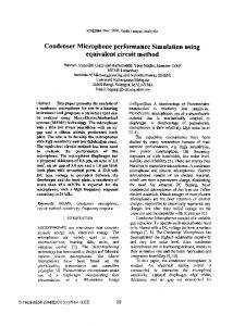
(a) (b) Fig. 2. Jittering performance comparison for a three-phase converter (a) D ≈ 0.25 (b) D ≈ 0.3, very close to cancellation point (0.33)
amount of total inductor current ripple is prone to be disturbed by noise. Fig. 2 shows the experimental results of jittering performance for a three-phase Buck converter, when duty cycle is around 0.3, which is very close to ripple cancellation point (D=33%), Severe jittering is observed. As shown in Fig. 1, external ramp compensation is utilized as a simple solution to alleviate jittering problem in commercial products [3][4][5]. The external ramp increases the total ramp to compare with control signal and therefore the immunity of the circuit to the disturbing noise is improved. The addition of external ramp improves the jittering performance, but it also affects the dynamic performance. Without changing the compensator parameters, it is observed that the introduction of the external ramp reduces the bandwidth and phase margin of the total loop gain transfer function. One example is shown as Fig. 3 with the following parameters: nph=2; Fsw=800kHz/phase, Vin=5.2V, Vo=2V, Ls=150nH/phase, RLL=1.5mΩ, Io=40A. Without external
3747
ramp, the converter is designed with sufficient phase margin (70degrees). With the external ramp slope around the inductor current falling slope (magnitude of 38mV), the phase margin reduce to 50degrees while the bandwidth reduce from 200kHz to 150kHz. With external ramp slope around 2 times the inductor current falling slope, the phase margin further reduces to 38degrees, which is out of many engineer’s comfort zone of at least 45 degree phase margin.
T2 ( s )
Fsw_eq/2
40
Gain (dB)
20 0
Se=0 Se=1sfs=38mV Se=2sfs=76mV
− 20
Phase (Deg)
− 40 0
− 30 − 60
70̊
− 90 − 120
38̊
− 150 − 180 1×10³
4
1×10
50̊
1×10⁵
Frequency (Hz)
Se=0 Se=38mV Se=76mV 1×10⁶
phase constant on-time current mode control with external ramp compensation, the accurate small-signal control-tooutput voltage transfer function is derived using describing function method as in [7] and the results are presented in section II. The describing function result is infinite order and accurate up to infinite frequency. In section III, the infinite order transfer function is simplified to polynomial form in order to derive a simple equivalent circuit model. It is found that external ramp introduces a static zero and a moving pole which is related to the slope of external ramp. Physically it reveals the fact that external ramp turns the circuit into a nonideal current source. Based on the non-ideal current source, a three-terminal switch model is proposed, an additional impedance branch comprised by a resistor and an inductor is utilized to represent the non-idealness of the current source. The proposed equivalent circuit model is an extension of previous three terminal switch model for current mode control [8]. It is a complete model which can be used to examine all transfer functions and is accurate up to half of switching frequency. Section IV discusses some important aspects about the proposed three-terminal switch model. Section V extends the three-terminal switch model to multiphase converters. Section VI provides simplis simulation results to verify the proposed three-terminal switch model. Section VII summarizes this paper.
Fig. 3. Impact of external ramp on loop gain bandwidth and phase margin in 2-phase VR example.
For quantitative analysis, an accurate small-signal model is indispensable. Several papers which are closely related to this subject are published and summarized as follows: In [7], the describing function method is used to derive the smallsignal control to output voltage and audio susceptibility transfer function for current mode control, but the results there does not cover constant on-time current mode control with external ramp case. In [8], a unified three-terminal switch model for current mode control is proposed taking input property into consideration. The equivalent circuit model does not include constant on-time current mode control with external ramp case either. In [9], the describing function method is used to derive the transfer function of variable frequency modulator. However, the inductor current information is not included in voltage mode control structure. In [10]-[13], small signal analysis for constant on-time V2 control (or ripple based control) and constant frequency V2 control with external ramp compensation are presented. However, in V2 control or ripple based control structure, not only inductor current ramp participates in modulation, but also capacitor voltage ripple. In short, up to now, no good small signal model for constant on-time current mode control with external ramp compensation is proposed in the literature.
II. SMALL-SIGNAL TRANSFER FUNCTION BASED ON DESCRIBING FUNCTION METHOD To get exact small-signal control-to-inductor current transfer function, the describing method which is first proposed in [7] for current mode control is employed. The structure of constant on-time current mode control with external ramp compensation when vc is under perturbation is shown in Fig. 4, the nonlinear constant on-time modulator, which consists of the switches, the inductor current, the comparator with external ramp and the on-time generator, is treated as a single entity. The steady-state waveform and perturbed waveform is shown in Fig. 5. The methodology of the describing method, assumptions and derivation steps are exactly same as [7], therefore, only critical steps are listed in this paper.
This paper tries to provide a simple and accurate three terminal switch model for constant on-time current mode control with external ramp compensation, which will serve as a useful tool for understanding the effect of external ramp and designing feedback control appropriately. The remaining paper is organized as follows: firstly, starting from a single
3748
iL Ls Vin
+-
RCo + Co
Driver
RL
d
Ton
+ +
vc ~
vc=Vc+ vc
Fig. 4. Modelling method for constant on-time with external ramp. Sf
Sn Se
Vc
vc(t)
PWM
Toff
Ton
PWM’
Toff(1)
Ton Toff(2) t2
t1=0
t3
t4
t5
t6
Fig. 5. Steady-state and perturbed waveform for constant on-time current mode control with external ramp compensation.
Fsw/2 60
vc (t i −1 + Toff ( i −1) ) + s e Toff (i −1) + s nTon = vc (t i + Toff (i ) ) + ( s e + s f )Toff (i )
Gain (dB)
Step 1: perturbed off-time calculation (1)
Step 2: perturbed duty cycle and perturbed inductor current calculation
i L (t )
M
0 ≤ t ≤ t M +Toff
( M ) +Ton
0 ≤ t ≤ t M + Toff ( M ) + Ton
= ∑ [u (t − t i − Toff ( i ) ) − u (t − t i − Toff (i ) − Ton ) i =1
⎧ ⎫⎪ − Vo V t⎪ V = ∫0⎨ in d (t ) − o [1 − d (t )]⎬ ⋅ dt + i L 0 L L ⎪⎩ ⎪⎭ s s
(2)
f s (1 − e V in ) iL (s) = v c ( s ) ( s e + s f ) − s e e − sT sw L s s
(4)
vo (s) f s (1 − e − sT on ) V in R L ( R Co C o s + 1) = vc (s) ( s e + s f ) − s e e − sT sw L s s RLCo s + 1
(5)
Step 4: Consider the variation of inductor current slopes, the transfer functions from the input voltage to inductor current and output voltage to inductor current are derived similarly and the results are shown as follows: i L (s) f s (1 − e − sTon ) −1 (1 − e sTon ) = ⋅ Vin + D] [ − sTsw sTsw (6) vin (s) Ls s (1 − e )[(s f + s e ) − se e ] s ⋅ Ls / Ri
Se=Sf
45
Se=0 Se=Sf
0
1×10
3
1×10
4
1×10
5
1×10
Frequency (Hz)
6
Fig. 6. Comparison of control to inductor current transfer function between first order approximation (8) and simplis simulation.
From Fig. 6, if there is no external ramp, the control to inductor current is constant gain, which reveals the fact that in this case the inductor current is well controlled by control signal, or equivalently, the circuit can be regarded as an ideal current source. By adding an external ramp, the gain of control to inductor current drops at high frequency, which reveals the fact that the external ramp reduces the ability of controlling the inductor current, or in other words, the circuit is a non-ideal current source due to the effect of external ramp. Based on the physical insight of non-ideal current source, an equivalent circuit is derived to represent (8) as follows: Ls v^c/Ri
Re2
(7)
Le2
^iL
v^o RCo RL
+ Co
Fig. 7. Equivalent circuit representation of constant on time current mode control with external ramp compensation for small duty cycle.
III. THREE-TERMINAL SWITCH MODEL FOR SINGLE PHASE CONVERTER
The expressions of Re2 and Le2 is shown as follows:
For small duty cycle application, the effect of dynamic term related with on time in (4) is small and can be neglected. Furthermore, with a first-order polynomial simplification, the infinite order control-to-inductor transfer function shown in (4) is simplified as follows: Tsw s V 2 , s f = Ri ⋅ o Ls ⎛s ⎞ 1 1 + ⎜ e + ⎟Tsw s ⎜ sf 2 ⎟ ⎝ ⎠
30
− 90 100
− sT on
iL ( s) 1 ≈ v c ( s ) Ri
Se=0
− 45
(3)
Step 3: Fourier analysis on inductor current and output voltage to obtain describing function result:
i L ( s) f s (1 − e − sTon ) 1 1 = ⋅[ ⋅ ⋅ Vin − 1] vo (s) Ls s (se + s f ) − se e −sTsw s ⋅ Ls / Ri
40
20 90
Phase (Deg)
d (t )
50
1+
(8)
The approximation is good up to half of switching frequency compared with simulation results, as shown in Fig. 6.
Re 2 =
Ls L , Le 2 = s se s Tsw 2 e sf sf
(9)
For general case, the effect of dynamic term related with on-time in (4) may need to be considered: as the duty cycle is large, additional phase delay is observed. Previous equivalent circuit model of constant on time control uses an impedance comprised by Re and Ce to represent the additional phase delay by forming a pair of double pole whose position is related with on-time [7]. Apply the same concept, the polynomial simplification of control-to-inductor current and its equivalent circuit representation is shown as (10) and Fig. 8, respectively.
3749
iL (s) 1 ≈ v c ( s ) Ri
Q1 =
2
π
IV. DISCUSSION ON PROPOSED THREE-TERMINAL
Tsw s 1 2 2 ⎛s ⎞ ⎛ s ⎞ 1⎟ s e ⎜ ⎟ ⎜ 1+ + T s 1+ + ⎜ s f 2 ⎟ sw Q1ω1 ⎜⎝ ω1 ⎟⎠ ⎝ ⎠
,ω1 =
1+
SWITCH MODEL
A. Comparison with previous three-terminal switch model[8]
(10)
As seen from (9), the impedance comprises by Re2 and Le2 is infinite when there is no external ramp, therefore, additional Re2-Le2 branch disappears and the model in Fig. 9 reduces to previous model proposed in [8], which means the model shown in Fig. 9 is more inclusive and general.
π Ton Ls
^vc/Ri
Re2
Re
^
^vo
iL
B. The effect of Re2-Le2 Impedance RCo
Ce
RL
+
Le2
Co
Fig. 8. Equivalent circuit representation of constant on time current mode control with external ramp compensation for general case.
2 Ls
1 , Ce = Lsω12 ⎛ 2s ⎞ ⎜ e + 1⎟T ⎜ sf ⎟ on ⎝ ⎠ Ls Ls Re 2 = , Le 2 = se se (1 − D)Tsw 2 (1 − D) sf sf
Re =
(11)
Fig. 8 can be used to derive control-to-output voltage transfer function and output impedance, however, the input property is lost. To consider the input property and apply the three-terminal switch model concept, the same strategy as [8] is adopted. The three-terminal switch model for single phase is shown as Fig. 9.
a +-
c
iL
vo
Ls
Vin
RCo + Co
Ri
Driver
p
d
RL
When external ramp increases, the impedance Re2 and Le2 reduces. To illustrate this point, use Se=Sf as an example. The values of Re2 and Le2 can be calculated from (9), which is Ls/(Tsw) and Ls/2, respectively. When modulation frequency is low, the impedance of Re2 is much larger than Le2 and Ls, therefore, the Re2-Le2 impedance does not shunt current, all the current from the current source flows into Ls branch, therefore, the gain is flat, as seen from Fig. 6. When modulation frequency increases, the impedance of inductor Ls branch increases, and the Re2-Le2 branch starts to shunt current. According to current divider theory, the boundary modulation frequency is the point at which the impedance of Re2 is the same as the sum impedance of Le2 and Ls. For this example, the values is fsw/(3π). After modulation frequency surpasses this frequency, Re2-Le2 branch starts to shunt current as the impedance is smaller compares with Ls branch. The inductor current is determined by an ideal current source coming through a first order current divider. The larger the modulation frequency, the smaller the Re2-Le2 impedance compared with Ls branch, the more current it shunts and the more phase delay. From Fig. 6, the gain and phase both continue to drop which is a pole effect. Now if the modulation frequency further increases to surpass the critical point where the impedance of Re2 is the same as impedance of Le2, then impedance of Le2 will dominate Re2-Le2 branch and the ratio between this branch and Ls branch is same afterwards. Therefore the gain starts to drop and the phase increases, which is a zero effect. The frequency of zero is at fsw/π. In general, due to the branch of Re2-Le2, there is a moving pole and a static zero, the pole is determined by Re2, Le2 and Ls, the zero is determined by Re2 and Le2. The expression of the zero and the pole is shown as follows:
-
Ton
+ +
Hv
vc
vref
f pe =
(a) v^ap*Kap ^ vc*Re/DRi
a
-
DIc
I vˆL ⋅ ( c ) Vap I vˆcp ⋅( c ) Vap
+
-
+
−
Vap
Ls Re
D⋅iˆRe2
1
D ^ iRe2
Re2 Le2
1 Re 2 Fsw f ze = = 2π Le 2 π
c
+ v^L Ce
p
(b) Fig. 9. Three-terminal switch model of single phase constant on time current mode control with external ramp compensation.
Re 2 Fsw 1 = , 2π Le 2 + Ls π ( 2 se / s f + 1)
(12)
C. The effect of external ramp
Previously the effect of Re2-Le2 impedance with a given external ramp is discussed: a pole and zero is introduced by the additional Re2-Le2 branch. From (12), the zero position is stationary while the pole position is dependent with the magnitude of external ramp. To understand why the pole position is dependent with the external ramp physically, the
3750
natural response of the circuit in time-domain is examined, as shown in Fig. 10. The solid line is steady state of the sensed inductor current waveform while the dashed line is the purebred waveform. At time t0, there is a perturbation on the inductor current ΔiL0, after k switching cycles, the perturbation value changes to ΔiLk. The relations between ΔiLk and ΔiL0 can be derived as follows:
combines with the low frequency pole and forms a double pole at power stage corner frequency, in this case, the current loop effect is killed by the large external ramp, changing current mode to voltage mode control.
0.64
(13)
j ω sw
2
1
k
⎛ s ⎞ e ⎟ Δi Δi Lk = ⎜ ⎜ se + s f ⎟ L 0 ⎝ ⎠
Im
Increasing Se
2
0 .5
1
0.25
0.7 5
LC
Re iL * Ri Δ iL 0 R
Vc
0.7 5
sn
sf
i
Δ iL1 R i
0.64
…
0 .5
0.25
9.4 2e+00 5
Δ i Lk R i
1
Se
t0 Fig.10. Natural response of constant on-time current mode control with external ramp compensation.
jω
sw 2
Fig. 11. Pole-zero map with increasing external ramp.
From (13), without se, the perturbation is disappeared in just one cycle, with external ramp, the dynamics is observed, the larger external ramp, the more time it requires to damp out the perturbation, as the coefficient in (13) is closer to 1. From (13) a first order dynamic response is observed and the time constant is related with external ramp. Physically, without external ramp, the inductor current does not contribute to any dynamic for constant on-time structure, with addition of external ramp, the inductor current information is read and it participates in the dynamic again. That explains the dependence of the pole on the external ramp magnitude.
Gain (dB)
vo ( s ) vc ( s )
Phase (Degree)
Fig.11 shows the pole zero map with different external ramp and the following circuit parameters: Fsw=300kHz, Vin=12V, Vo=1.2V, Ls=300nH, RL=100mΩ, 8 ceramic capacitors (1.4mΩ/100uF), Ri=10 mΩ. The ESR zero of the capacitor is far away from the switching frequency and can be ignored. From Fig. 7, when external ramp is zero, Re2-Le2 impedance is infinite and only the pole caused by output capacitor and load exists. When external ramp increases, Re2Le2 branch impedance decreases and starts to shunt current in a certain frequency range. As analyzed in previous section, there is a stationery zero located at fsw/ π, which is determined by Re2 and Le2 and a moving pole which is determined by Re2, Le2 and Ls, as shown in (12). Further increase the external ramp, the impedance of Re2-Le2 branch is so small that the current loop effects is killed by the large external ramp, turning the current mode control into voltage mode control. The moving pole combines with the single pole caused by output capacitor and load and forms a pair of double pole at power stage LC filter corner frequency.
−
2
Fsw/2
40
Se=0Sf Re2=∞ Se=1Sf Re2=0.1Ω Se=4Sf Se=20Sf
20 0 − 20 − 40 − 60
0 − 30 − 60 − 90 − 120 − 150 − 180 100
3
1×10
1×10
4
1×10
5
1×10
6
Frequency (Hz) Fig. 12. Bode plots of control-to-output voltage transfer function with increasing external ramp.
D. Comparison with constant on-time voltage model [9]
Compare the pink curve in Fig. 12 with control-to-output voltage transfer function of constant frequency voltage mode control, it is found the gain curve is very similar while the phase curve is quite different as phase boost is observed at high frequency due to the effect of stationery zero. The phase boost is first pointed out in [9], where the describing function method is utilized to derive the transfer function of variable frequency modulation scheme. The control-to-output voltage transfer function is shown in the following equation [9]:
Fig. 12 shows the bode plots of control to output voltage transfer function with increasing external ramp. When se=0 (red), only one pole caused by output capacitor and load exists and it is first order circuit as the minimum phase is around -90 deg. When Se=1sf (blue), the pole starts to move and split with the zero. When Se=20sf (pink), the moving pole
3751
DVin se Tsw
Gc 2 vo _ v =
ωo =
1 LC
1 + RCo C o s ⎛ s 1 + s /(Qo ω o ) + ⎜ ⎜ω ⎝ o
, Qo ≈ R L
⎞ ⎟ ⎟ ⎠
2
e
1− D Tsw s 2
Following the same reason, for n-phase converter under duty cycle no-overlap case, the rising slope and falling slope for summed inductor current is shown as follows:
, (14)
sn _ n =
C L
(16)
Fig. 13 shows comparison of control to output voltage transfer function between constant on-time voltage mode shown in (14) and constant on-time current mode model shown in Fig. 8 under Se=1000sf case. The extreme external ramp almost kill effect of the current loop and turns the circuit into a voltage mode control, as shown in Fig.13, the two models agree very well. There is a slight difference in high frequency phase due to the first order polynomial approximation when deriving constant on-time current mode control while the model shown in (14) use exponential term to represent the phase boosting phenomenon.
Gain (dB)
vo (s) vc (s)
Se=1000Sf
iL
Fs/2
vo
Ls/n
+ vin/n -
Driver
− 10
RCo RL + Co
Ri
Ton
− 40
vc
+
Tsw/n
− 70
90
Se
Fig. 14. Equivalent single phase constant on-time current mode control
Constant on voltage mode
Therefore, the equivalent circuit model for multi-phase constant on-time current mode control with external ramp compensation can be derived, as shown in Fig. 15.
Constant on current mode 0
v^ap*Kap_n ^ vc*Re_n/nDRi
a
1×10
3
4
1×10
5
1×10
Frequency (Hz)
1×10
−
6
To extend the proposed three-terminal switch model to multi-phase constant on-time current mode control case, the summed inductor current signal should be examined carefully as it is the feedback signal to determine the duty cycle. The strategy is to derive an equivalent single-phase converter and then use the equivalent circuit model of single-phase converter. For a two-phase converter shown in Fig. 1, the rising and falling slope of summed inductor current is shown as follows: 2V V Vin − 2Vo Vin / 2 − Vo ,sf _2 = o = o = Ls Ls / 2 Ls Ls / 2
I vˆL ⋅( c ) Vap
Re_n
nD⋅iˆRe2_n
1
Re2_n
nD Le2_n ^ iRe2_n
+ ^ v L
Ce_n
p
Fig. 13. Control-to-output voltage comparison between constant on-time voltage mode and constant on-time current mode under se=1000sf.
V. EXTENSION TO MULTI-PHASE CONSTANT ON-TIME CURRENT MODE CONTROL
nDIc
I vˆcp ⋅( c ) Vap
-
-
− 180 100
Vap
Ls/n
+
− 90
+
Phase (Deg)
From (16), for n-phase constant on-time current mode control structure, from small-signal point of view, it is equivalent to the single-phase constant on-time control, as shown in Fig. 14. The equivalent switching frequency is n times that of single phase, the inductor is reduced to 1/n of the single phase inductor and the input voltage is also reduced to 1/n.
20
− 100
sn _ 2 =
nV o Vo Vin − nV o V in / n − V o ,sf _n = = = Ls Ls / n Ls Ls / n
Fig. 15. Complete three-terminal switch model of n-phase constant ontime current mode control with external ramp compensation.
The expressions of Re_n, Ce_n, Re2_n and Le2_n are shown in (17) and the expressions of pole and zero caused by external ramp are shown in (18):
(15)
3752
2 Ls / n n , Ce = Lsω12 ⎛ 2s ⎞ ⎜ e + 1⎟T ⎜ s f _ n ⎟ on ⎝ ⎠ Ls Ls / n , Le 2 = Re 2 = se s (1 − nD)Tsw 2 e (1 − nD) sf _n sf _n Re =
(17)
c
f pe _ n =
se =1sf vo ( s) vc ( s )
(18)
1 Re 2 _ n Fsw / n = π 2π Le 2 _ n
Gain (dB)
f ze =
Re 2 _ n Fsw / n 1 , = 2π Le 2 _ n + Ls / n π ( 2 s e / s f _ n + 1)
Gain (dB)
40
Fs/2
20 0 − 20
Z in ( s )
− 40 − 60 100
1×10
3
4
1×10
90
1×10
5
Fs/2
1×10
6
Gain (dB)
Gain (dB)
vo ( s ) vc (s )
0
− 40 − 60
3
1×10
1×10
4
80
1×10
5
1×10
3
1×10
1×10
4
5
1×10
Frequency (Hz) Equivalent Circuit Model Simplis Simulation
6
1×10
− 20
− 20
Phase(deg)
− 40
− 40 1×10
3
4
1×10
1×10
5
1×10
Fs/2
6
− 60 100
1×10
3
4
1×10
1×10
5
1×10
6
Fs/2
90
0
− 90
-60deg 1×10
3
1×10
4
5
6
1×10
1×10
− 60 100
1×10
3
4
1×10
1×10
5
Fs/2
90
1×10
− 90
− 90
-80deg
− 180 100
3
1×10
1×10
4
1×10
5
1×10
Frequency (Hz)
6
-100deg
− 180 100
1×10
3
1×10
4
5
1×10
1×10
Frequency (Hz)
Switching Circuit Simplis Simulation
Fig. 17. Simplis verification of control to output voltage transfer function for single phase constant on-time current mode control with various duty cycles and se=1sf.
Fig.18 shows verification of control to output voltage transfer function with different external ramps and 0.1 duty cycle, in all cases, the model agrees well with simulation result up to ½ fsw. When external ramp is large, the circuit changes from first order current mode control to second order voltage mode control, with high frequency phase boost due to the stationery zero. Fsw/2
vo ( s ) 40 vc ( s )
6
20
20 0
1×10
3
4
1×10
0
1×10
5
1×10
6
− 20
− 90 60
− 40 − 60 − 80 − 100 100
0
1×10
3
1×10
4
5
1×10
Frequency (Hz)
1×10
Se=0Sf
− 20
Se=1Sf Se=4Sf Se=40Sf
− 40
Fs/2
6
Equivalent Circuit Model Simplis Simulation
0
− 90
Fig. 16. Simplis verification for single-phase constant on-time current mode control with D=0.1 and Se=1Sf.
− 180 100
Fig. 17 shows verification of control-to-output transfer functions for different duty cycles with se=1sf. For all cases, the proposed equivalent circuit model shown in Fig. 9 agrees very well with simulation results up to 1/2 fsw. When duty cycle is larger, the phase boost is less: as shown in Fig. 17, at 1/3 fsw, for D=0.1, the phase is -60deg, while for D=0.5 and D=0.9, the phases drop to -80 and -100, respectively. The phenomenon is consistent with the conclusion from [9], where it is found that the phase leading property of the constant on-time modulator is related with off-time: Larger duty cycle means smaller off-time, which leads to smaller phase leading.
3
1×10
1×10
4
5
1×10
Frequency (Hz)
1×10
6
Fig. 18. Simplis verification of control-to-output voltage transfer function for single-phase constant on time current mode control with different external ramps.
Fig. 19 shows simulation verification of two-phase constant on-time current mode control with the following parameters for each phase: Fsw=800kHz, D=0.4, Vin=5.2V, Vo=2V, Ls=150nH, Ri=10mΩ, Total output capacitors are 20 ceramic capacitors (22uF/5mΩ). The control to output voltage and audio susceptibility transfer functions predicted by equivalent circuit model shown in Fig. 15 agree very well with simplis simulation results up to ½ fsw.
3753
6
0
0
Phase(deg)
− 180 100
Gain (dB)
Phase(deg)
Z o (s)
0
− 20
40
− 40 100
− 90
40 20
Equivalent Circuit Model
− 20
0
0
Frequency (Hz)
Fs/2
60
20
0
90
− 80 − 100 100
20
− 180 100
Fs/2
− 20
40
Gain (dB)
vo ( s) v in ( s )
D=0.1,se =1sf
Fs/2
Fs/2
40
− 60 100
VI. SIMULATION VERIFICATION Fig. 16 shows simulation verification for single phase constant on time current mode control with the following parameters: Fsw=300kHz, Vin=12V, Vo=1.2V, Ls=300nH, RL=100mΩ, 8 OSCON capacitors (6mΩ/560uF), Ri=10mΩ, se=1sf. All four transfer functions including control-to-output voltage, audio susceptibility, output impedance and input impedance are compared. The results from proposed equivalent circuit model shown in Fig. 9 agrees with simulation results well up to 1/2 fsw for all transfer functions.
Fs/2
− 40
Compare (17), (18) with single phase equations (11) and (12), the pole and zero position are higher as the equivalent switching frequency is n times the switching frequency of single phase.
D=0.9
D=0.5
D=0.1
6
v o ( s ) 20 v in ( s ) 0
Gain (dB)
Se=0Sf
− 10
[10] Se=0
− 40
Se=2Sfs
− 25
− 60
Equivalent Circuit Model
90 − 40
− 80 90
Phase(deg)
Simplis Simulation 0
− 90
− 180 100
1×10³
1×10⁴
1×10⁵
1×10⁶
Equivalent Circuit Model
[11]
3
Simplis Simulation 0
[12] − 90
− 180 100
Frequency (Hz)
[13] 1×10³
1×10⁴
Frequency (Hz)
1×10⁵
Fig. 19. Simplis verification of control to output voltage transfer function and audio susceptibility for 2-phase constant on time current mode.
VII. SUMMARY AND CONCLUSION This paper analyzes the effect of external ramp on smallsignal model of constant on-time current mode control. It is found that external ramp brings additional dynamics by introducing a moving pole and a static zero. A three-terminal switch model is proposed based on non-ideal current source concept, where the non-idealness of the current source is presented by a Re2-Le2 branch. The equivalent circuit model is a complete model and can be used to examine all the transfer functions. The equivalent circuit model is an extension of previous unified three-terminal switch model proposed in [8] and can be reduced to constant on time voltage mode model [9] when external ramp is extremely large in which case the effect of current loop is negligible. The model is extended to multi-phase current mode control and is verified with simplis simulation results. REFERENCES [1]
[2] [3] [4] [5]
[6]
[7]
[8]
[9]
Se=2Sfs
− 20
Gain (dB)
5
Phase(deg)
Fsw
Fsw_eq/2
v o ( s ) 20 vc ( s )
Analog Devices, ADP2102 datasheet, http://www.analog.com/static/importedfiles/data_sheets/ADP2102.pdf. Linear Technology, LTC3709 datasheet, www.linear.com/docs/6026 Texas Instruments, TPS59650 datasheet, http://www.ti.com/product/tps59650. Dec, 2011. Richtek Cooperation, RT8859M datasheet, http://www.richtek.com/product_detail.jsp?s=873. Sep, 2013. US Patent: 8,159,197 B2, C. Cheng, J. Huang, and C. Li, “CIRCUIT AND METHOD FOR CONSTANT ON-TIME CONTROL FOR AN INTERLEAVED MULTIPHASE VOLTAGE REGULATOR,” Apr., 2012. R. B. Ridley, “A new continuous-time model for current-mode control with constant frequency, constant on-time, and constant offtime, in CCM and DCM,” in proc. IEEE PESC’90, pp. 382- 389. J. Li and F. C. Lee, “New modeling approach and equivalent circuit representation for current-mode control,” IEEE Trans. Power Electron., vol. 25, no. 5, pp. 1218–1230, May 2010. Y. Yan, F. C. Lee, and P.Mattavelli, “Unified three-terminal switch model for current mode controls,” IEEE Trans. Power Electron., vol. 27, no. 9, pp. 4060–4070, Sep. 2012.
3754
J. Sun, “Small-signal modeling of variable-frequency pulse width modulators,” IEEE Trans. Aerosp. Electron. Syst., vol. 38, no. 3, pp. 1104–1108, Jul. 2002. S. Tian, F. C. Lee, P. Mattavelli, K. Y. Cheng, and Y. Yan, “Smallsignal Analysis and Optimal Design of External Ramp for Constant On-Time V2 Control with Multilayer Ceramic Caps,” IEEE Trans. . Power Electron., vol.29, no.8, pp.4450-4460, Aug. 2014. S. Tian, K. Y. Cheng, F. C. Lee and P. Mattavelli, “Small-signal model analysis and design of constant on-time V2 control for lowESR caps with external ramp compensation,” in Proc. IEEE ECCE, 2011, pp. 2944-2951. S. Tian, F. C. Lee, P. Mattavelli, Y. Yan, “Small-signal analysis and design of constant frequency V2 peak control,” in Proc. IEEE APEC, 2013.pp. 1717 - 1724. S. Tian, F. C. Lee, P. Mattavelli and Y. Yan, “Small-signal Analysis and Optimal Design of Constant Frequency V2 Control,” IEEE Trans. Power Electron., accepted and to be published.