-
The 30th Annual Conference ofthe IEEE Industrial Electronics Society, November 2 6,2004, Busan, Korea
Investigation of Voltage Dip Restorer Using Square Wave Inverter K.W.E.Cheng, Y.L.Ho, S.L.Ho, K.P.Wong, NCCheung and T.K.Cheung Department of Electrical Engineering, The Hong Kong Polytechnic University, Hong Kong. e-maiI :
[email protected]
Abstrm-The concept of square wave compensation is studied for the application to the voltage dip restorer in this paper. Both single square wave and dual square wave are used in this analysis. Both methods have shown to have a fast dynamic response as compared to sinusoidal compensation. The dual square wave can also compensate far the zerocrossing and the distortion is small. Experimental results confirm the proposed method.
high intensity application. They will also be extinguished and cannot be tumed on for 5-10 minutes because of the natural property of the lamp. Another problem is the transient problem that occurs due to rapid switching or surge that occurs for a much shorter duration and may be less than a cycle of the mains frequency. The common reasons can be summarized as:
1. INTRODUCTION
a. b. c.
The use of electronics in everyday activities creates problems of power quality. Voltage dips in distribution networks caused by system faults can adversely affect many highly sensitive end-user devices. The power supplies in many cases are then interrupted. The implied financial losses may be very high and could also be dangerous when systems are used for life-saving. Voltage dip are mainly caused by system fault of improper design when a high current 111. which in turn lead to a voltage drop across the network impedance. The voltage dip may be caused by [ 5 ] : a.
b. c. d. e.
Distribution or transmission network fault Switching of large load such as HVAC and large heating elements Cable fault due to construction Lightning strike that trips a breaker In high rise building, the distribution networks are clustered together and are electrically coupled to others especially no separate trunkings are used. Any major fault in a building may cause voltage dip to an adjacent network or building.
Voltage dip disturbs many types of devices connected to the network and is one of the most frequent causes of power quality problems. A voltage dip of hundred milliseconds may have damaging consequences for a prolonged period. The major damages are: a.
b. c. d.
Motors may not be maintained at required speed even for a good variable speed drives. Motor contactors drop out with around 65% of the nominal voltage Many variable-speed drives trip out when a voltage dip is more than 15%. Voltage sag (dip) causes premature aging of electronic equipment and lighting elements. Some lighting unit is extinguished when voltage drop is below 20%. Today, the HID lamps are being use for
d. e. f.
Atmospheric phenomena Switching ordoff large loads Tum-on and off of rapid switching of power lines and capacitor banks Fault current High frequency switching electronics such as inverter for motor dnves and UPS. Earthing problem or lightning causes a flash over due to excessive charge established and high potential difference.
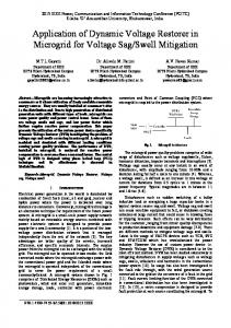
Recently, dynamic voltage restorer (DVR) [3-61 has been used for the protection and installed in distribution network. When a fault occurs in a distribution network, a sudden voltage dip will appear on adjacent load feeders. With a DVR installed on the associated path, the line voltage i s restored within very short period and hence the equipment, apparatus and sensitive device will not be affected. A DVR usually consists o f an isolation transformer, harmonic filter, voltage source converters, energy storage component, control electronics and solid state switch. One of the existing problems of the DVR is that dynamic performance of the device. It is necessary for the device to response to the voltage dip within a few milliseconds. The energy storage components must also be optimized in terms of the size, duration of the voltage dip and amount of voltage dip. The harmonic generated by the switching converter must be properly filtered. The reliability of the DVR is another concern. The present technology cannot solve all the above shortcomings, and the optimization design has not been analyzed thoroughly.
The power density of a DVR is also a challenge [7]. The current design method requires a bulky transformer for the isolation and voltage matching. The power density of DVRs is therefore poor and the material cost is therefore high. It is possible to use high frequency transformer for the replacement.
0-7803-873C-9/04/$20.00 02004 IEEE
204 Authorized licensed use limited to: Hong Kong Polytechnic University. Downloaded on July 14, 2009 at 03:40 from IEEE Xplore. Restrictions apply.
Other than the basic DVR, the recent development in power conversion also provides other methods of solution to the above problems. This includes new topologies proposed for power conversion and isolation that give altemative methods for the switching electronics [S-111. High frequency transformer and inductor design techniques give advanced method to design high frequency magnetic energy storage and isolation E12-141. Switched-capacitor techniques [ll-151 give the latest method for switching capacitor operation and energy storage. Power factor correction (PFC) with resonant switching gives low EM1 for the improvement of power quality [ 161.
is especially important for high power application which the size is a paramount factor for the system cost and size.
11. CLASSICAL COMPENSATIONMETHOD
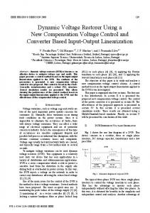
The classical method is to use an inverter to produce the sinusoidal voltage and its amplitude is varied according to the required output voltage of the system after a voltage dip. The usual method is to regulate the inverter's output in order to maintain constant output voltage in the critical devices. Fig 1 shows a schematic diagram of the situation. ZL and CB are line impedance and circuit breaker respectively. The energy storage, inverter, transformer and filter form the large components of a DVR. A Static Triac is usually used to bypass the DVR when there is no fault. It can be seen that when there is a fault appeared in Load 1, the inverter is triggered to generate a sinusoidal voltage that is added in series to the bus of the load 2. Usually, a transformer is used for isolated and to connect the inverter output voltage in series with the bus [ 171. However, a filter is needed to remove the pulse width modulated high frequency carrier. The drawback is that the voltage requires considerable time to rise to required voltage because of the delay due to the filter [17]. Fig 2 shows that the output voltage from the inverter and the voltage takes a few cycles to reach the required value.
Tine (ms)
Fig 2: The voltages of the source, inverter and load under a voltage sag with the compensation of a DVR using sinusoidal modulation.
111. H G 3 FREQUENCY W S F O M E R TECHNLOLOGY
A. High frequency transformer With the rapid development of high frequency power electronics, the isolation can be undertaken by a high frequency power converter. A schematic is shown in Fig 3. It can be seen that using a high frequency transformer in the D O C converter side, the 50Hz low frequency transformer can be eliminated and the same isolation can therefore be provided. It should be noted that the size of the filter component for the inverter cannot be reduced as it is for filtering the switching component and to pass the 50Hz power. The high Frequency transformer is actually operated at the switching frequency of the D O C converter. The converter has input and output voltages both in DC and its isolation and voltage stepping are provided by the high frequency AC transformer. m
w**.
r
,-.r
I
Fig 3: High frequency transformer used i n a DVR
Fig I : Schematic of a classical DVR
B. DC/DC converter Another drawback of the proposed method is that the transformer has to handle through 50Hz main frequency power. As the magnetic field is inversely proportional to the operational frequency, therefore it is necessary to increase the transformer size in order to reduce the magnetizing magnetic field of the transformer core. As a result, the size of the transformer is increased and it will significantly increase the size and cost of the system. This
The DCDC converter is a full-bridge phase-shifted converter that can provide very fast dynamic response with the required DC link voltage. The DC link voltage is then inverted through an inverter to give required compensation voltage for loads. Fig 4 shows the DC/DC converter used for the DVR. Vi, is the voltage from the energy storage. V, is the DC link voltage for the inverter. D ~ AD,~ BD, ~ A
205
Authorized licensed use limited to: Hong Kong Polytechnic University. Downloaded on July 14, 2009 at 03:40 from IEEE Xplore. Restrictions apply.
and D ~ B are the antiparallel diodes for protection of the transistors. CIA, C ~ BC , ~ and A C7~jare snubber capacitors. The high frequency transformer is denoted with N1 and Nz windings.
r Fig 6: DVR based on Square wave
B. Experimental results Fig 7 shows the square wave for the compensation that is generated by. an H-bridge converter. A source voltage as shown in Fig 8 has a voltage sag compensation of 30V and quasi-square wave with pulse width 7.5ms. The testing condition is that the source voltage is sagged to 90V rms. Channel 3 shows the voltage in the source side where the compensation has been added to the sagged source voltage. The waveform is not a pure sinusoidal but the amplitude of voltage is compensated. The rms voltage is 106.1V.
Fig 4 High frequency DciDc H-bridge converter
Iv. SQUARE WAVE COMPENSATION The dynamic response of the DCiDC converter is very fast because of its fast switching frequency. It is therefore proposed to use a square wave inverter for the DVR voltage compensation.
t
A. Single square wave
As the most important concept of the DVR is to give right voltage to the system, the harmonics content is therefore the secondary requirement. It is now proposed to add a square wave to compensation for the voltage dip. Fig 5 shows the proposed compensation voltage.
Fig 7 Compensationvoltage generated by the DVR Fig 5: illustration of the square wave compensation
The harmonic contents of the compensation have been th derived using Fourier Series. The n complex harmonic is: 2v nn _ ' A, =-sinn6sin-e Jnn na 2 It can be reduced to:
I' I
.
I
I
I
I
n = odd Using the square wave compensation, the filter as shown in Fig 3 is no longer needed. The output of the inverter can be connected directly to the load bus as shown in Fig 6. The inverter is no longer using sinusoidal PWM but it is switched by the square wave method, Its circuit is still the same as an inverter but there is only square switching as shown in Fig 4 instead of sinusoidal PWM.
Fig 8: Experimenal waveforms of the DVR ( T o y h Z : compensation vo,atge of DVR (3OVidiv) middle-ch 4: Source voltage (100Vidiv) botto-h 3: load voltage (IOOV/div) )
206
Authorized licensed use limited to: Hong Kong Polytechnic University. Downloaded on July 14, 2009 at 03:40 from IEEE Xplore. Restrictions apply.
I
I
In order to produce the above waveforms, two separate quasi-square voltages are used to produce the compensation. The electric circuit is shown in Fig 1 1.
The harmonic contents of the waveforms are also analyzed. An FFT analysis has been carried out on the measurement. Fig 9 shows the FFT measurement. It can be seen that there are odd harmonics as expected. The total harmonic distortion (THD) is 11.5%. The results also agree with the theoretical prediction as shown in eqn (2).
I-*!
:
.
: '.
.
.
f
>?
Fig 1 I : Electrical circuit for the dual square wave compensation
It can also be seen that the bypass Triac is needed for each inverter. The bypass Triac can also be used to short the output of the inverter when no square wave is generated by them. In this case, the antiparallel diode of the inverter bridge will not affect the output waveform of the inverter. B.
FIP.9 FFT of the load vollagc ll&r c~mPcnSatlOtl (top : loadhtage lOOV/div; bottom: FFT of loah voltage vertical: 2OdEVdiv; horizontal: 50Hddiv)
v. DUAL SQUARE WAVEFORM COMPENSATION Principle of operation
A.
The above single square wave has high voltage distortion and is not very suitable for the high performance DVR. The above circuit is then modified by adding another two squares wave as the side band to the principle square wave as shown in Fig 10. This method is named as dual square
Experimental results
The above dual quasi-square voltage is appIied for the DVR. Fig 10 shows the waveform for, from top to bottom waveforms, the square wave 1, square wave 2, dipped source voltage, load voltage. Square wave 1 is a simple bipolar quasi-square wave with 19V pulse value and 4.5ms pulse width. Square wave 2 is to provide a small amplitude square wave which is to compensate the distortion near the zero-crossing. It consists of two pulses in positive and two pulses in negative cycle and each is 1.5ms pulse width and 19V amplitude. Channel 4 shows the source voltage which is dipped to 90Vrms.
Square wave 1 l9
725 7 5
9 IO
2D-
ml=
f
~~
Square wave 2 Fig IO: Dual waveforms compensation
The harmonic content of the above square waveforms can also be obtained by Fourier Series. Assume the phase angle of the positive pulse of the Square wave 1 is al, its amplitude is VI,and its pulse width is SI. The phase angle of the first positive pulse of Square wave 2 is al, its amplitude is V2 and its pulse width is 62. The amplitude of th the n complex harmonic is: Fig 13 shows the FFT for the load waveform. It can be seen that the harmonic distortion has been reduced by a large amount. The THD is measured to be 4%. It is confirmed that the proposed dual square wave method can
207
Authorized licensed use limited to: Hong Kong Polytechnic University. Downloaded on July 14, 2009 at 03:40 from IEEE Xplore. Restrictions apply.
therefore high power density. Even the LC filter is now no longer needed. Experimental waveform shows that the dual square wave has promising results for the DVR.
reduce the harmonics significantly, The voltage waveform is also with very low harmonics. Experimental results of the harmonics agree very well with the theoretical prediction as shown in eqn (3).
VIII. ACKNOWLEDGEMENT The authors gratefully acknowledge the financial support of the Research Office and the Department of Electrical Engineering of the Hong Kong Polytechnic University of the project (Project number: A-PE.40) IX. REFJWINCES [I]
FT of the load voltage after compensation of dual square method > : load voltage 100V/div; bottom vettical: ZOdBidiv; horizontal:
iddiV)
VI. DISCUSSION From the above analysis, it can be seen that the dual squarewave method can provide a simple and improved compensation to the single square-wave compensation. No filter components are needed in the output stage of the inverter. Therefore there is a reduction in the total size and cost. The dynamic response is very fast as it does not need to handle low frequency component. The load voltage is also with low distortion.
For the classical sinusoidal system, because of sinusoidal pulse-width modulation is used for the inverter, a large LC filter is needed for the inverter. Therefore the total side depends on the LC filter. The settle time for the LC filter to the required voltage also takes a few cycle. The proposed method also uses a DC/DC converter with high Erequency transformer as the isolation. The size of the transformer as well as the system can be reduced. IFa 50Hz transformer is used and is connected to the inverter's output side, the transformer size and the system size will be determined by the 50Wz design. In this case, the size of the DVR is not favourable. VII. CONCLUSION Square wave compensation for the use in DVR is studied. Two methods have been proposed. One is the single square wave method and the other is a dual square wave method. The corresponding circuit is simple. For both methods, a high frequency DCDC converter is used to provide the required DC voltage to the square-wave generation. Because no 50Hz compensation is needed and high frequency transformer are used, the DVR components are
KS.Lock, Power quality problems in high-rise commercial building" Proceedings of Power Quality, Oct 2000. [2] GGiadmssi, S.Quaia, and F.Tosato, " The problems posed by voltage supply dips to indumial power electric loads", Proceedings of Etecmtechnical Conference, 1991, vol. 2, pp. 1474-1480. [3] H.D.T.Mouton, and A.I.Visser, "250kW transformer-less voltage dip compensator", EEE AFRICON, 1999, Vol2, pp. 865-870. [4] M.Barnes, NJenkins, V.K.Ramhan&ramurthy and C.Zhan, "Dynamic voltage restorer with battery energy stomge for voltage dip mitigation", IEE Power Electronics and Variable Speed Drives, 2000, pp. 360-365. [ 5 ] H. Foch, P.MichaIak H.Pouliquen and R.Tounsi, "Control laws for a voltage dip series compensator", IEE Power Electronics and Variable Speed Drives, 2000, pp.21-23. E61 D.Annhof, P.Dahler, HGruning and A . M , "Power supply quality improvement with a dynamic voltage restorer", APEC, 1998, vol. 2, pp. 986-993. [7] Y.Kataoka, KMatsushita, M.Ono, " High speed switchgear protecting power generating facilities against voltage dip and interruption", Power Electronics and Drive Sysiems 1995, vol. 2, pp. 726-731. [SI K.W.E.Cheng and P.D.Evaos, 'The unified theory of extendedperiod quasi-resonant converter', IEE Proceedings-Electr. Power Appl., Vol. 147, No. 2, March 2000,pp. 127-132. [9] K.W.E.Cheog, "Zerc-voltage-switching modulation technique for resonaot pole inverter", IEE Electronics Lettm, April 1999, Vol. 35, No.9, pp. 692-693. [ 101 Y.P.Yeung, K.W.E.Cheng, DSutanto, and S.L.Ho, "Zerwxment switching switched-capacitor quasi-resonantstepdown converter", TEE Proceedings - Electr. Power Appli., Vol 149, Issue 02, March 2002, pp. 1 11-1 2 I . [I I ] Y.P.B.Yeung, K.W.E.Cheng, S.L.Wo and D.Sut;mto, "Generalised analysis o f switched