In this paper, we propose a low-power true single-phase-clock (TSPC) based domino logic circuit design. Compared to using three clock transistors in the ...
Available online at www.sciencedirect.com
Available online at www.sciencedirect.com
Energy Procedia
Energy Procedia 00 (2011) 000–000 www.elsevier.com/locate/procedia
Energy Procedia 14 (2012) 1168 – 1174
Lower-power TSPC-based Domino Logic Circuit Design with 2/3 Clock Load Fang Tang, Amine Bermak ECE Department,Hong Kong University of Scienceand Technology, Hong Kong
Abstract
In this paper, we propose a low-power true single-phase-clock (TSPC) based domino logic circuit design. Compared to using three clock transistors in the conventional TSPC-based scheme, the proposed circuit only requires two transistors. As a result, the clock load capacitance is reduced, leading to low power consumption in the clock distribution network. A keeper design to solve charge sharing is also demonstrated. Simulation results using 90nm and 45nm CMOS technologies are provided and discussed, respectively, which illustrate power saving as compared to conventional design not only when the input logic is active but also when the input logic is held to zero. © 2011 Published by Elsevier Ltd. Selection and/or peer-review under responsibility of the organizing committee © 2nd 2011International Published by Elsevier Ltd. Selectioninand/or responsibility [ICAEE2011] Open accessof under CC BY-NC-ND license. of Conference on Advances Energypeer-review Engineeringunder (ICAEE). Keywords: dynamic logic, TSPC, low power.
1 Introduction Domino logic circuits have been very widely used in a large number of applications such as high speed digital logic [1]; memory [2] as well as high performance microprocessor design [3]. Domino logic circuits offer a number of interesting features compared to static logic, namely reduced transistor count (almost half compared to static complementary) as well as reduced load capacitance and hence improved speed. TSPC-based dynamic logic circuit proposed in [4] is widely used in today's VLSI design because it can significantly reduce the precharge noise, since the output stage is disabled during the precharge phase by an extra stacked clock transistor. However, this additional clock transistor increases the load capacitance of the clock signal and eventually, extra power is consumed due to larger clock loading. In this paper, we propose a low-power TSPC-based domino logic circuit. Using this proposed domino logic structure, the clock transistor count is reduced from 3 to 2, as compared to the conventional TSPC-based
1876-6102 © 2011 Published by Elsevier Ltd. Selection and/or peer-review under responsibility of the organizing committee of 2nd International Conference on Advances in Energy Engineering (ICAEE). Open access under CC BY-NC-ND license. doi:10.1016/j.egypro.2011.12.1071
Fang Tang and Amine Bermak\ / Energy Procedia 14 (2012) 1168 – 1174 Author name / Energy Procedia 00 (2011) 000–000
2
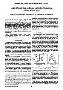
design. As a result, the power consumption is reduced mainly due to lower load capacitance on the clock bus, not only when the input logic is active but also when the input logic is held to zero. This paper is organized as follows. In Section II, the conventional TSPC-based design is reviewed and the low power scheme is proposed. Section III provides simulation results and performance comparisons. Section VI presents a conclusion. 2 Low-power TSPC-Based Domino Logic The TPSC-based domino logic scheme is proposed by Y. Ji-Ren et al. [4] as shown in Fig. 1, which uses three clock transistors. In this gate, the dynamic node Z is precharged high and M6 is disabled during precharge phase. As a result, the output F holds its previous value during the precharge phase and the precharge signal cannot be propagated to the output node, leading to a precharge noise reduction. However, the TSPC design suffers from large power consumption due to the requirement of 3 clock transistors per unit.
Figure 1: Conventional TSPC-based domino logic circuit.
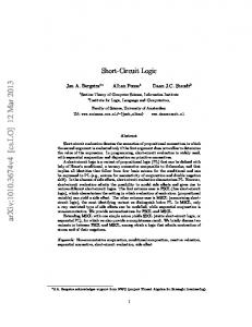
The proposed low-power TSPC-based domino logic circuit is shown in Fig. 2. In the proposed circuit, the source of the NMOS transistor M5 is connected to node B. As a result, the NMOS clock transistor in the second stage is removed as compared to the conventional TSPC-based scheme shown in Fig. 1. For our proposed gate, when the input logic A is low, the output node F is always kept low regardless of the operating phase. On the other hand, if the input A is high, the precharge and evaluation phases will lead to the following situation: • •
During the evaluation phase, node Z is discharged to Gnd as well as node B, resulting in enabling the PMOS transistor M4, while pulling up the output F to Vdd. During the precharge phase, node Z is charged up to Vdd, followed by the voltage at node B. Since the NMOS evaluation transistor M2 is disabled, the output node Z is held high (same value as the previous evaluation phase).
1169
1170
Fang Tang and Amine Bermak\ / Energy Procedia 14 (2012) 1168 – 1174 Author name / Energy Procedia 00 (2011) 000–000
Figure 2: The proposed domino logic circuit unit.
It should be mentioned that, a voltage drop Vpp at the output node F is existed, mainly due to charge sharing, which will be discussed later. Obviously, according to the timing diagram, the logic functionality of the proposed scheme is similar to the conventional TSPC-based domino logic circuit. A domino logic chain consists of alternative N-type and P-type modules. The proposed domino logic is also valid for the P-type domino logic. Similar to the N-type design, the source of the PMOS transistor M4 is connected to the drain of the PMOS evaluation transistor M1.
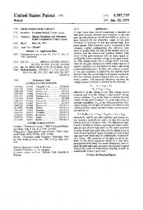
Figure 3: The keeper simulation waveforms. (A) the clock signal; (B) the input logic; (C) the output signal of the conventional TSPC-based domino logic without a keeper design; (D) the output signal of the proposed domino logic without a keeper design; (E) the output signal of the proposed domino logic with a keeper design.
3
4
1171
Fang Tang and Amine Bermak\ / Energy Procedia 14 (2012) 1168 – 1174 Author name / Energy Procedia 00 (2011) 000–000
Similarly to any dynamic logic circuits, the proposed scheme also suffers from charge sharing during the precharge phase. This charge sharing is mainly introduced by the parasitic capacitance at node B. This voltage drop at the output node could be propagated to the next stage and causes more serious charge sharing problems requiring special attention. The potential solution relies on using a keeper transistor together with an inverter [5]. Compared to the other solutions such as dual supply or transistor sizing techniques, the keeper-based solution is potentially interesting as there is no static short circuit current consumed and the voltage drop at the output node can be completely eliminated without the requirement of large parasitic capacitance. Simulation results related to the keeper design is shown in Fig. 3. Obviously, both the proposed scheme and the conventional TSPC-based domino logic suffer from charge sharing and after adding a keeper at the output node, the charge sharing can be eliminated. 3 Power Consumption Comparison In the proposed domino logic, the precharge pulse is prevented from propagating to the output node of the buffer resulting in a decreasing current consumption in the output stage of the domino gate. The total power consumed in the domino gate can be divided into two parts: (i) Pavg1 power consumed in the input stage of the gate (dynamic part) and ii) Pavg2 power consumed by the static buffer (second stage of the gate). The power dissipated in the first stage of the conventional domino logic can be expressed as: Pavg1=k.f.Vdd2.Cp + r.f.Vdd.Vpp.Cp
(1)
Where, f is the clock frequency, k is the input activity factor and r is the probability of the input being high (can be seen as the average duty cycle of the input logic). If A is held high, then transition probability k is zero, while the probability of input r being high is 100%. Cp is the equivalent internal parasitic capacitance of the first stage, including not only CZ, CB, but also those gate capacitances Cgs and Cgd of M1, M2, M4, M5. Vpp is the voltage change on these parasitic capacitances during the precharge phase. Eq. 1 shows that the power consumption of the first stage depends on the input logic activity k. Obviously, each time the input logic changes, these parasitic capacitances could be charged (or discharged). Besides the power dissipation due to the input logic activity, another important part of power is consumed during the precharge phase when the input logic is '1'. In this situation, the floating capacitance would be charged (or discharged) even at the clock rate f. Obviously, this part of the power is weighted by a factor r expressing the probability of the input being high during the precharge phase. The second component of the power is related to the one consumed in the second stage (Static inverter), which can be approximated as: Pavg2 = k.f.Vdd2 .(CLoad + Cbuf ) +r.f.Vdd.Vpp(CLoad+Cbuf)
(2)
Where, Cbuf is the internal parasitic capacitance of the buffer. If the load capacitance CLoad >> Cbuf, then equation (2) can be approximated as: Pavg2=k.f.Vdd2.CLoad+r.f.Vdd.Vpp.CLoad
(3)
Hence, the total power consumption of the conventional domino logic is expressed by adding Eq. 1 and Eq. 3: Ptot = k.f.Vdd2 .(CLoad + Cp ) +r.f.Vdd.Vpp(CLoad+Cp)
(4)
1172
Fang Tang and Amine Bermak\ / Energy 14 (2012) 1168 – 1174 Author name / Energy Procedia 00Procedia (2011) 000–000
5
The power consumption for the proposed PDB-based domino logic can be similarly estimated. In fact, the power consumption equation of the first stage is exactly the same as Eq. 1. However, the power consumed by the second stage can be now defined as: Pavg2=k.f.Vdd2.CLoad+r.f.Vdd.Vpp.CLoad
(5)
Where, Vpp is the voltage drop at the output node F during the precharge phase, due to the precharge pulse propagation. The total power saving is easily derived from Eq. 1, 4 and 5: = =
Ptot Ptot Ptot r.f.(Vpp Vpp).CLoad k.f.Vdd .(Cp + CLoad ) + r.f.Vpp .(Cp + CLoad )
(6)
Note from Eq. 6 that if we assume the input logic activity is very low (r >> k), then Eq. 6 can be approximated as:
(VppVpp)CLoad Vpp(Cp+CLoad)
(7)
Furthermore, if the propagated precharge pulse of the proposed domino logic Vpp is much smaller than Vpp, then the power saving could be further simplified as shown in Eq. 8. It is clear from Eq. 8 that the proposed Domino gate enables greater power saving for larger loading conditions.
CLoad Cp+CLoad
(8)
In practice, the frequency of the input signal A is generally high for dynamic logic circuit, thus the assumption r >> k is not always valid. If k is less than 50%, then Eq. 6 can be derived as follows: > =
1/2.f.(Vpp Vpp).CLoad 1/2.f.Vdd .(Cp + CLoad ) + 1/2.f.Vpp .(Cp + CLoad ) (Vpp Vpp).CLoad (Vdd + Vpp )(Cp + CLoad ) Vpp .CLoad (Vdd + Vpp)(Cp + CLoad )
Vpp