Organic Non-volatile Memory Devices Based on a Ferroelectric Polymer
2 l l R. Kalbitz , P. Friibing , R. Gerhard , D. M. Taylor l
I
�otsdam, Ge�any;.2School of
Dept. of Physics and Astronomy, University of Potsdam, Karl-Liebknecht-Str. 24-25, 14476,
Electronic Engineering, Bangor University, Dean Street, Bangor Gwynedd LL57 1UT, UK. Email:
[email protected]
Abstract-Organic based FeFETs have been studied using current voltage measurements. Evidence is presented supporting the idea that, during the application of a sequence of poling cycles, electrons
become
permanently
insulator/semiconductor
interface
fixed
probably
at
trapped
the on
the
positively charged surfaces of ferroelectrically polarized poly(vi
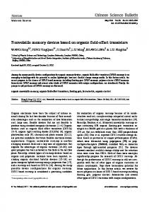
electrodes are both grounded, the device is effectively in the OFF state (no accumulation channel is formed). Negative voltages applied to the source (S) should only give rise, therefore, to a parasitic hole current from the drain through the bulk semiconductor to the source. Pl, P3, PS, ..., P29
nylidenefluoride-trifluoroethylene) (P(VDF-TrFE» crystalites at the interface.
P2, P4, P6, ..., P30
II
II
In recent years, ferroelectric field-effect transistors (FeFET) based on the ferroelectric co-polymer polyvinylidene fluoride terfluoroethylene, P(VDF-TrFE), have been studied by Reece et al.[I], Naber et al.[2, 3, 4] and others.[5, 6, 7] The
ferroelectric properties of spin-cast P(VDF-TrFE) films make this material a good candidate for applications.
Although
Naber
et
non-volatile al.[4]
memory
suggested
that
depolarization of the ferroelectric domains occurred under depletion voltages, strong evidence has been found that the ferroelectric insulator remains in a stable polarized state.[8] Instead of depolarization it was demonstrated in measurements on metal-insulator-semiconductor (MIS) capacitors[8, 9] that fixed negative charges at the semiconductor/insulator interface compensate the ferroelectric polarization. This compensation may serve as a plausible explanation for the FeFET device instability under depletion voltages. Such an instability may consequently
lead
to
reduced
data
retention
times
and
therefore need to be studied more closely. To date, it is not clear whether these negative compensation charges become trapped during operation, i.e the application of a gate (G) voltage to the MIS structure. To answer this question
measurements
on
application of the voltage trapping
of
structurally
FeFETs
were
preformed
by
pattern shown in Fig. 1. The
fixed
negative
charges
at
the
semiconductor-insulator interface is expected to lead to an increased current between source (S) and (D), Is, which can be measured independently of the gate current. The studied FeFET devices were based on poly(3-hexylthiopene) (P3HT) as the semiconductor and P(VDF-TrFE) as the gate insulator with film thicknesses of 0.05 /-LID and 0.3 /-LID respectively. FET
characteristics
were
measured
under
a
nitrogen
atmosphere with an Agilent 4155C Semiconductor Parameter Analyzer from Hewlett Packard. The change in Is under accumulation and depletion voltages during the first poling cycles was measured with the unipolar/bipolar voltage pattern depicted in Fig. 1. The successive unipolar loops, denoted C1 and C2, make it possible to identify influences arising from the reorientation of the molecular dipoles on Is as well as on the gate current, IG. During negative bipolar half-cycles, labeled PI, P3, ... in Fig. 1, since the drain (D) and gate (G)
978-1-4577-1025-4/11/$26.00 ©2011 IEEE
Figure I: Poling procedure used for the measurement of the out�ut characteristics. Negative/positive voltages correspond to depeletlOn/ accumulation of the device. Each bipolarcycle is labeled
as
PI, P2 et cetera.
Odd (PI,P3,... )and even numbers (P2,P4,... )correspond to negative and positive voltages respectively applied to the right hand contact to the semiconductor.
Consequently,
only
a
small,
negative Is should
be
measured. For positive half-cycles, labeled P2, P4... P30, the device is effectively connected in the saturation mode (fully ON). When positively biased, the right-hand electrode now acts as the source of holes for the p-type accumulation channel formed at the semiconductor-insulator interface, leading to large positive Is. A selection of output characteristics for negative and positive voltages is given in Fig. 2(a) and 3(a), respectively. In these data sets, device currents were measured as a function of the unipolar/bipolar source voltage cycles (see Fig. 1) with the poling direction reversed thirty times. The sequence started with a negative poling voltage PI, followed by positive poling P2 and so forth. In Fig. 2(a), Is is seen to increase with the number of poling cycles. During the first cycle (PI), Is increases to 7
�
10-7 A when VDS
=
-40 V.
During subsequent poling steps Is increases rapidly eventually saturating at
�
5 x 10⁻⁶ A after passing through a maximum
at lower voltages. The corresponding gate currents, given in Fig. 2(b), show a clear
current
peak
of
�
2 x 10⁻⁷ A
associated
with
ferroelectric switching superimposed on a much smaller leakage current. Therefore, the larger peaks in Is observed during sequential poling cycles PI to P29 must be caused by an increase of conductivity at the semiconductor-interface and is the result of a shift in the threshold voltage of the device rather than from gate-source current flow.
- 207 -
The output characteristics at accumulation voltages, given
This increase in conductivity appears to be irreversible and provides
strong
evidence
negative
charges
during
for the the
fIrst
interfacial poling
trapping
cycles.[8]
of
in Fig. 3(a), also show saturation behavior. However, the
The
increase of Is during poling cycles P2 to P30 is not as strong
presence of such charges will promote the accumulation of
as in Fig.
holes at the semiconductor-insulator interface leading to an
measurement
increase in Is at depletion voltages.
(evidenced by the peak in gate current in Fig. 3(b» has only a
2(a). Furthermore, the currents observed in this regime,
show
that
ferroelectric
switching
minor effect on the conductivity of the accumulation channel between source and drain.
(a)