The physical design tools we developed for 3D FPGAs build on those proposed ... channel segments. programmed gate arrays, semi- and full custom ICs). This.
Placement and Routing for Three-Dimensional FPGAs � Michael J. Alexander, James P. Cohoon, Jared L. Col esh, John Karro, Edward L. Peters and Gabriel Robins Department of Computer Science, University of Virginia, Charlottesville, VA 22903
Abstract
We explore physical layout for a three-dimensional (3D) FPGA architecture. For placement, we introduce a topdown partitioning technique based on rectilinear Steiner trees; we then employ a one-step router to produce the nal layout. Experimental results indicate that our approach produces e�ective 3D layouts, using considerably shorter average interconnect distance than is achievable with conventional 2D FPGA's of comparable size.
1 Introduction
A eld-programmable gate array (FPGA) is a exible and reusable design alternative to custom integrated circuits. Using FPGAs, digital designs can be quickly implemented and emulated in hardware, which enables a faster, more economical design cycle [8]. The exible logic and connection resources of FPGAs allow di�erent designs to be implemented on the same hardware. However, this versatility comes at the expense of a substantial performance penalty due primarily to signal delay through the programmable routing switches. This delay can account for over 70% of the clock cycle period [19, 25]. This paper explores physical-design issues for a new three-dimensional (3D) FPGA architecture, with a focus on reducing the interconnect delay. The increased number of switch block neighbors in our new architecture (i.e., 6 in 3D vs. 4 in 2D) a�ords greater exibility during placement and routing, while shorter average interconnect distance (i.e., O(n 31 ) for an n-block 3D FPGA vs. O(n 21 ) in 2D) implies shorter signal propagation delays. In order to realize such potential bene ts, we must develop e�ective physical-design techniques which exploit these properties. The physical design tools we developed for 3D FPGAs build on those proposed in [4], and adapt these technique for the new architecture. Our placement algorithm employs a top-down approach: the FPGA is partitioned into several cubic sections, logic blocks are arranged to minimize the number of nets crossing partition boundaries, and each partition is similarly processed in a recursive � Professor Cohoon is supported by NSF grants CCR{9224789 and MIP{9107717. Professor Robins is supported by NSF Young Investigator Award MIP-9457412 and by a Packard Foundation Fellowship. Our benchmarks and additional related papers may be found at WWW URL http://www.cs.virginia.edu/~vlsicad/
manner. We use a one-step graph-based router which employs a Steiner-based heuristic to construct the overall routing solution. Our benchmarks indicate that our three-dimensional layout algorithms generate 23% average savings in total interconnect length over traditional 2-OPT -based placements. In addition, our three-dimensional layout reduces average interconnect distance by 14% and average maximum source-sink path length by 26%, with respect to 2-OPT -based placements. The remainder of the paper is organized as follows: In Section 2 we discuss our 2D and 3D FPGA architecture models, and address some of the physical constraints in constructing our 3D variant. In Section 3 we discuss performance gains expected for the 3D architecture. Sections 4 and 5 present our physical layout techniques for 3D placement and routing, respectively. Section 6 contains experimental results for 3D FPGAs and compares these results with those achievable for 2D FPGAs, and we conclude in Section 7.
2 The FPGA Architecture
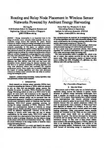
Field-programmable gate arrays are reprogrammable chips capable of implementing arbitrary design logic. The basic 2D FPGA architecture consists of a symmetrical array of user-con gurable logic blocks. Running through the channels between the rows and columns of logic blocks is a network of channel segments, linked together by programmable switch blocks [8] (Figure 1). During customization, con guration data is downloaded onto an FPGA, specifying which programmable switches are to be made active (i.e., programmed \ON"). This process causes each net (i.e., a set of logic-block input/output pins) to be properly interconnected. Our 3D FPGA architecture [2] is a generalization of the basic 2D model, in which each switch block has six immediate neighbors (Figure 2(a)), as opposed to four in 2D. Three-dimensional switch blocks are analogous to their two-dimensional counterparts; they enable each channel segment to connect to some subset of the channel segments incident on the other ve faces of the 3D switch block (Figure 2(b)). Although the usable-gate count of FPGAs has been steadily increasing, the number of usable gates in FPGAs is signi cantly less than in other design styles (mask-
Channel Segment
Logic Blocks
Switch Block
Figure 1: Two-dimmensional FPGA architecture.
An alternative approach investigates the use of optical interconnect to construct multi-layered FPGAs [10]. I/O for individual FPGA chips was recently enhanced by using solder bumps distributed across the FPGA die [26]. The three-dimensional FPGA model poses a number of new challenges in the area of heat dissipation. Higher operating temperatures can lead to less reliable operation (e.g., heat stress can induce faults). A number of MCM thermal-dissipation techniques (e.g., thermal bumps and pillars [9], thermal gels [7], etc.) may also be applicable to 3D FPGAs. Chip-size packages [23, 28] are a relatively new packaging technology which results in a package typically only 10% larger than the bare die itself. One such package consists of a thin epoxy coating, which allows bonding pads to be placed directly over the die surface. An important bene t of chip-sized packages is the reduction of thermal stress by physical bu�ering of the die. A second motivation for using chip-sized packages rather than bare dies is the known-good-die problem: compared to packaged die, testing of bare dies is costly as well as time-consuming. Chip-size packages, which are essentially testable dies, can dramatically reduce this problem [14].
3 Reducing Interconnect Length
(a)
(b)
Figure 2: (a) Arrangement of switch blocks in 3D FPGA, and (b) detail of 3D switch block. Dark lines in (a) denote channels containing parallel channel segments.
programmed gate arrays, semi- and full custom ICs). This reduction in gate count is an inevitable consequence of the additional chip area dedicated to programmable routing switches and SRAM-based con guration data for these switches [24]. More recent FPGA architectures [27] strive to increase usable-gate-counts by reducing the number of programmable switches. Three-dimensional VLSI has recently begun to attract increased attention. The implications of threedimensional abutment of individual transistors has been studied in [16]. Issues in vertical integration have been investigated in [1], with a focus on \silicon-on-insulator" techniques. In order to reduce delay between individual FPGAs, [11] proposed adding a surrounding programmable interconnection frame to individual die, using an MCM substrate for interconnections between frames.
In this section, we explore analytically both the expected interconnect length and the required number of programmable switches. Channel segments on an FPGA are linked together with programmable switches. Under our 2D and 3D architecture models, reducing the interconnect length also reduces the number of programmable switches encountered along the traversed interconnect (which further lowers the interconnect delay). Consider two FPGA architectures, each having n switch blocks, arranged in a 2D grid and in a 3D grid (Figure 2(a)). The expected distance between two uniformly distributed points in the unit interval is 31 , and therefore the expected Manhattan distances between two uniformly2 distributed points in the unit square and unit cube are 3 and 33 = 1, respectively. Thus, the expected interconnect length for a two-pin net in an FPGA of n switch blocks, is 32 � n 12 and n 13 in 2D and 3D, respectively. Equating the average interconnect length values in the di�erent architectures and solving for a break-even value of n indicates that the average interconnect length is expected to be shorter in 3D than in 2D when n � 12. Because typical values of n in existing FPGA parts already far surpass this value, we can expect 3D interconnect lengths to be shorter than their 2D counterparts. Currently available parts contain over 500 switch blocks [27]; for n = 525, the expected average interconnect length in three dimensions is less than half its value in two dimensions.
the FPGA. Finally, during routing, nets are electrically interconnected using the available routing resources. PROGRAMMED PROGRAMMED "ON" Minimizing signal delay is an important consideration "ON" during these physical layout phases. In order to miniROUTE mize delay for each net, source-sink path lengths should ROUTE be minimized. To minimize the FPGA size required to imPROGRAMMED PROGRAMMED plement a design (or equivalently, to insure that a given "OFF" "OFF" piece of the design ts onto a single FPGA), we must also (UNAVAILABLE) (UNAVAILABLE) minimize the maximum number of channel segments as(a) (b) signed to nets over all channels (this is commonly referred to as reducing congestion). Traditionally, these phases of layout have been considFigure 3: (a) 2D switch block with fanout 3, and ered independently and performed sequentially. Since the (b) 3D switch block with fanout 5. quality of the results of any one phase depends on results from earlier phases, it is bene cial for each phase to consider its e�ects on subsequent phases. A placement technique called Mondrian was designed to speci cally conA popular 2D switch-block architecture [27] allows each sider the e�ects of placement on routing for 2D FPGAs [4] incoming channel segment to connect to a single segment [13]. Here we generalize this method to three dimensions. on the other three sides, providing a fanout of F 2 = 3. Our 3D FPGA placement algorithm uses a recursive Our 3D architecture generalizes this switch-block scheme geometric technique called thumbnail partitioning, which to three dimensions, resulting in a fanout of F 3 = 5. decomposes the FPGA area into an m � n � r grid. In When a route passes through a switch block, all of the our case, m = n = 3 (and r = 1) for a standard twofanout channel segments (either three or ve) become un- dimensional FPGA, and m = n = r = 2 for the threeavailable to subsequent nets; one or more of the fanout dimensional FPGA shown in Figure 4. segments is committed to the route by being programmed \ON" to make the connection, while the remaining fanout segments become unusable (they must be programmed \OFF" to ensure that subsequent nets are electrically disjoint (Figure 3) from the current net). Thus, while interconnections in the 3D con guration are shorter, they commit more switching hardware per unit length. This motivates a more re ned analysis as follows: (cost per unit len 2D) (cost per unit len 3D) �(expected len 2D) = �(expected len 3D) F 2 � 32 � n 12 = F 3 � n 13 Figure 4: (a) Partition template with m = n = r = 2, and (b) partitioning graph where partitionn = 244 template regions correspond to nodes. Thus, an average net is expected to use fewer switching resources when routed in three dimensions for n � 244 switch blocks (this size range applies to most currently manufactured parts). Hardware requirements re- The placement phase overlays the FPGA with a partimain greater in three dimensions: however, if channel tioning template, partitioning the overall design logic into widths can be reduced su�ciently by going to three dimen- m � n � r regions. Cut-lines of the template pass through sions, then identical circuits may be implemented with less switch blocks, so each logic block lies entirely within a sinoverall hardware using a three-dimensional FPGA part. gle region of the partitioning template. The distribution of logic blocks among regions of the partitioning template 4 Three-Dimensional FPGA Placement is then improved using simulated annealing [20], where a FPGA layout is generally performed in three phases: move consists of swapping pairs of logic blocks from di�erregions of the partitioning template, with the objective (1) technology mapping, (2) placement, and (3) rout- ent being minimizing total interconnect length over all nets. ing. During technology-mapping, the design logic is partitioned into small \units", each capable of being imple- For each net, we consider the set of partitions in which mented by an individual logic block. During placement, that net has been placed, and we calculate the minithese units are each assigned to speci c logic blocks on mum rectilinear Steiner tree connecting these points (i.e., s; D
s; D
s; D
s; D
the thumbnail). An important measure of the quality of a placement and global routing is maximum congestion, which in our case is the number of thumbnail edges crossing any given cut-line. Once logic blocks have been assigned to regions in the partitioning template, a congestion-balancing step is undertaken. Note that a typical set of partitions can have many `thumbnails (see Figure 5). The objective of the congestion-balancing step is to assign one of the possible thumbnail alternatives to each net in a manner that minimizes the maximum number of thumbnails having edges that cross the same cut-line of the partitioning template. Since this problem is NPcomplete [13], it is accomplished using a greedy heuristic.
(b)
(a)
Figure 6: A section of the routing graph showing (a) a 3D FPGA switch box, and (b) the corresponding portion of the routing graph. G = (V; E), where V is the node set and E � V � V is a set of weighted edges, we must span a subset of the nodes N � V (i.e., the net), while the remaining nodes may be used as Steiner points. Each edge e 2 E has a weight w corresponding to interconnect distance, and our goal is to minimize the total spanning cost. The graph Steiner problem is formally de ned as follows: ij
ij
Figure 5: Three possible thumbnails for interconnecting the four dark-shaded nodes shown. Unshaded nodes represent possible Steiner nodes.
The Graph Steiner Minimum Tree (GSMT) problem: Given a weighted graph G = (V; E) and a net of terminals N � V to interconnect, nd a treePT = (V ; E ) with N � V � V and E � E such that w is 0
Next, every edge in each thumbnail must be assigned to a speci c switch block along the crossed cut-line of the partitioning template. Each such switch block is conceptually added as a new \virtual" pin in the net. The portion of each net within each region of the partitioning template is then passed on to a lower level of the recursion (this is akin to the virtual terminal [6] and terminal propagation [12] techniques). Assignments are made using a minimum-bipartite-matching heuristic, where one set of nodes represent all nets crossing a cut-line, and the other node set represents the switch boxes on that cut-line. The recursion terminates when a region contains at most one logic block. Minimizing thumbnails for each net while balancing overall congestion produces routable placements.
5 Three-Dimensional FPGA Routing
After the placement phase, all portions of the design logic have been assigned to speci c logic blocks on the FPGA. It is now the task of the router to interconnect the pins of each net. The routing phase models the FPGA as a graph, where the overall graph topology mirrors the complete FPGA architecture. Paths in this graph correspond to feasible routes on the FPGA, and conversely (See Figure 6). Nets are routed one at a time, using a move-to-front heuristic when infeasibility is encountered. Routing each net on the FPGA corresponds to the graph version of the Steiner problem: given a graph
0
0
eij 2E 0
0
0
ij
minimized. The GSMT problem is NP-complete [17]; we therefore employ the Iterated-KMB (IKMB) heuristic of [3] and adapt it to routing in three dimensions. The IKMB algorithm in turn uses the heuristic of [21] (which we call \KMB") to e�ciently search for solutions of increasing quality. Given a graph G = (V; E), the net N � V , and a set S of potential Steiner points, we de ne the following: �KMB (N; S) = KMB (N) ? KMB (N [ S) G
G
G
The IKMB algorithm starts by computing the KMB tree. Then, at each iteration the IKMB method repeatedly nds additional Steiner node candidates that reduce the overall KMB cost and includes them into the growing set of Steiner nodes S (see Figure 8). The cost of the KMB tree over N [ S will decrease with each added node, and the construction terminates when there is no x 2 V with �KMB(N [ S; fxg) > 0. The IKMB method is formally described in Figure 7. The IKMB algorithm mirrors the Iterated 1-Steiner method [15] [18] and is quite e�ective in reducing total interconnect length for 2D FPGAs [5]. Our experimental results indicate that IKMB is also e�ective for 3D FPGAs (see Section 6). Figure 8 shows how introducing Steiner points into the routing solution can reduce total interconnect length.
Circuit Name 9symml 2large alu2 apex7 example2 term1
Placement algorithm Mondrian Mondrian Mondrian Mondrian Mondrian Mondrian Totals: 9symml Mondrian + 2-OPT-PAIR 2large Mondrian + 2-OPT-PAIR alu2 Mondrian + 2-OPT-PAIR apex7 Mondrian + 2-OPT-PAIR example2 Mondrian + 2-OPT-PAIR term1 Mondrian + 2-OPT-PAIR Totals: 9symml Mondrian + 2-OPT-FIRST-a 2large Mondrian + 2-OPT-FIRST-a alu2 Mondrian + 2-OPT-FIRST-a apex7 Mondrian + 2-OPT-FIRST-a example2 Mondrian + 2-OPT-FIRST-a term1 Mondrian + 2-OPT-FIRST-a Totals: 9symml Mondrian + 2-OPT-FIRST-b 2large Mondrian + 2-OPT-FIRST-b alu2 Mondrian + 2-OPT-FIRST-b apex7 Mondrian + 2-OPT-FIRST-b example2 Mondrian + 2-OPT-FIRST-b term1 Mondrian + 2-OPT-FIRST-b Totals:
Overall Totals:
Total Interconnect Random Mondrian 1057 627 2481 1462 2143 1533 1468 737 2286 1624 1119 447 10554 6430 857 661 2195 1464 1936 1533 1400 741 2040 1597 829 450 9257 6446 606 583 1479 1412 1290 1282 735 726 1270 1265 479 452 5859 5720 606 583 1479 1412 1290 1282 797 713 1270 1265 479 452 5921 5707
31591
�% 40.7 41.1 28.5 49.8 29.0 60.1 39.1 22.9 33.3 20.8 47.1 21.7 45.7 30.4 3.8 4.5 0.6 1.2 0.4 5.6 2.4 3.8 4.5 0.6 10.5 0.4 5.6 3.6
24303 23.1
Channel Width Random Mondrian 6 7 9 7 8 7 6 7 8 7 5 7 42 42 6 7 9 7 8 7 6 7 8 7 6 7 43 42 8 6 7 6 7 6 6 6 7 7 6 6 41 37 8 6 7 6 7 6 6 6 7 7 6 6 41 37
167
158
�% -16.7 22.2 12.5 -16.7 12.5 -40.0 0.0 -16.7 22.2 12.5 -16.7 12.5 -16.7 2.4 25.0 14.3 14.3 0.0 0.0 0.0 9.8 25.0 14.3 14.3 0.0 0.0 0.0 9.8
5.4
Table 1: The e�ects of three-dimensional Mondrian placement on total interconnect length and minimum channel width of several benchmark circuits. The percentages indicate the performance of Mondrian with respect to random placements (positive values indicate improvement, while negative percentages indicate disimprovement).
The Iterated-KMB (IKMB) Algorithm Input: A weighted graph G = (V; E) and net N � V Output: A low-cost tree spanning N S=; While C = fx 2 V ? N j�KMB (N [ S; fxg) > 0g 6= ; Do Find x 2 C with maximum �KMB (N [ S; fxg) S = S [ fxg Return KMB (N [ S) G
G
G
Figure 7: Iterated-KMB algorithm (IKMB).
6 Experimental Results
Our placement and routing algorithms were implemented using C++ in the SUN Unix environment. We considered 6 large industrial benchmark circuits frequently used to evaluate FPGA routers [22]. Each circuit was rst placed using the Mondrian method, and then the placement was further re ned using a 2-OPT post-processing step. The various 2-OPT methods we used were as follows: (i) 2-OPT-PAIR, which starts by making the best swap possible, and then \follows" those two blocks, making any bene cial swap involving one of them; (ii) 2-OPT-FIRST-a, which makes the rst bene cial swap found, and continues to do so until the number of swaps made exceeds the square of the number of blocks; and (iii) 2-OPT-FIRST-b, which is similar to 2-OPT-FIRST-a but runs until no possible swap would result in a savings of more than 1%. For comparison purposes, we also tested our tool on random placements (postprocessed by greedily swapping pairs of blocks). Thus, we
nique based on optimal rectilinear Steiner trees, and for routing we developed a graph-based one-step router to produce a nal layout. Our experimental results indicate that our approach produces e�ective 3D layouts, using considerably less interconnect than is required with conventional 2D FPGAs of comparable size.
References
(a)
(b)
Figure 8: Example of routing solutions for a single 3-pin net (dark blocks represent pins), produced by (a) the KMB algorithm, and (b) the IKMB algorithm. The shaded switch block in (b) serves as a Steiner point to reduce overall interconnect length by about 16% in this case.
[1] Y. Akasaka, Three-Dimensional IC Trends, Proc. IEEE, 74 (1986), pp. 1703{1714. [2] M. J. Alexander, J. P. Cohoon, J. L. Coleflesh, J. Karro, and G. Robins, Three-Dimensional FieldProgrammable Gate Arrays, in Proc. IEEE Intl. ASIC Conf., Austin, TX, September 1995, pp. 253{256. [3] M. J. Alexander, J. P. Cohoon, J. L. Ganley, and G. Robins, An Architecture-Independent Approach to FPGA Routing Based on Multi-Weighted Graphs, in Proc. European Design Automation Conf., Grenoble, France, September 1994, pp. 259{264. [4] M. J. Alexander, J. P. Cohoon, J. L. Ganley, and G. Robins, Performance-Oriented Placement and Routing for Field-Programmable Gate Arrays, in Proc. European Design Automation Conf., Brighton, England, September 1995, pp. 80{85. [5] M. J. Alexander and G. Robins, New PerformanceDriven FPGA Routing Algorithms, in Proc. ACM/IEEE Design Automation Conf., San Francisco, CA, June 1995, pp. 562{567. [6] S. Bapat and J. P. Cohoon, A Parallel VLSI Circuit Layout Methodology, in Proc. IEEE Intl. Conf. VLSI Design, January 1993, pp. 236{241. [7] D. M. Brewer and L. P. Burnett, MCM Designs Require Exhaustive Thermal Analysis, Electronic Design News, (1992), pp. 96{103. [8] S. D. Brown, R. J. Francis, J. Rose, and Z. G. Vranesic, Field-Programmable Gate Arrays, Kluwer Academic Publishers, Boston, MA, 1992. [9] P. C. Chan, Design Automation for Multichip Modules { Issues and Status, Intl. J. of High Speed Electronics, 2 (1991), pp. 236{285. [10] J. Depreitere, H. Neefs, H. V. Marck, J. V.
benchmarked eight types of placements: (i) random, (ii) random followed by (three distinct kinds of) 2-OPT postprocessing , (iii) Mondrian, and (iv) Mondrian followed by (three distinct kinds of) 2-OPT post-processing. Table 1 shows the total interconnect length and the minimum channel width for each benchmark circuit. The results indicate that our placement algorithm generated 23:1% savings in total interconnect length over random placements. The overall improvement in minimum channel widths is 5:4%. Our Mondrian placement algorithm tends to draw logic blocks closer together, thus minimizing total interconnect length (in certain cases, this can increase the minimum channel width required to route the circuit). Table 2 shows the average interconnect length per net, the average number of programmable switches required to route a net, and the average maximum source-sink pathlength (i.e., radius). As expected from the analysis in Section 3, the increased switching exibility in three dimensions decreases all of these values. Our results indicate a reduction of 13:8% in average interconnect length, 23:0% savings in average switch block usage, and 26:4% reducCampenhout, B. D. R. Baets, H. Thienpont, and tion in average source-sink path-length. These results are I. Veretennicoff, An Optoelectronic 3-D Field Proencouraging with respect to interconnect delay minimizagrammable Gate Array, in Proc. 4th Intl. Workshop tion in three-dimensional FPGAs (as compared to their on Field-Programmable Logic and Applications, Prague, two-dimensional counterparts). Figure 9(a) illustrates a September 1994. 2D layout of one of the benchmark circuits (ALU2), while Figure 9(b) shows the layout of the same circuit on a 3D [11] I. Dobbelaere, A. E. Gamal, D. How, and B. KleveFPGA. land, Field Programmable MCM Systems { Design of an Interconnection Frame, in Custom Integrated Circuits Conf., Boston, MA, 1992, pp. 4.6.1{4.6.4. We have presented an e�ective physical layout frame- [12] A. E. Dunlop and B. W. Kernighan, A Procedure for Placement of Standard-Cell VLSI Circuits, IEEE Trans. work for a new three-dimensional FPGA architecture. For Computer-Aided Design, 4 (1985), pp. 92{98. placement, we have used a top-down partitioning tech-
7 Conclusions
[13] J. L. Ganley, Geometric Interconnection and Placement Algorithms, PhD thesis, Department of Computer Science, University of Virginia, Charlottesville, Virginia, 1995. [14] L. Gilg, Known Good Die Meets Chip Size Package, IEEE Circuits and Devices Magazine, (1995), pp. 32{37. [15] J. Griffith, G. Robins, J. S. Salowe, and T. Zhang, Closing the Gap: Near-Optimal Steiner Trees in Polynomial Time, IEEE Trans. Computer-Aided Design, 13 (1994), pp. 1351{1365. [16] A. C. Harter, Three-Dimensional Integrated Circuit Layout, Cambridge University Press, New York, 1991. [17] F. K. Hwang, D. S. Richards, and P. Winter, The Steiner Tree Problem, North-Holland, 1992. [18] A. B. Kahng and G. Robins, A New Class of Iterative Steiner Tree Heuristics With Good Performance, IEEE Trans. Computer-Aided Design, 11 (1992), pp. 893{902. [19] A. B. Kahng and G. Robins, On Optimal Interconnections for VLSI, Kluwer Academic Publishers, Boston, MA, 1995. [20] S. Kirkpatrick, C. D. Gelatt, and M. P. Vecchi, Optimization by Simulated Annealing: An Experimental Evaluation (part 1), Science, 220 (1983), pp. 671{680. [21] L. Kou, G. Markowsky, and L. Berman, A Fast Algorithm for Steiner Trees, Acta Informatica, 15 (1981), pp. 141{145. [22] G. G. Lemieux and S. D. Brown, A Detailed Routing Algorithm for Allocating Wire Segments in FieldProgrammable Gate Arrays, in Proc. ACM/SIGDA Physical Design Workshop, Lake Arrowhead, CA, April 1993. [23] D. Maliniak, Chip-Scale Packages Bridge the Gap Between Bare Die and BGAs, Electronic Design, (1995), pp. 65{73. [24] J. Rose, R. J. Francis, D. Lewis, and P. Chow, Architecture of Field-Programmable Gate Arrays: The E�ect of Logic Block Functionality on Area E�ciency, IEEE J. Solid State Circuits, 25 (1990), pp. 1217{1225. [25] S. M. Trimberger, Field-Programmable Gate Array Technology, S. M. Trimberger, editor, Kluwer Academic Publishers, Boston, MA, 1994. [26] J. R. V. Maheshwari, J. Darnauer and W. W.-M. Dai, Design of FPGAs with Area I/O for Field Programmable MCM, in Proc. ACM/SIGDA Intl. Symposium on Field-Programmable Gate Arrays, 1995. [27] Xilinx, The Programmable Gate Array Data Book, Xilinx, Inc., San Jose, California, 1994. [28] M. Yasunaga, S. Baba, M. Matsuo, H. Matsushima, S. Nakao, and T. Tachikawa, Chip Scale Packages: \A Lightly dressed LSI Chip", IEEE Trans. on Components, Packaging and and Manufacturing Tech., 18 (1995), pp. 451{457.
(a)
(b) Figure 9: Final layout of circuit ALU2 on (a) 16 � 16 2D FPGA, and on (b) 4 � 8 � 8 3D FPGA. Placement was done using Mondrian without 2OPT post-processing in both cases.
Circuit # Name Nets 9symml 79 2large 186 alu2 153 apex7 115 example2 205 term1 88 9symml 2large alu2 apex7 example2 term1
79 186 153 115 205 88
9symml 2large alu2 apex7 example2 term1
79 186 153 115 205 88
9symml 2large alu2 apex7 example2 term1
79 186 153 115 205 88
9symml 2large alu2 apex7 example2 term1
79 186 153 115 205 88
9symml 2large alu2 apex7 example2 term1
79 186 153 115 205 88
9symml 2large alu2 apex7 example2 term1
79 186 153 115 205 88
9symml 2large alu2 apex7 example2 term1
79 186 153 115 205 88
Placement algorithm Random Random Random Random Random Random
Averages: Random + 2-OPT-PAIR Random + 2-OPT-PAIR Random + 2-OPT-PAIR Random + 2-OPT-PAIR Random + 2-OPT-PAIR Random + 2-OPT-PAIR Averages: Random + 2-OPT-FIRST-a Random + 2-OPT-FIRST-a Random + 2-OPT-FIRST-a Random + 2-OPT-FIRST-a Random + 2-OPT-FIRST-a Random + 2-OPT-FIRST-a Averages: Random + 2-OPT-FIRST-b Random + 2-OPT-FIRST-b Random + 2-OPT-FIRST-b Random + 2-OPT-FIRST-b Random + 2-OPT-FIRST-b Random + 2-OPT-FIRST-b Averages: Mondrian Mondrian Mondrian Mondrian Mondrian Mondrian Averages: Mondrian + 2-OPT-PAIR Mondrian + 2-OPT-PAIR Mondrian + 2-OPT-PAIR Mondrian + 2-OPT-PAIR Mondrian + 2-OPT-PAIR Mondrian + 2-OPT-PAIR Averages: Mondrian + 2-OPT-FIRST-a Mondrian + 2-OPT-FIRST-a Mondrian + 2-OPT-FIRST-a Mondrian + 2-OPT-FIRST-a Mondrian + 2-OPT-FIRST-a Mondrian + 2-OPT-FIRST-a Averages: Mondrian + 2-OPT-FIRST-b Mondrian + 2-OPT-FIRST-b Mondrian + 2-OPT-FIRST-b Mondrian + 2-OPT-FIRST-b Mondrian + 2-OPT-FIRST-b Mondrian + 2-OPT-FIRST-b Averages:
Overall Averages:
Avg. 2D 18.9 19.7 20.8 20.0 16.8 18.5 19.1 13.3 18.2 19.4 19.2 13.8 13.2 16.2 8.9 10.5 10.6 7.9 6.9 6.0 8.5 8.9 10.5 10.6 8.1 6.9 6.0 8.5 11.0 9.9 10.8 10.6 7.1 7.2 9.4 11.0 9.6 10.8 10.5 7.3 7.2 9.4 8.8 8.7 9.3 7.9 6.3 5.8 7.8 8.8 8.7 9.3 9.3 6.3 6.2 8.1
Net Length 3D �% 13.4 29.1 13.3 32.4 14.0 32.6 12.8 36.3 11.2 33.6 12.7 31.4 12.9 32.5 10.9 18.5 11.8 35.0 12.7 34.8 12.2 36.4 10.0 27.8 9.4 28.7 11.2 30.9 7.7 14.2 7.9 24.2 8.4 20.7 6.4 19.2 6.2 10.3 5.4 8.6 7.0 17.6 7.7 14.2 7.9 24.2 8.4 20.7 6.9 14.1 6.2 10.3 5.4 8.6 7.1 16.5 7.9 27.9 7.9 20.9 10.0 7.1 6.4 39.3 7.9 -11.4 5.1 29.2 7.5 20.2 8.4 23.9 7.9 17.6 10.0 7.1 6.4 38.4 7.8 -7.4 5.1 29.2 7.6 19.1 7.4 15.9 7.6 12.7 8.4 10.0 6.3 19.8 6.2 1.5 5.1 12.1 6.8 12.8 7.4 15.9 7.6 12.7 8.4 10.0 6.2 33.3 6.2 1.5 5.1 17.2 6.8 19.1
10.9 8.4 13.8
Avg. # Switches 2D 3D �% 17.5 12.4 29.1 18.3 12.2 33.4 19.1 12.8 32.8 18.7 11.8 37.1 15.5 10.0 35.2 17.2 11.57 32.8 17.7 11.8 33.3 12.0 9.9 17.3 16.7 10.6 36.3 17.8 11.6 34.7 17.9 11.1 37.9 12.5 8.9 29.3 12.0 8.4 29.8 14.8 10.1 31.8 7.6 6.8 11.0 9.1 6.9 23.6 9.1 7.5 17.3 6.7 5.6 16.0 5.7 5.3 7.0 4.8 4.7 1.4 7.2 6.1 15.3 7.6 6.8 11.0 9.1 6.9 23.6 9.1 7.5 17.3 6.9 6.1 10.7 5.7 5.3 7.0 4.8 4.7 1.4 7.2 6.2 13.9 9.7 7.1 27.1 8.5 6.7 21.6 9.3 8.8 5.0 9.3 5.5 40.6 6.0 6.9 -15.9 6.0 4.2 29.9 8.1 6.5 19.8 9.7 7.4 23.6 8.2 6.8 17.1 9.3 8.9 4.9 9.2 5.5 39.8 6.1 6.8 -11.9 6.1 4.3 29.3 8.1 6.6 18.5 7.4 6.5 12.3 7.4 6.5 12.2 7.9 7.4 6.2 6.6 5.4 18.2 5.1 5.2 -1.7 4.7 4.2 11.3 6.5 5.9 9.2 7.4 6.5 12.3 7.4 6.5 12.2 7.9 7.4 6.2 8.0 5.2 34.6 5.1 5.2 -1.7 5.0 4.2 15.8 6.8 5.8 14.7
9.6
7.4 23.0
Avg. Radius 2D 3D �% 14.8 9.4 36.7 16.0 10.5 34.4 16.4 10.2 38.0 16.1 10.0 38.1 14.5 9.2 36.7 15.7 10.4 33.6 15.6 10.0 35.9 10.8 7.9 27.0 14.7 9.2 37.1 15.3 9.1 40.6 15.8 9.6 38.9 12.1 8.4 30.2 11.0 7.8 29.0 13.3 8.7 34.6 6.6 5.7 13.0 8.5 6.1 28.8 7.9 6.1 22.7 6.7 5.1 22.6 5.8 5.1 11.5 5.0 4.5 9.5 6.8 5.4 20.6 6.6 5.7 13.0 8.5 6.1 28.8 7.9 6.1 22.7 7.0 5.5 20.6 5.8 5.1 11.5 5.0 4.5 9.5 6.8 5.5 19.1 8.2 5.6 31.8 7.8 5.9 25.1 7.8 7.2 7.2 8.9 5.0 44.1 6.0 6.4 -7.4 5.8 4.2 27.7 7.4 5.7 23.0 8.0 5.8 26.8 7.5 5.9 21.4 7.8 7.1 8.5 8.8 5.0 42.5 6.1 6.5 -6.9 6.0 4.3 28.9 7.4 5.8 21.6 6.5 5.2 20.3 6.8 5.8 14.4 7.0 5.9 15.2 6.4 4.9 23.0 5.3 5.2 2.2 4.9 4.4 10.1 6.2 5.2 16.1 6.5 5.2 20.3 6.8 5.8 14.4 7.0 5.9 15.2 7.6 4.8 37.5 5.3 5.2 2.2 5.1 4.4 15.0 6.4 5.2 18.8
8.7 6.4 26.4
Table 2: Average interconnect lengths, number of active switches used in routing a single net, and the maximum source-sink path-length (radius) for the 2D and 3D cases.