hetronic.de. GL PROPORTIONAL. General description. Control functions and
accessories. • Sturdy and versatile transmitter for proportional applications.
mounting options. • 19' rack mounting. • Mid-chassis rack mounting power
supplies. OmniSwitch BPS has five power supply bays which accommodate three
PoE.
Low Power Programmable. Temperature Controller. TMP01. Rev. E. Information
furnished by Analog Devices is believed to be accurate and reliable. However ...
Jan 26, 2012 - Dust particulate applications including slurry pumps, scrubbers, ... contamination or solvents, as well a
allow for heat up period. Typical Properties of Cured Material. Cured for 30 minutes @150â. Physical Properties: Densi
dependent relays, miniature and sub-miniature. p.c.b relays, plug-in general
purpose and power relays, relay interface modules, timers relay sockets and ...
May 9, 2005 ... Critical rate of rise of on-state current. IG = 2 x IGT , tr ≤ 100 ns. F = 120 Hz Tj =
125 °C. 20. A/µs. IGM. Peak gate current tp = 20 µs. Tj = 125 °C.
Sep 12, 2012 ... PN 0486/0 _03. 0. European cable type certification. Cables' ...
cable type certification acc. EN 50525-2-31. Product features.
Dimensional stability: max. -1%. Water absorption: DIN 53428 max. 1 vol. %.
Compression strength: DIN 53421. 0,04 - 0,05 MPa. Tensile strength: DIN 53455.
requirements of API GL-5 and MIL-PRF-2105E and are available in two SAE
viscosity ... 1 -- MIL-PRF-2105E and SAE J306 specify that viscosities measured
at ...
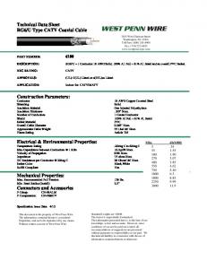
6100. DESCRIPTION: RG6/U – 1 Conductor 18 AWG Solid, 100% Al. Foil + 61%
Al. Braid and an overall PVC Jacket. ... Temperature Rating ... conditions of use
are beyond our control, all ... This document is the property of West Penn Wire.
DOVER DE109 is the excellent product in IC bonding as one kind of the single-epoxy adhesive. It's specially used in the
TECHNICAL DATA SHEET. Packaging. Code. 4 x 3.8 L (4 ... EP40 is designed to clean up the toughest stains and is safe on
DE103 is the excellent product in IC bonding as one kind of the single-epoxy adhesive. It's specially used in the encaps
Jan 26, 2012 - Putty (WR-2) fully cures in 16 hours, at which time it can be machined, drilled, or painted. FOR BRIDGING
Newage Stamford industrial generators meet the ... supplies power via the
Automatic Voltage Regulator ... ample space for the customers' wiring and gland.
The series SR and SRM safety cable pull switching devices developed and
manufactured by BERNSTEIN AG are designed and approved in accordance
with ...
Valvoline Premium Conventional multigrade motor oils are formulated with ...
Valvoline Durablend, Valvoline SynPower motor oils(see owner's manual).
Aviation Headsets and Headphones ... The Telex Airman 750 is a lightweight,
general aviation headset complete with ... Airman 750/760 Wiring Diagrams.
Viscosity @ 25°C, CPS. Pot life @ 25°C, Days. Shelf life @ 5°C, Months ... fifteen minutes; get medical attention. Wa
allow for heat up period. Typical Properties of Cured Material. Cured for 30 minutes @150â. Physical Properties: Densi
... time at different temperatures. These times are defined from the moment the adhesive reaches cure temperature. In pr
SAC305 is a lead-free alloy that contains 96.5 % tin, 3% silver, and 0.5% ... When
used in wave soldering, AIM's SAC305 bar solder offers far superior fluidity.
The L200 is a monolithic integrated circuit for volt- age and current
programmable regulation. It is available in Pentawatt® package or 4-lead TO-3
metal case.
L200
®
ADJUSTABLE VOLTAGE AND CURRENT REGULATOR ADJUSTABLE OUTPUT CURRENT UP TO 2 A (GUARANTEED UP TO Tj = 150 °C) ADJUSTABLE OUTPUT VOLTAGE DOWN TO 2.85 V INPUT OVERVOLTAGE PROTECTION (UP TO 60 V, 10 ms) SHORT CIRCUIT PROTECTION OUTPUT TRANSISTOR S.O.A. PROTECTION THERMAL OVERLOAD PROTECTION LOW BIAS CURRENT ON REGULATION PIN LOW STANDBY CURRENT DRAIN
DESCRIPTION The L200 is a monolithic integrated circuit for voltage and current programmable regulation. It is available in Pentawatt® package or 4-lead TO-3 metal case. Current limiting, power limiting, thermal shutdown and input overvoltage protection (up to
Pentawatt®
TO-3 (4 lead)
60 V) make the L200 virtually blow-out proof. The L200 can be used to replace fixed voltage regulators when high output voltage precision is required and eliminates the need to stock a range of fixed voltage regulators.
ABSOLUTE MAXIMUM RATINGS Symbol
Value
Unit
Vi
DC Input Voltage
Parameter
40
V
Vi
Peak Input Voltage (10 ms)
60
V
∆Vi-o
Dropout Voltage
32
V
Io
Output Current
internally limited
Ptot
Power Dissipation
internally limited
Tstg
Storage Temperature
Top
Operating Junction Temperature for L200C for L200
-55 to 150
°C
-25 to 150
°C
-55 to 150
°C
THERMAL DATA TO-3
Pentawatt®
Rth j-case
Thermal Resistance Junction-case
Max
4 °C/W
3 °C/W
Rth j-amb
Thermal Resistance Junction-ambient
Max
35 °C/W
50 °C/W
January 2000
1/12
L200 CONNECTION DIAGRAMS AND ORDER CODES (top views)
Type
Pentawatt®
L200 L200 C
TO-3 L200 T
L200 CH L200 CV
L200 CT
BLOCK DIAGRAM
APPLICATION CIRCUITS Figure 1. Programmable Voltage Regulator with Current Limiting
2/12
Figure 2. Programmable Current Regulator.
L200 SCHEMATIC DIAGRAM
ELECTRICAL CHARACTERISTICS (Tamb = 25 °C, unless otherwise specified) Symbol
Parameter
Test Conditions
Min.
Typ.
Max.
Unit
4.2
9.2
mA
VOLTAGE REGULATION LOOP Id
Quiescent drain Current (pin 3)
Vi = 20 V
eN
Output Noise Voltage
Vo = Vref B = 1 MHz
Vo ∆ Vo Vo ∆ Vi
µV
80
Output Voltage Range
Io = 10 mA
Voltage Load Regulation (note 1)
∆Io = 2 A ∆Io = 1.5 A
Line Regulation
V0 = 5 V Vi = 8 to 18 V
48
60
dB
V0 = 5 V Io = 500 mA ∆Vi = 10 Vpp f = 100 Hz (note 2)
48
60
dB
∆ Vo SVR
Io = 10 mA
Supply Voltage Rejection
2.85 0.15 0.1
∆Vi-o
Droupout Voltage between Pins 1 and 5
Io = 1.5 A
∆V0 ≤ 2%
Vref
Reference Voltage (pin 4)
Vi = 20 V
Io = 10 mA
2.64
36
V
1 0.9
% %
2
2.5
V
2.77
2.86
V
3/12
L200 ELECTRICAL CHARACTERISTICS (continued) Symbol
Parameter
∆Vref
Average Temperature Coefficient of Reference Voltage
I4 ∆ I4
Test Conditions Vi = 20 V
Min.
Io = 10mA for Tj = - 25 to 125 °C for Tj = 125 to 150 °C
3
Average Temperature Coefficient (pin 4)
Zo
Output Impedance
Vi = 10 V Io = 0.5 A
Vo = Vref f = 100 Hz
Vi = 10 V I5 = 100 mA
Vo = Vref
Max.
-0.25 -1.5
Bias Current and Pin 4
∆ T • I4
Typ.
Unit mV/°C mV/°C
10
µA
-0.5
%/°C
1.5
mΩ
CURRENT REGULATION LOOP VSC ∆ VSC ∆ T • VSC ∆ Io
Current Limit Sense Voltage between Pins 5 and 2 Average Temperature Coefficient of VSC
Current Load Regulation
Io
ISC
0.38
Peak Short Circuit Current
Vi = 10 V Io = 0.5 A Io = 1A Io = 1.5 A
∆Vo = 3V
Vi - V0 = 14 V (pins 2 and 5 short circuited)
0.45
0.52
0.03
%/°C
1.4 1 0.9
% % % 3.6
Note 1: A load step of 2 A can be applied provited that input-output differential voltage is lower than 20 V (see Figure 3). Note 2: The same performance can be maintained at higher output levels if a bypassing capacitor is provited between pins 2 and 4.
Figure 3. Typical Safe Operating Area Protection.
4/12
V
Figure 4. Quiescent Current vs. Supply Voltage.
A
L200 Figure 5. Quiescent Current vs. Junction Voltage.
Figure 6. Quiescent Current vs. Output Current.
Figure 7. Output Noise Voltage vs. Output Voltage.
Figure 8. Output Noise Voltage vs. Frequency.
Figure 9. Reference Voltage vs. Junction Temperature.
Figure 10. Voltage Load Regulation vs. Junction Temperature.
5/12
L200 Figure 11. Supply Voltage Rejection vs. Frequency.
Figure 12. Dropout Voltage vs. Junction Temperature.
Fi g ure 13 . Ou tpu t Imped ance vs. Frequency.
Figure 14. Output Impedance vs. Output Current.
Figure 15. Voltage Transient Reponse.
Figure 16. Load Transient Reponse.
6/12
L200 Figure 17. Load Transient Reponse
Figure 18. Current Limit Sense Voltage vs. Junction Temperature.
APPLICATIONS CIRCUITS Figure 19. - Programmable Voltage Regulator
Figure 20. - P.C. Board and Components Layout of Figure 19.
Figure 21. - High Current Voltage Regulator with Short Circuit Protection.
Figure 22. - Digitally Selected Regulator with Inhibit.
7/12
L200 Figure 23. Programmable Voltage and Current Regulator.
Note: Connecting point A to a negative voltage (for example - 3V/10 mA) it is possible to extend the output voltage range down to 0 V and obtain the current limiting down to this level (output short-circuit condition).
Figure 24. High Current Regulator with NPN Pass Transistor.
8/12
Figure 25. High Current Tracking Regualtor.
L200 Figure 26. High Input and Output Voltage.
Figure 27. Constant Current Battery Charger.
The resistors R1 and R2 determine the final charging voltage and R SC the initial charging current. D1 prevents discharge of the battery throught the regulator. The resistor RL limits the reverse currents through ther regulator (which should be 100 mA max) when the battery is accidentally reverse connected. If RL is in series with a bulb of 12 V/50 mA rating this will indicate incorrect connection.
Figure 28. 30 W Motor Speed Control.
Figure 29. Loww Turn on.
Figure 30. Light Controller.
9/12
L200
DIM. A C D D1 E E1 F F1 G G1 H2 H3 L L1 L2 L3 L4 L5 L6 L7 L9 M M1 V4