Abstract-In this paper we show a possible perspective for networks of distributed sensors based on organic field effect transistors assembled on a yarn.
Proceedings of the 3rd IEEE-EMBS International Summer School and Symposium on Medical Devices and Biosensors MIT, Boston, USA, Sept.4-6, 2006
The textile transistor: a perspective for distributed, wearable networks of sensor devices Maurizio Maccioni, Emanuele Orgiu, Piero Cosseddu, Simone Locci and Annalisa Bonfiglio
Organic materials, based on conjugated organic small molecules and polymers, offer the opportunity to produce devices on large-area, low-cost, plastic planar substrates [3] These materials are becoming of great appeal also in the field of e-textiles [4] as they show an interesting combination of electronic and mechanical properties that can be favorably exploited in smart textiles. Nowadays to our knowledge, only few steps towards new architectural possibilities have been made: one example of non planar devices [5] and one of textile based devices [6], both giving a chance to the realization of circuit topologies implementable with textile techniques. . A number of applications, as for instance smart textiles systems for biomedical monitoring functions [7], or new man-machine interfaces [8], could greatly benefit from this possibility.
Abstract-In this paper we show a possible perspective for networks of distributed sensors based on organic field effect transistors assembled on a yarn. The electronic yarn will allow to obtain matrices of sensors assembled by textile technology and will ensure to obtain for wearable devices the necessary properties of drapability and conformity to the body.
I. INTRODUCTION T he e-textile era is shortly becoming a reality. l Currently, e-textile products are being developed in view of their application in the field of biomedical monitoring [1], sports and emergency/high risk workers [2], but it is already predictable that soon e-textiles will become a reality also in the everyday life. For fabric becoming a feasible platform for electronics, much work remains to be done. In particular, the crucial point is that E-textiles must have the revolutionary ability to sense, act, store, emit, and move while leveraging an existing low-cost textile manufacturing infrastructure and to do this, it is necessary to pass from the simple concept of wearable electronics (electronic equipment that thanks to its size, packaging, or function can be applied or linked to a garment) to the more challenging idea of electronic yarns and textile circuits. In this paper, we report on cylindrical organic fieldeffect transistors that have been obtained starting from a metallic fiber used in textile processes. The metal core of the yarn, covered with a thin polyimide layer, is the gate of the structure; a top contact device has been obtained by depositing on it a layer of organic semiconductor followed by the deposition of source and drain top contacts. These can be made by metals or conductive polymers, and deposited by evaporation or soft lithography. This last technique seems to be particularly useful for producing multiple devices along the fibers and because it allows to use materials with mechanical properties that do not compromise the flexibility of the yarn. Thanks to the flexibility of the structure and the low cost of technologies, this device is a meaningful step towards innovative applications of textile electronics. All authors are with the University of Cagliari Department of
II. EXPERIMENTAL In this paper, we present an example of organic field effect transistor characterized by a size and geometry fully compatible with textile processes. The device has been obtained starting from a cylindrical metal fiber with a diameter of 45 pim, covered by a uniform layer of polyimide of about 1 pm (Elektrisola). As a result, this yarn is very flexible and can be employed, twisted to a cotton fiber, in textile processes.
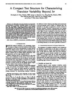
Fig. 1, Structure of the cylindrical OFET.
We have obtained a cylindrical top-contact OFET (general structure shown in fig. 1), by evaporating Pentacene (Sigma Aldrich) on the structure. After this step, source and drain contacts have been realized in two different ways: either by evaporating gold electrodes directly on pentacene by interposing a thin crossing wire as a shadow mask during the evaporation procedure (in this way, a channel length with almost the same size of the wire diameter is obtained, but a good control on
Electric and Electronic Engineering, Piazza d'Armi 09123 Cagliari, Italy and with INFM-S3 "nanoStructures and bioSystems at Surfaces", Modena, Italy The work was supported by EU Commission, under the ISTIntegrated Project PROETEX, contract n. 26987
0-7803-9787-8/06/$20.00 ©2006 IEEE
5
dimensions is not possible) or, by employing a soft lithographic process for transferring a thin layer of the conductive polymer PEDOT:PSS on the pentacene surface. This method has several advantages: it allows to exploit the favorable mechanical properties of conductive polymers as contacts; it allows to have an optimal control of geometries because the relieves of the stamp used for soft lithography are obtained with a high resolution technique as already demonstrated for planar devices [9] (from photolithography to a number of high resolution techniques [10]); it allows (by rotating the yarn on the stamp surface) to deposit contacts on the whole surface of the yam (while with evaporation only the side exposed toward the crucible is uniformly covered); it allows to easily make a whole set of contacts along the wire length at the same time.
VdsM
a b Fig. 3, Id-Vd curves of cylindrical OFET structures, having source and drain contacts made by gold (on the left) and by PEDT:PSS contacts (on the right)
In addition, we estimated the series resistance effect according to the concept proposed by Horowitz [11], but fitting the whole I-V curves in order to have a reliable value of all free parameters of the model (threshold voltage, mobility, Series Resistance). We found a difference in devices made with gold contacts with respect to those obtained by soft lithography assembling of PEDT:PSS contacts.
PDOMS gate
V drain
V Source
Device
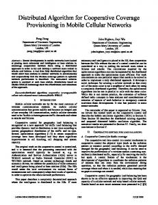
TABLE I COMPARATIVE PERFORMANCE OF DEVICES Ion/loff Vt (V) 4t(cm2/Vs) Rs (MOhm)
Fig. 2, Measure setup for the device made by soft-lithographic stamping PEDT:PSS contacts.
Gold contacts device
7x10
-17.3
0.04
32
A complete electrical characterization has been made, in air, by means of a HP 4155 Semiconductor Parameter Analyzer (for ID-VD and ID-VG curves) and by means of Agilent 4284A Precision LCR Meter 2OHz-IMHz (for C-V curves), provided with gold tips. In devices with gold contacts, the gold tips have been simply pressed against source and drain of the transistor wire. In devices with PEDT:PSS contacts (fig. 2), the measurements have been made by sandwiching the wire between a cover slide where two gold electrodes had been previously deposited and a PDMS stamp reproducing source and drain covered with a thin layer of PEDT:PSS (Baytron P CPP 105D).
PEDT:PSS contacts device
3x10
-9.6
0.06
14
3
3
In table I, the main parameters are shown for a couple of representative devices. As can be observed, the device with Gold contacts shows a lower value of mobility, together with a higher value of Series Resistance. In addition, also the threshold voltage is more negative. Therefore, it seems that, despite the better value of the Ion/loff ratio (estimated on curves with the same (VGVT) value), the trend for the main electronic parameters is more favourable in devices with PEDT:PSS contacts. Obviously this issue is of great importance, especially in view of future applications in "textile circuits", because the fabrication process of multiple PEDT:PSS contacts on yarns is potentially easier and can be made in parallel on several yarns. In addition, PEDT:PSS is a polymer with mechanical properties similar to those of the organic semiconductor. Therefore, both semiconductor and contact layers do not compromise the flexibility of the yarn which is uniquely determined by the core of the yarn. It is worth noting that the derived Mobility values in cylindrical devices are comparable if not better than those recorded for polycristalline Pentacene on planar devices. In order to better understand the reason for this behaviour, we performed AFM investigations on the channel area of the wire (fig. 4).
III. RESULTS In fig. 3 the ID-VD curves of a device with gold source and drain (3a) and PEDT:PSS contacts (3b) are shown. It is worth to note that establishing a reliable electrical contact with source and drain was particularly difficult due to the very low dimensions and also to the non-
planar surface of the wire. Interestingly enough, despite the above mentioned problems and the very low value of the W/L ratio (estimated as 1.2), the ON current and, most of all, the Ion/loff ratio is reasonably high (around 104), fully comparable with those of planar devices. In order to derive a reliable estimation of the electronic parameters, we fitted the I-V curves with an electronic model that takes account of the cylindrical geometry of the devices [10].
6
IV. CONCLUSIONS
In conclusion, we have obtained a cylindrical organic thin film transistor that, due to its form factor and the employed materials, is fully compatible with a textile process (weaving and knitting equipment). This transistor has shown very interesting performances, with typical values of the electronic parameters (mobility, threshold, Ion/loff ratio) very similar to those of planar devices. This result is very promising in view of innovative applications in the field of smart textiles. In particular, the realization of distributed transistors and sensors in a textile network is the natural, most promising perspective for a variety of applications.
Fig. 4, The device channel observed by optical microscopy and by AFM.
The morphology of the pentacene layer is pretty regular, with the typical granular aspect that is observed also when Pentacene is deposited on planar insulating layers. In comparison with Pentacene depositions made with the same evaporation parameters (rate, distance on between crucible and sample) polyethileneterephtalate substrates, that we typically use as insulating films of planar OFETs [8], the mean dimension of the domains is significantly higher. Typical grain dimensions around 150 nm have been found for pentacene grown on polyethileneterephtalate, while, in this case, we obtained grain dimensions in the range of 200-250 nm. Considering a model where the mobility is limited by traps localized at grain boundaries, this should coherently result in a higher value of mobility. This is confirmed by the electrical measurements, where a typical value of some 3-6 10-2 Vcm/s2 has been recorded for cylindrical transistor (while in planar devices the typical value is lower than 10-2) showing that polyimide, as previously reported in literature for planar devices [12], forms a good insulator/organic semiconductor interface. Therefore, the good performance obtained with these cylindrical devices paves the way towards the realization of simple circuits obtained by crossing the transistoryarn with conductive yarns that contact source and drain contacts distributed along the yarn. In this way, it is possible to obtain a textile matrix that is particularly interesting for future developments in distributed sensor systems made on a textile platform. For instance, deformation sensors arranged according to a matrix as suggested in [7], but taking advantage from the textile form of the transistors, could be of great benefit for the realization of a robotic "skin".
ACKNOWLEDGMENT
European Commission is gratefully acknowledged for funding the project under the Programme IST-IP, VI FP Project n. 26987, PROETEX. REFERENCES
[1].
[2]. ht/wpo
[3] IEEE Proceedings, Special Issue on Flexible Electronics Technology, Part I: Systems and Applications [4] F. Carpi and D. De Rossi, IEEE Transactions on Information Technology in Biomedicine 9, 295 (2005). [5] J.B. Lee, V. Subramanian, IEEE Trans. on Electron Devices, 52 (2), 269-275 (2005) [6] A. Bonfiglio, D. De Rossi, T. Kirstein, I. Locher, F. Mameli, R. Paradiso, G. Vozzi, "Organic field effect transistors for textile applications", IEEE Transaction on Information Technology in Biomedicine, 9, 319-324 (2005) [7] T. Someya, T. Sekitani, S. Iba, Y. Kato, H. Kawaguchi, and T. Sakurai, "A large-area, flexible pressure sensor matrix with organic field-effect transistors for artificial skin applications," Proc. Nat. Academy of Sciences USA, vol. 101, no. 27, pp. 9966-9970, Jul. 6, 2004. [8] P. Cosseddu, A. Bonfiglio, Appl. Phys. Lett. 88, 23506 (2006) [9] Y. Xia and G. M. Whitesides, Angew. Chem., Int. Ed. 37, 550 (1998). [10] S. Locci, M. Maccioni, E. Orgiu, A. Bonfiglio, manuscript in preparation [1 I].G. Horowitz, P. Lang, M. Mottaghi, and H. Aubin, Adv. Funct. Mater. 14, 1069 (2004). [12] K N Narayanan Unni, S. Dabos-Seignom and J-M Nunzi, Appl. Phys. Lett. 38, 1148 (2005).
7