A Field-Effect Transistor with a Negative. Differential Resistance. Abstract-We report the effect of negative differential resistance. (NDR) in the drain circuit of a ...
IEEE ELECTRON DEVICE LETTERS, VOL. EDL-5, NO. 2 , FEBRUARY 1984
A Field-Effect Transistor with a Negative Differential Resistance Abstract-We reporttheeffectofnegativedifferential resistance (NDR) in the drain circuit of a new type of selectively-doped AlGaAs/ GaAs heterojunction transistor. The keynew element of our structure is the presence of a subsidiary GaAs conducting layer, separated from the FET channel by an AlGaAs gradedbarrier. In this work the subsidiarylayerisrealized by the conductingsubstrate. The NDR effect arises due to the heating of channel electrons by the source-todrain field, and the subsequent charge injection over the barrier. This effect is strongly influenced by the gate and substrate voltages. In a floating-substratearrangementthe current-voltage characteristics exhibit memory effects associatedwith retention of injected charge in the substrate. In this mode, the NDR is seen only at low temperatures 77 K reaching values as with the peak-to-valley ratios in current at high as 30. On the other hand, whenthe substrate is biased positively, the NDR results from a peculiar effect of dynamical channel depletion by the injected space charge which drifts on the downhill slope of the gradedbarrier.Inthiscase, the NDR is observedeven at room temperature.
I
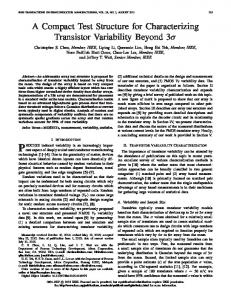
GRAOED B A R R IAE?SR,
UNODPEO
GaAs SUBSTRATE ND=1D18cm-a
I - - l - - - Y EF
V,,b
Fig. 1. NERFET structureandenergybanddiagram.Regions,where the electron gas is degenerateareindicatedinblackontheband diagram. Dimensions: 1 = 1450 A, d = 190 A. The content of aluminum in the barrier is graded from x = 0.1 1 to x = 0.34.
N ARECENT PAPER [ l ] we proposeda new device concept based onhot-electrontransferbetweentwoconducting layers ina AlGaAs/GaAs heterostructure. One of theselayers is an FET channel, and it is separated from the secondlayerby a graded A1,Gal -,As potentialbarrier. Application of a source-to-drainfield causes heating of channel electrons and an exponentially enhanced charge injection into the second layer. This phenomenon was expected to produce astrong negative differential resistance (NDR) in the drain circuit.Theproposed device received thenameNERFET, which stands for negative resistance field-effect transistor. Fig.1 shows the device structureanditsband diagram. It has been grown bymolecular-beamepitaxy (MBE) on Si-doped (10' ~ m - ~GaAs ) substrate, whictl plays the role of the second conductinglayer. We used a {loo} substrate orientationanda 64OoC growthtemperaturewith arsenicrich growthconditionsand conversionof the arsenic beam from As4 toAs2.Thegrowthsequencecommencedwitha 1-pm homoepitaxial layer of Si-doped (-lola ~ m - GaAs. ~ ) The content of aluminum in theundoped barrier layer of thickness I = 1450 A was graded from x = 0.1 1 to x = 0.34 by progressively increasing thealuminummolecular-beam cell temperatureduringgrowth of thelayer.Theupper GaAs conducting channel layer of thickness d = 190 was undoped. The A1.34G.8.66AS layerwhich provided theconduction
electronstothechannelcontained -2 X 1018cm-3 silicon atoms, was 390 .A thick, and was separated from the channel by an 80-A-thick undoped A1,34Ga,66 As spacer layer. For NERFET operation, itis essential that source and drain contacts to the channel were insulated from the second conducting layer, We used a Au/Ge-Ag-Au alloy which is known to give shallow (-2000 A) andabrupt ohmic contacts. We sought to have the bottom edge of contact penetration stop near the top of the graded barrier. To this end we used a thick (1400-A? silicon-doped) GaAs cap layer(making thetotal thickness of thestructure above the gradedbarrier about 2iOO A), and experimented with different alloying cycles and temperatures. Best results were obtained by alloying at 42OoC for 20 s. Fig. 2 shows the resultant current-voltage ( I s U ~ V ~ U B )curves in thesubstratescircuit (source and drain grounded)at 300 K(Fig. (2(a)) and 77 K (Fig.2(b)).These are typical rectifying characterisitcs of a one-sidedtriangular barrier of approximateheight 0.4 eV [ 2 ] . We observed no ohmic leakage down to I ~ U B 10-l' A. Devices were isolated from one another by selectively removing the conducting material between individual transistors and covering theresultant mesa patternby silicon nitride, Active device area was cutintothenitridebyaCF4/02 plasma etch. Gates were deposited after a self-aligned chemical etch through the cap layer. The gate was notched a little into the AlGaAs layer to produce a slight channel depletion and to Manuscript received November 10,1983;revised December 14,1983. ensure concentration of thesource-to-drain field in the norThe authors are withBell Laboratories, Murray Hill, NJ 07974. mally-on device. The gate (notch) length was 1 pm, while the 1 This paper contains an extensive list of references to the work of total separation between source and drain was 4 pm; we used the University of Illinoisgroupwhichpioneeredthestudyofrealspace hot-electron transfer effects. 250-pm-wide gates. ~
a
0193-8576/84/0200-0057$01.00 0 1984 IEEE
-
58
IEEE ELECTRON DEVICE LETTERS, VOL. EDL-5,NO. 2 , FEBRUARY 1 9 8 4
(b) Fig. 2. Current-voltagecharacteristicsin thesubstratecircuit.Source of alloyed contacts is 3 X and drain are grounded; the total area 10-5 cm2. (a) T = 300 K; (b) T = 7 7 K.
As discussed in [ l ] , The NERFET can exhibit NDR in two distinct configurations, depending on a circuit connection of thesubstrateterminal.Inthefloating-substratearrangement Fig. 3. Current-voltagecharacteristicsinthedraincircuit:floatingthehot-electroninjectioninduces charge inthesubstrate substrate configuration; T = 77 K. (a) I S U B= 1 PA; VG = -0.2,0, andthusshiftsthethresholdforconductioninthemain 0.2,0.4 V; (b) I S U B= 100 MA;VG = -0.2, 0,0.2, 0.4 V; (c) I S U B = 0.5 PA; floating gate. channel.This process is limitedbythermionicinjection of cold electronsfromthesubstrate whose potential is raised by the injected charge. For a barrier height $ = 0.4 eV, we Fig. 3(c) displayssuch curves withthepeak-to-valleyratio can expect a pronounced NDR in this mode only at low tem- in current reaching about 30. These characteristics were taken peratures.Fig.3(a)showsthe observed curre.nt-voltage (Io- with the substrate current, I s u = ~ 500 nA, being four orders V,) characteristicsinthe drain circuit. These characteristics of magnitude lower than the drain current. were taken in a quasi-floating configuration in which the Biased-suhtrate characteristics of the NERFET are shown substrate was positively biased througha large resistance, in Fig. 4 . We see a strong dependence of NDR on the substrate drawing a small constant current IsUB (four orders of magni- voltage V s u ~ .It should be noted that the NDR portion of tude lower than that in the drain circuit). The four curves in these curves represents an average over high-frequency oscillaFig.3(a) correspondtothe gate voltage V , varying from tions, and its shape can be affected by parasitic impedances -0.2 to 4-0.4 V. We see that higher VG suppresses the NDR introducedby an experimentalsetup. The rising portion of in accordancewiththetheoreticalpredictions [ l ] . We also I-V curves at high V, corresponds to the onset of the thermsee apronounced hysteresis inthe’ 1 o - V ~ characteristics, ionicemission of coldelectronsfromthesubstrateintothe which indicatesamemoryeffect. Thismeans that electrons drain. It is shifted to the right by increasing VSUB, The obtransferredintothe second conducting layerremain there served strong effect of VsUB on the depth of NDR is, in our whenthe drain voltage is reduced. The transferredelectrons view, related to the dynamical charge storage effect discussed are free to move within the heavily doped second conducting in [ l ] . Hot electrons emitted over the top of the barrier drift layer, Le., they are not localized on any traps. In the absence downhill with a saturated velocity u,, and constitute a space of I S U B :theretention time is determinedbythe reverse charge of volume density p = J/v, E h / l , where J is the subthermionic emission of “cold”electronsfromthesubstrate, stratecurrentdensity and Ao thesurfacedensity of charge which at low temperatures is a slow process. Introduction of stored in transit on the barrier of thickness 1. For an efficient a substrate leakage reduces the memory effect and at higher depletion of thechannelonemust have Ao I/vs, where I ~ U the B latter is no longerobserved(Fig. 3(b)). Character- I 2to3A/cm is thepeakchannelcurrentperunit gate istics obtained at 4.2 K were quite similar to those at 77 K, width, cf., Fig. 4. Assuming that the saturated velocitiesare which is another evidence that trapping effects in the AlGaAs -IO7 cm/s both in the channel and on thebarrier, we find barrier region are not important. Au % 2 X 1 O I 2 e/cm2.. This correspondstoa space-charge When boththesubstrateandthe gateare floating,the potential A$ = p12/2e 2 V.Inorderto overcomethis device shows symmetriccharacteristics on a curve tracer. additional barrier, the substrate bias V s u ~must exceed
-
KASTALSKY et al.: FIELD-EFFECT TRANSISTOR WITH A NEGATIVE RESISTANCE
59
Fig. 4. Current-voltage characteristics in the drain circuit: biased-substrate configuration; T = 77 K ; VG = 0.
A$. Thus fortheindicatedcurrent
densities inthe biasedsubstrate configuration the NDR is obtained only when VsuB 2 2 V, see Fig. 4. We remarkthatdynamical chargestorage dueto spacechargeJimitedcurrent is an importantfactor in mostunipolar devices. In these devices theinjected chargescreens the appliedfield and limits the efficiencyof injection (for a detailed discussion of charge injection in field-effect and analog transistors see [3], [4] >. Unlike in anyother device with space-charge-limited current,inNERFET this current Fig. 5 . NERFET at room temperature: biased-substrate configuration; VSLB = 2.4 V; VG = 0.6 V (T = 300 K). flows perpendicular to the main conducting channel andresults in the desired effect of channel depletion and NDR. It is interesting to note that the decrease in ID in the NDR region where A is the channel thickness and Te the electron temperadoes not necessarily imply a simultaneous increase in I S U B . ture, we findthatthedensity of charge in the high-field Moreover, the first appearance of the NDR is, in fact, accom- domain decays exponentially from the beginning of the panied by a small drop in the substrate current.We believe this domain and towardthe drain with a characteristiclength effect is associated with the formation of a narrow high-field h = A ~ , ( k T ~ / 2 . i r r n )exp - ~ ~(e$/kTe). ~ The effective extent domaininthechannelinthe vicinity of the drain. Concenof the hot filament is, thus determined by the electron temtration of theelectron field enhances hot-electron injection. perature, and at high T , itmay be narrower thanthehighOntheotherhand,concentration of thesubstratecurrent field domain. in anarrowstrip(“hotfilament”,extending over the 250 Thedynamical chargestorage effect can be expectedto pm of gate width) results in a higher density of the dynami- have onlyaweakdependenceonthelatticetemperature cally stored charge and further depletion of the channel. In (mainly through the dependence Te(T) inthe high-field this process, the increasing density J of the substrate current domain). Fig. 5 shows the observed characteristics at T = 300 does not necessarily imply higher ISUB . K inthebiased-substrateconfiguration.Dependence of the Dimensions of the hot filament can be estimated from the room temperature characteristics on VSUB and V , was continuityequationforthechannelcurrent I(x) per unit qualitatively similar tothatat 77 K. Inparticular,thesubgate width, dI/dx = J ? where x is the direction of the channel. strate works as abackgate,Le., positive VSUB enhances the Taking I = uuJ in the high-field domain and density of charge in the channel and therefore the peakvalue
J=? A
.J”.-e$/kTe
2rrm
of the drain current. We never observed an NDR effect at 300 K in the floatingsubstrate configuration. This underscores the difference in the physicalprinciples involved in the operation of NERFET in
VOL. LETTERS, ELECTRON DEVICE IEEE
EDL-5, NO. 2 , FEBRUARY 1984
these two circuit configurations: static versus dynamic charge storage. We believe thatsubstrate-biased NERFE’I may become useful as an efficientgenerator of microwaves in the millimeter-wave region, controllable by the gate and substrate voltages. Of particular importance is the complete absence of memory effects in the dynamic mechanism. In a recent work [5] we observed the microwavegeneration in NERFETin the gigahertzrange. It is experimentally demonstrated in [5] that the NDR and the associatedinstabilitiesare not related to spurious oscillations often observed in transistors with poor isolation, Estimates show [6] that the intrinsic speed of operation in NERFET is limitedbythe energy relaxationtime andthetime of flightof electrons over the graded barrier, both of these delays being of order several picoseconds.
A. Kastalsky and S. Luryi, “Novel real-space hot-electron transfer devices,” I€€€ Electron Device Letr.. vol.EDL-4, no. 9 , pp. 334-336,1983. C. L. AIIyn, A . C. Gossard, and W. Wiegmann, “New rectifying semiconductor structure by molecular beam epitaxy,” Appl. Phys. Lett., vol.36.pp.373-376,1980. R . F. Kazarinov and S. Luryi, “Majority carrier transistor based on voltage-controlled thermionic emission,” A p p l . Phys., vol. A 28, pp. 151-160, 1982. S . Luryi and R. F. Kazarinov, “On thetheory of thethermionic emission transistor; TET as an element of logic circuits.” SolidState Electron., vol. 25, pp. 933-942, 1982. R. Kiehl, A. Kastalsky, S . Luryi, A . C. Gossard, and R . Hendel, “Microwave generation in NERFET,” to be published. S. Luryi, A. Kastalsky, A. C. Gossard, and R. Hendel,“Charge injection transistor based on real-space hot-electron transfer,”to be published.
60
REFERENCES