PHYSICAL REVIEW B, VOLUME 63, 104425
Spin-polarized electron transport in ferromagnetÕsemiconductor hybrid structures induced by photon excitation A. Hirohata, Y. B. Xu, C. M. Guertler, and J. A. C. Bland* Cavendish Laboratory, University of Cambridge, Madingley Road, Cambridge CB3 0HE, England
S. N. Holmes Cambridge Research Laboratory, Toshiba Research Europe Limited, 260 Cambridge Science Park, Milton Road, Cambridge CB4 0WE, England 共Received 24 October 2000; published 20 February 2001兲 Circularly polarized light was used to excite electrons with a spin polarization perpendicular to the film plane in 3 nm Au/5 nm Ni80Fe20 /GaAs(100) structures with doping density in the range 1023 to 1025 m⫺3. At negative bias a helicity-dependent photocurrent dependent upon the magnetization configuration of the film and the Schottky barrier height was detected. The helicity-dependent photocurrent polarization decreases with increasing doping density and has the same variation with photon energy as found for the polarization of photoexcited electrons in GaAs. The results provide unambiguous evidence of spin-dependent electron transport through the NiFe/GaAs interface and show that the Schottky barrier height controls the spin-dependent electron current passing from the semiconductor to the ferromagnet. DOI: 10.1103/PhysRevB.63.104425
PACS number共s兲: 85.70.Kh, 73.30.⫹y, 73.40.Gk
Since the possibilities for developing a spin-dependent field effect transistor 共spin FET兲 were first raised by Datta and Das,1 a great number of studies2–5 on device structures based on ferromagnet 共FM兲/semiconductor 共SC兲 hybrid systems have been carried out. A spin FET for example offers the prospect of fast operation and miniaturization.2 As the device operation would depend on the injection of a spindependent current into the SC, it is important to clarify the FM/SC interface transport process. The possibility of passing a spin-dependent current through thin film tunnel junctions of both Co/Al2O3 /GaAs and Co/-MnAl/AlAs/GaAs has been discussed by Prins et al.6 For the former structure, a spin-dependent tunneling current was reported. In the latter structure, however, only magneto-optical effects were seen. A great many studies of spin-dependent tunneling through metal/oxide insulator/ semiconductor 共MOS兲 junctions have been reported.7 Some recent experiments suggest8 that such systems may provide possibilities for spin-polarized scanning tunneling microscopy 共SP-STM兲.9,10 However, due to the presence of the oxide layer, the mechanism of the spin-dependent tunneling through the MOS junction is extremely complicated. For the direct FM/SC interface, a Schottky barrier arises which also gives rise to tunneling under appropriate bias conditions. However, it is still not clear whether spin-dependent tunneling at the direct FM/SC interface through the Schottky barrier occurs and is detectable. Evidence of spin-dependent current effects associated with photoexcited electron transport at Schottky diode interfaces based on NiFe/GaAs has been demonstrated recently in forward bias.11 However, only a small effect, comparable with the estimated magnitude of magneto-optical effects, was observed in reverse bias and therefore no firm conclusions concerning the possibility of spin tunneling could be drawn. In such experiments, the advantage of photoexcitation is that the electron polarization in the SC can be controlled via the light polarization. 0163-1829/2001/63共10兲/104425共4兲/$15.00
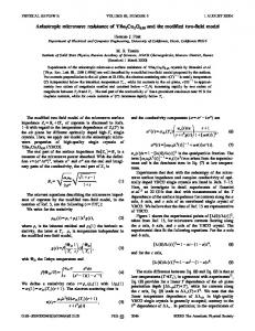
In this study, in order to clarify the Schottky barrier height dependence of possible spin-polarized transport effects, we fabricated 5 nm thick ferromagnetic layers (Ni80Fe20) directly onto GaAs 共100兲 substrates in an ultrahigh vacuum 共UHV兲 chamber. Conventional I-V measurements were performed both with and without photon excitation. A circularly polarized laser beam was used together with an external magnetic field to investigate the spindependence of the photocurrent at the NiFe/GaAs interface at room temperature. Since permalloy has a large polarization difference at its Fermi level12 and a small magneto-optical background 关due to magnetic circular dichroism 共MCD兲兴, it is an appropriate choice for the spin-dependent transport experiment. Since the epitaxial growth of FM transition metals on GaAs substrates has been well investigated,4,13 GaAs substrates were chosen for the present study. Moreover, we varied both the photon energy and the doping density in order to probe for spin transport across the Schottky barrier since stronger effects might be expected as the photon energy approaches the GaAs band gap, while varying the doping density allows the Schottky barrier height and the depletion layer width to be modified. This study was carried out using a conventional photon excitation setup with front illumination at room temperature 共see Fig. 1兲.6,11 Conventional I-V measurements were carried out to investigate the Schottky characteristics of the samples. Laser light 共⫽514.5, 632.8, and 780.0 nm兲 perpendicular to the sample surface was used and the bias dependence of the current through the NiFe/GaAs interface (⫺2.5⬍V⬍1.5 V) was measured both with and without optical excitation. The polarization of the beam was then modulated from right circular to left circular polarization using a photoelastic modulator 共PEM兲 with 100% circular polarization at a frequency of 50 kHz. For the polarized illumination mode, the bias dependence of the ac helicity-dependent photocurrent I
63 104425-1
©2001 The American Physical Society
HIROHATA, XU, GUERTLER, BLAND, AND HOLMES
PHYSICAL REVIEW B 63 104425
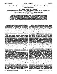
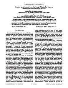
FIG. 1. Schematic configuration of the photon excitation experiment. The laser is polarized in the 45° direction. Right/left circular light is produced using a PEM. The bias dependent photocurrent is determined by I – V measurement methods combined with a lock-in technique. A schematic view of the Ni80Fe20 /GaAs hybrid structure sample (3 mm⫻3 mm) is also shown in this diagram. Two Al contacts on the surface (0.5 mm⫻0.5 mm⫻550 nm) and an Ohmic contact on the bottom are used for the measurement. The value of the variable resistance for the measurement was chosen to be approximately the same as that of the resistance between the Ni80Fe20 and the GaAs substrate 共n⫽1023, 1024 and p⫽1025 m⫺3 doped兲, typically 60, 200, and 15 ⍀, respectively. Magnetization M in the FM and photon helicity are also shown with the field application.
through the interface was probed with the same sample both in the remanent state (I 0 ) and under the application of a magnetic field (H⫽1.8 T) sufficient to saturate the magnetization along the plane normal (I n ). In the case of I 0 , the photon helicity is perpendicular to the magnetization of the FM, while the helicity is either parallel or anti-parallel to the magnetization for I n . I 0 and I n are a measure of the difference in photocurrent for right and left circular polarization for the in-plane and perpendicular magnetization configurations, respectively. We produced a sample of 3 nm Au/5 nm NiFe/GaAs 共100兲 共n⫽1023, 1024 and p⫽1025 m⫺3兲 using molecular beam epitaxy 共MBE兲 techniques in UHV. Since In contacts are known to create a weak Schottky barrier at the interface, which can act as a series resistance,11 the Ohmic contacts on the bottom of the n and p-type substrates were prepared by evaporating 100 nm thick GeAuNi and AuBe, respectively, and then annealing at 770 K for two minutes. The GaAs substrates were then cleaned for two minutes using an oxygen plasma and loaded into the UHV chamber. The NiFe films were epitaxially grown at a rate of approximately one monolayer per minute by e-beam evaporation. The substrate temperature was held at 300 K and the pressure was around 7⫻10⫺10 mbar during the growth. The deposition rate was monitored by a quartz microbalance which was calibrated using RHEED oscillations of Fe on a Ag共100兲 single crystal. After the growth, the NiFe films were covered by a Au capping layer. Two Al electrical contacts 共550 nm thick兲 were evaporated on the Au layer. A computer controlled bias volt-
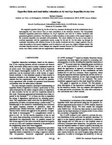
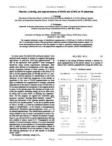
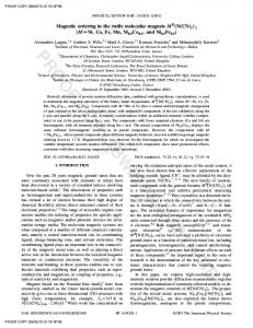
FIG. 2. 共a兲 Bias dependence of the current through the Ni80Fe20 /GaAs interface obtained without photon excitation 共I – V curve兲. Bias dependence of the helicity-dependent photocurrent without 共solid line with open circles, I 0 兲 and with the applied magnetic field 共solid line with closed circles, I n 兲 in the case of n ⫽1023 m⫺3 doped substrate 共b兲 with ⫽780.0 and 共c兲 514.5 nm. Magnetization M in the FM and photon helicity are also shown without and with the field application.
age was applied between one Al contact and the bottom Ohmic contact and the current through the other Al contact and the substrate was measured using a lock-in technique. As the polarized laser beam enters from the Au capping layer side, these structures provide a way of avoiding laser absorption at the bottom surface of the SC, as occurs under back illumination.14 Figure 2共a兲 shows the I-V curves of the Ni80Fe20 samples without photon excitation measured by the usual fourterminal method. It should be noted that every I-V curve possesses a small feature 共a兲 in forward bias around the Schottky barrier height b as observed previously.11 The ideality factor14 was calculated to be 6.69, 5.37, and 4.04 for n⫽1023, 1024, and p⫽1025 m⫺3, respectively. These values
104425-2
SPIN-POLARIZED ELECTRON TRANSPORT IN . . .
PHYSICAL REVIEW B 63 104425
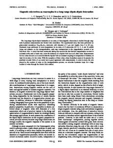
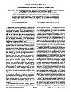
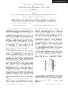
FIG. 3. Bias dependence of the asymmetry A⫽(I n ⫺I 0 )/(I n 0 ⫹I ) with n⫽1023, 1024 and p⫽1025 m⫺3 doped substrates with ⫽632.8 nm.
are comparable with those of the previously reported permalloy samples.11 The helicity-dependent photocurrent with He-Ne laser excitation (⫽780.0 nm兲 is shown in Fig. 2共b兲 with (I n ) and without (I 0 ) perpendicular saturation for the case of n ⫽1023 m⫺3. It should be noted that the helicity-dependent photocurrent values for I n and I 0 are observed to satisfy I n ⬍I 0 as previously reported, but a much larger effect is seen here due to the larger wavelength used.11 The bias dependence of the helicity-dependent photocurrent difference ⌬I (⫽I n ⫺I 0 ) of approximately 0.09 A is almost constant in the bias range of V⬍0.7 V. It should be noted that Fe/GaAs samples prepared under similar conditions to the NiFe/GaAs samples show almost no difference between I n and I 0 due to the lack of the Schottky barrier at the interface. This result confirms that the Schottky barrier is essential to achieve spin-dependent electron transport and provides a check on the experimental method. Peak A appears at V⫽0.83 V for I 0 and shifts to V⫽0.85 V for I n . The Schottky barrier height b has been reported to be 0.66–0.70 eV for Ni and Fe,11 which is approximately the same as the bias voltage for peak A. At V⬃ b , since electrons are excited in the permalloy layer by both the electrical bias and the photon energy and then propagate over the barrier,14 peak A is likely to be related to spin-dependent transport from the FM to the SC. We also show the helicity-dependent photocurrents obtained for short wavelength, corresponding to a photon energy significantly larger than the band gap in GaAs. We observe no significant difference between the helicity-dependent photocurrents obtained for the two magnetization configurations as expected. This result also provides a check on the experimental method used here. A measure of the polarization of the spin-dependent current through the NiFe/GaAs interface is provided by the asymmetry A⫽(I n ⫺I 0 )/(I n ⫹I 0 ) induced by He-Ne laser light as shown in Fig. 3 for three different values of the GaAs doping density. With n⫽1024 m⫺3, for example, almost constant asymmetry (A⬃4.5%) can be seen in the bias range of ⫺1.5⬍V⬍0.3 V, which is likely to be related to the spin-dependent photocurrent propagating from the SC to the
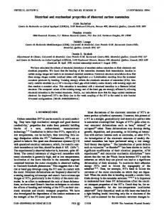
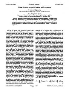
FIG. 4. Photon energy dependence of the asymmetry at V ⫽0 V with n⫽1023 and p⫽1025 m⫺3 doped substrates.
FM. For n⫽1023 m⫺3, the corresponding value is A⬃3%, while for p⫽1025 m⫺3, A⬃0. We conclude from the above results that the magnitude of the spin-dependent current in reverse bias scales with the Schottky barrier height, as is expected for spin-dependent tunneling across the barrier. This asymmetry is much larger than the estimated value 共0.2%兲 caused by MCD 共Ref. 11兲 and MCD effects can therefore be excluded. A small feature A for n⫽1023 m⫺3 (V⬃0.8 V) at the Schottky barrier height b is again seen in this figure, although the feature is small. The position of the feature is almost the same as that of peak A in Fig. 2共b兲, which indicates that the spin-dependent current from the FM to the SC is enhanced at V⬃ b . At peak A, ⌬I/I 0 is estimated to be 5%, which is much larger than that observed previously in similar samples 共due to the improved bottom contact resistance兲.11 This observation suggests that the spindependent photocurrent from the SC to the FM is suppressed by electron transport from the FM to the SC due to the reduction of b under the application of a forward bias V ⬃b . Figure 4 shows the photon energy dependence of the current asymmetry A. The magnitude of A increases with decreasing photon energy, which corresponds closely to the reported energy dependence of the photoelectron spin polarization in GaAs.9,15 The observed photon energy dependence of A therefore supports our interpretation that spin-dependent electron tunneling from the SC to the FM occurs at room temperature. In conclusion, we have observed a clear difference in the helicity-dependent photocurrent through the NiFe/GaAs interface according to the orientation of the sample magnetization with respect to the helicity at room temperature. An almost constant difference between the helicity-dependent photocurrent for perpendicular and parallel configurations is observed in reverse bias for n⫽1023 and 1024 m⫺3. This difference in photocurrent corresponds to a measure of the spindependent photocurrent tunneling from the SC to the FM. Specifically the photocurrent asymmetry approaches approximately 20% as the photon energy is lowered close to the band gap of GaAs, demonstrating that the spin transport effects are significant and excluding the possibility of experi-
104425-3
HIROHATA, XU, GUERTLER, BLAND, AND HOLMES
PHYSICAL REVIEW B 63 104425
mentally induced asymmetries. In forward bias at an applied bias voltage approximately equal to the Schottky barrier height, a minor change in the bias dependence of the helicity-dependent photocurrent was observed, suggesting the existence of polarized electron transport from the FM to the SC.
We are grateful to Professor Guangxu Cheng for assistance with the Ar laser operation. The support of EPSRC and EU 共ESPRIT兲 are acknowledged. A.H. would like to thank Toshiba Europe Research Limited, Cambridge Overseas Trust and Selwyn College 共Cambridge兲 for their financial support.
*Corresponding author. Email address:
[email protected]
Appl. Phys. Lett. 71, 3153 共1997兲. S. F. Alvarado and P. Renaud, Phys. Rev. Lett. 68, 1387 共1992兲. 10 S. N. Molotkov, Surf. Sci. 287Õ288, 1098 共1993兲; R. Laiho and H. J. Reittu, ibid. 289, 363 共1993兲. 11 A. Hirohata, Y. B. Xu, C. M. Guertler, and J. A. C. Bland, J. Appl. Phys. 85, 5804 共1999兲; 87, 4670 共2000兲. 12 S. Chikazumi, Physics of Magnetism 共Clarendon, Oxford, 1997兲, p. 172. 13 A. Schuhl, P. Galtier, O. Durand, J. R. Childress, and R. Kergoat, Appl. Phys. Lett. 65, 913 共1994兲. 14 S. M. Sze, Physics of Semiconductor Devices 共Wiley, New York, 1981兲, p. 245; E. H. Rhoderick, Metal-Semiconductor Contacts 共Clarendon, Oxford, 1978兲, p. 46. 15 D. T. Pierce, F. Meier, and P. Zu¨rcher, Phys. Lett. 51A, 465 共1975兲.
S. Datta and B. Das, Appl. Phys. Lett. 56, 665 共1990兲. 2 M. Johnson, J. Appl. Phys. 75, 6714 共1994兲. 3 A. Fert and S. F. Lee, J. Magn. Magn. Mater. 165, 115 共1997兲. 4 Y. B. Xu, E. T. M. Kernohan, D. J. Freeland, A. Ercole, M. Tselpi, and J. A. C. Bland, Phys. Rev. B 58, 890 共1998兲. 5 P. R. Hammar, B. R. Bennett, M. J. Yang, and M. Johnson, Phys. Rev. Lett. 83, 203 共1999兲. 6 M. W. J. Prins, H. van Kempen, H. van Leuken, R. A. de Groot, W. van Roy, and J. de Boeck, J. Phys.: Condens. Matter 7, 9447 共1995兲. 7 K. Nakajima, S. N. Okuno, and K. Inomata, Jpn. J. Appl. Phys., Part 2 37, L919 共1998兲. 8 K. Sueoka, K. Mukasa, and K. Hayakawa, Jpn. J. Appl. Phys., Part 1 32, 2989 共1993兲; Y. Suzuki, W. Nabhan, and K. Tanaka, 1
9
104425-4