International Journal of Advanced Research in Computer Engineering & Technology (IJARCET) ... serializer, clock and data recovery circuits and deserializer.
International Journal of Advanced Research in Computer Engineering & Technology (IJARCET) Volume 4 Issue 4, April 2015
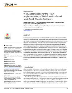
VHDL Implementation of TMDS encoder for the transmission of video signals in serial communication Supreetha Rao, Kiran Kumar V.G, Kanhu Charan Padhy Abstract— Digital visual interface transmitter and receiver in a multimedia system allow for transmitting of high definition video and audio data between the source and the receiver across a serial link at high speeds. This project highlights a detailed development of digital visual interface (DVI) transmitter and receiver in multimedia system. These include developing the architecture DVI receiver and transmitter, high speed serializer, clock and data recovery circuits and deserializer through the efficient use of FPGA resources. The project makes use of TMDS (Transition Minimized Differential Signaling) technique, that involves advanced TMDS encoding and decoding algorithms using DC balanced transmission, and helps reducing EMI over the transmission lines. Keywords —DVI, Encoder
II. PROCEDURE DVI block diagram is as shown in the fig.1 DVI cable and connectors carry four differential pair that makes up the TMDS data and the clock channels. These channels are used to carry the audio, video and the control data.
HDL. Serial Communication, TMDS
I.
INTRODUCTION
The conventional analog video graphics array (VGA) standard has been replaced by the standard digital visual interface (DVI) with the evolution of the display technology. Digital multimedia interface made use of LVDS technology, in the LVDS technology cable length was limited to short distance. The proposed work makes use of TMDS technology with TMDS encoding and decoding algorithms to overcome the drawbacks of the LVDS technology The digital visual interface (DVI) specification provides a high speed digital connection for visual data types that are display technology independently. The interface is primarily focused at providing a connection between a computer and its display device. The DVI transmitter and receiver are connected through a single or dual TMDS serial link. The TMDS link is used to send graphics data to the monitor. A TMDS link consists of a single clock channel and three data channels (RGB). The transitions minimization is achieved by implementing advanced encoding algorithm on each of the three channels, convert 8 bit of video or audio data into a 10 bit transition minimized DC balanced sequence. This advance coding algorithm enables robust clock recovery and data recovery at the receiver. Thus, it achieves greater skew tolerance for transmission over longer cable length. In the TMDS standard the type of I/O logic, which is CML (Current Mode Logic circuit), is also included hence the name “TM” due to the encoder/decoder and “DS” relates to the I/O circuit.
Fig.1. DVI block diagram The DVI system consists of a transmitter and receiver, the transmitter encodes and serially transmits a digital data stream over the twisted pair of wires to a receiver. The audio, video and auxiliary data are carried by the three data channel of the TMDS. The video pixel clock is transmitted on the TMDS clock channel and is used by the receiver as the frequency references for the data recovery on the three TMDS data channels. Each pixel has three colors, respectively, transmitting through three data channels at the same time, and each color has 8 bit source word ranging from 0-255. The encoded process for the active data can be viewed as a two stage procedure. The procedure converts 8bits per channel into the 10 bit DC balanced, transition minimized sequence which is then transmitted serially across the pair at a rate of 10bits per pixel clock period. The TMDS Clock channel carries a character ratio frequency reference. The receiver/decoder produces bit-rate sample clock based upon this reference, which is adjusted for each of the data streams, enabling proper decoding.
1576 ISSN: 2278 – 1323
All Rights Reserved © 2015 IJARCET
International Journal of Advanced Research in Computer Engineering & Technology (IJARCET) Volume 4 Issue 4, April 2015 III. LINK ARCHITECTURE The fig 2 shows the TMDS link includes three TMDS Data channels and a single TMDS clock channel.
Video transmission over the TMDS channel is logically divided into an encoder, serializer and I/O circuit stage as illustrated in the figure above, the pixel data is 8 bits wide, while the control data is 2 bits wide. The encoder must produce 10-bit words from 8-bit words, which occurs only for the pixel data. For control data, fixed 10 bit data is generated. The serializer converts the parallel data to serial on all three streams and then send them out onto three channels of differential output pair CML (current mode logic) since I/O circuit is differential two wires are required for each channel.
Fig.2. TMDS link architecture . This interface specification allows for two TMDS links enabling large pixel format digital display devices. One or two TMDS links are available depending on the pixel format and timings desired. The two TMDS links share the same clock allowing the bandwidth to be evenly divided between the two links. As the capabilities of the monitor are determined, the system will choose to enable one or both TMDS links. The input stream contains pixel and control data each of 24 bits. The transmitter encodes either pixel data or control data on any given input clock cycle, depending on the state of the data enable signal (DE). At the TMDS receiver, the recovered pixel data may have transition only when DE is active. The transmitter contains three identical encoders, each driving one serial TMDS data channel. The input to each encoder is two control signals and eight bits of pixel data. Depending on the state of DE, the encoder will produce 0 bit TMDS character from either the two control signals or from the eight bits of pixel data. The output of each decoder is a continuous stream of serialized TMDS characters. IV. TRANSMITTER DESIGN
Fig.3. Transmitter design
Fig.4. Current Mode Logic The CML transmitter-receiver pair is as shown in the Fig.4. which uses an external resistor (R2) to emulate a CML pad when regular 3.3V LVCMOS I/O‟s are used instead of CML. In fig Vhigh and Vlow are represented as „1‟ and „0‟ respectively, while Vi and Vi- represent the voltages that actually reach the CML receiver. As per the arrangements shown in the figure Vi- Vdd-Vlow R2/R1, R2 Vlow results. Therefore, R2, Vi- -Vlow/ Vdd-Vi- R1. For Vdd 3.3 V. Vi2.9 V, Vlow 0.8 V. V. TMDS ENCODING ALGORITHM The TMDS converts the 8 bit input data to the 10 bit word with less number of transitions reducing the high frequency emission and also provide near perfect DC balance on the communication wires, improving the noise immunity. In the TMDS encoder the first stage is an XOR/XNOR operator which minimizes the number of transitions and the second stage is an INV/NONINV which minimizes the disparity (DC balance). The extra two bits are added at this stage of operation. The fig.5. below represents the flow chart of the encoding algorithm for the minimum transitions and low disparity. When the video data is transmitted the encoding algorithm is categorized to two stages as shown in the fig below. The encoder here decides when to invert the next data based on the running disparity between the zeros and ones. On the basis of the 10th bit depending on the encoder the necessary steps are taken at the decoder in the sink. The table.1 depicts few examples of the data taken as the input, when the data is long transition less series automatically an transition is introduced by the encoder. The 10bit data obtained is then transmitted over the serializer provide to the CML for the transmission of the data through the links.
1577 ISSN: 2278 – 1323
All Rights Reserved © 2015 IJARCET
International Journal of Advanced Research in Computer Engineering & Technology (IJARCET) Volume 4 Issue 4, April 2015
Table.1. examples of input values VI. RESULT AND ANALYSIS The VHDL code for the encoder circuit is brought out and verified for the values of the tabular column given and the waveforms are obtained for the same as given in fig. This TMDS encoder is a programmable logic component that implements the 8b/10b encoding algorithm required by the DVI and HDMI video interfaces. The design is validated in Xilinx ISIM simulator and synthesized using Xilinx ISE 13.1 Design suite.
Fig.5. Flow chart for encoding algorithm
.
1578 ISSN: 2278 – 1323
All Rights Reserved © 2015 IJARCET
International Journal of Advanced Research in Computer Engineering & Technology (IJARCET) Volume 4 Issue 4, April 2015 REFERENCES [1] Digital Visual Interface, Revision 1.0, Digital Display Working Group, http://www.ddwg.org. [2] Design and implementation of high definition multimedia interface transmitter and receiver, International Journal of Advanced Technology & Engineering Research (IJATER) [3] Al Widmer, Peter Franaszek, ―A DC-Balanced, Parti-tioned-Block, 8B/10B Transmission Code‖ IBM [4] Journal of research and development, Volume 27, Number 5, Septem-ber 1983.
1st Author : Ms. Supreetha Rao, recieved her B.E degree in electronics and communication engineering from Sahyadri College of Engineering & Management in 2011 and currently pursuing her M.Tech in VLSI & Embedded Systems in Sahyadri College of Engineering & Management. She has interest in the field of design for low power circuits, VLSI digital system and communication system. She has published one paper in IJAEM journals another in IJSR and have two years of teaching experience in the Sahyadri college of Engg. She is presently, engaged in the prototype design & development of Digital System at KCTRONICS Innovative Consultancy Services Private Limited on internship as a part of M.Tech curriculum..
Mr. Kiran Kumar.V.G has done his B.E and M.Tech in Microelectronics in NMAMIT, Nitte. He
has
secured
third
rank
in
M.Tech
(microelectronics & control system) in V.T.U. He has got 11yrs of experience in teaching profession.
Shri Kanhu Charan Padhy, has been graduated from UVCE, B.U, Bangalore (Electronics). He has done his PGDBA in HRM&Finance. He has served in DGAQA, Govt. Of India as a Group „A‟ Officer. He has published some articles like „Quality in Design and Reliability through Repair‟ in the Quality Focus Journal of ADE, DRDO. He has published one paper in the National Conference on” Ground and Flight Test of Systems Used in Military aircraft” at NaSMAC-2004.20-21 August 2004,, Bangalore & another paper in the International Conference on “QMS (9001/2000) Implementation –A boon to the Industries” at ConQuest-2006, International Conference on Quality & Reliability in Aerospace Systems, Jan15-17, 2006. Organized by RCI, DRDO, Hyderabad..He has been declared as the Best Citizen of India during 2003.He has been awarded with Commendation by the Gp Capt. P.Kamraju. He has served as a guide for the management students in the field of finance. Presently he is the M.D of KCtronics Innovative Consultancy Services private Ltd., Professional Membership: SAQR (The Society for Aerospace Quality & Reliability) : Life Membership #LM192
1579 ISSN: 2278 – 1323
All Rights Reserved © 2015 IJARCET