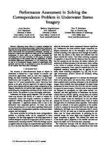
Comparing the Performance of FPGA-Based Custom Computers with General-purpose Computers for DSP Applications Neil W. Bergmann and J. Craig Mudge CSIRO/Flinders Joint Research Centre in Information Technology Flinders University, GPO Box 2100, Adelaide, SA 5001, AUSTRALIA Tel: 61-8-201-3109; Fax: 61-8-201-3507 E-mail:
[email protected],
[email protected] conventional desktop workstations, and often significantly greater than the best reported results using "conventional" super-computers, especially for those algorithms which can be decomposed into many, simple, parallel processing tasks. Many Digital Signal Processing (DSP) algorithms can be decomposed into parallel tasks, but each task often involves relatively complex operations such as a multiply-accumulate. DSP algorithms are therefore less clearly suitable candidates for efficient implementation on a custom computer. This paper surveys some of the most important custom computers, presents the authors' work on a new custom computing architecture specifically designed to support DSP applications, and analyses the performance of various implementation alternatives for DSP algorithms.
Ab stract When FPGA logic circuits are incorporated within a stored-program computer, the result is a machine where the programmer can design both the sofhvare and the hardware that will execute that software. This paper first describes some of the m r e important custom computers, and their potential weakness as DSP implementation platforms. It then describes a new custom computing architecture which is specifically designed for efficient implementation of DSP algorithms. Finally, it presents a simple performance comparison of a number of DSP implementation alternatives, and concludes that (i) the new custom computing architecture is worthy of further investigation, and (ii) that custom computers based only on FPGA execution units show little performance improvement over state-of-the art workstations.
2. Previous methods of customising computers for DSP
1. Custom computing Field Programmable Gate Arrays are now a popular implementation style for digital logic systems and subsystems [l]. Where the programming configuration is held in static RAM,the logic function implemented by those FPGAs can be dynamically reconfigured, in fractions of a second, by rewriting the contents of the S R A M configuration memory. When such P G A logic circuits are incorporated within a stored-program computer, the result is a machine where the programmer can design both the software and the hardware that will execute that software. Such a machine, where the hardware can be reconfigured and customised on a program-by-program basis, is called a custom computer
There is a constant tension in computer design between being general purpose, i.e., doing a wide range of computational tasks moderately well, and being application specific, i.e., doing a smaller range of computational tasks much better, usually at the cost of either increased system resources or of poorer "general purpose" performance. There have been many different approaches investigated over the years for improving the performance of a general purpose computer for the implementation of DSP algorithms. Custom computers represent the latest technology which shows some promise for this task. A common approach to improving the performance of a general purpose computer for specific applications is the addition of application specific hardware, such as
PI. Several researchers report algorithm speed-up rates of hundreds or thousands of times compared to
164
0-8186-5490-2/94 $03.000 1994 IEEE
graphics accelerators for computer displays, or image and video compression chips for multi-media workstations. These can provide excellent speedup for that specific application, but provide no performance improvement when other applications are run. This approach represents one extreme of the generality/cost spectrum. Another common approach, at the opposite end of the spectrum, is the addition of a general-purpose parallel processing sub-system to a host processor. Such add-on parallel processing boards have seemed an obvious and attractive enhancement to desktop computers for some time, but they have achieved only limited success in the marketplace. It is our conjecture that this is because of difficulty of programming, and high cost resulting from low sales volumes. Additionally, such parallel processing systems have commonly been inefficient at implementing the fine-grain, communications-intensive parallel algorithms associated with DSP applications. Recently, general-purpose, Digital Signal Processor chips such as the TMS32OC40 [3] have become available. These combine high speed, floating-point arithmetic performance with high speed interprocessor communication channels incorporating individual DMA controllers. Arrays of such chips provide a formidable challenge for other DSP implementation altematives. The idea of a computer which can be customised, under programmer control, on an application-byapplication basis, is not new. A writable control store within a micro-programmed computer allows the programmer to design application-specific machine instructions, which can make better use of the existing functional units within the computer, and hence improve the performance of specific applications, including those within DSP [4]. Such performance improvement has been limited because of the interpretative nature of microprogramming. A custom computer goes one step further than a writable control store by allowing design of new functional units, rather than simply making better use of existing functional units.
boards, with each board containing 16 Xilinx 4010 FPGAs [6], connected as a linear array, plus an extra Xilinx 4010 for control, with all of the FFGAs having some additional interconnections via a central crossbar switch. The SPLASH boards can communicate with a SUN Sparcstation host via input and output FIFOs, which are on an additional interface board connecting the SUN and SPLASH array. Once configured, data is streamed through the SPLASH processor using the systolic array programming model, with results streaming back to the host. The SPLASH processor is most suited to simple streaming operations, and has shown significant speedups over conventional supercomputers for tasks such as text searching and genetic database searching. SPLASH is usually programmed by specifying the function of the FPGAs using VHDL, which is then automatically translated into an FPGA configuration file. Current research [5] is examining the use of other programming languages, such as data parallel C.
3.2 Programmable Active Memory The PAM (Programmable Active Memory) has been under development at DECs Paris Research Labs for several years [7], [8]. The latest version, PeRLe-1, consists of a 5x5 array of Xilinx 3090 FTGAs, connected to local 32-bit wide RAM banks, and also, via a lOOMB/s TURBOchannel interface, to a DEC desktop workstation. The workstation writes data to the RAM banks, which is processed by the Xilinx array and returned to the RAM banks, from where the host then retrieves the results. Programming the PAM consists of designing software components for the host, and hardware components for the PAM array. The latter can be done by writing a program in a conventional programming language (Lisp, C++, and Esterel are used) using a specialised library. The program describes logic modules by their bit-level logic equations, or by using standard library modules such as adders, and registers. Ten applications are described in [8], including long multiplication, RSA cryptography, data compression, string matching, heat and Laplace equations, a Boltzmann machine neural network, 3-D graphics acceleration, and the discrete cosine transform. Results are very encouraging; e.g., the PAM implementation of 512-bit RSA cryptography was faster than any other reported implementation in any technology as of February 1990, and 10 times faster than the next best reported implementation on a custom VLSI circuit.
3. Some Existing Custom Computers In this section, we examine three of the best known custom computers as examples of the current state of the art in this area.
3.1 SPLASH SPLASH and SPLASH I1 [ 5 ] are custom computers which have been developed at the Supercomputer Research Corporation, Maryland. The SPLASH I1 processor consists of an extendable number of processor
165
3.3 The Virtual Computer
cessing element. For this reason, we are now exploring a new custom computing architecture explicitly targetted at the efficient implementation of digital signal and image processing applications.
The Virtual Computer [9], from the Virtual Computer 500,000 Corporation, provides approximately programmable logic gates, using an array of 52 Xilinx 4010 FPGAs and 24 ICUBE Field Programmable Interconnect Devices, 8 megabytes of SRAM, and 16k x 16-bit 25ns dual-port RAMs. The system also has 3 x 64-bit 1/0ports - one for hardware configuration / readback, and two for general purpose 1/0 such as connection to a host workstation. The central processing array of 40 Xilinx FPGAs, called the Virtual Array, consists of four Virtual Pipelines, each with 10 FPGAs connected to dual-port RAMs at each edge of the pipeline, with the other port of these dual-port RAMs connected to a control FPGA with a RAM buffer. The array is intended to be a flexible computing resource, with a typical application on a host processor loading data into SRAM, which is streamed through the pipeline under local control via the dual-port RAMs. Results would take the reverse route back to the host. All of the FPGAs are designed to be reprogrammed in parallel, so that the function of all 500,000 logic gates can be changed in 25 ms. It is intended that programming could be at several levels. At the highest level, a run-time function library would be provided. Next would be translation of VHDL or C++ code into hardware implementations, and at the lowest level would be full-custom hand placement and routing. The Virtual Computer is interesting in that it is designed as a commercial product (initially targetted at the research community), rather than as a research vehicle.
4.2 Our New Architecture Our decision to concentrate our efforts on a custom computing architecture which is specifically designed for the support of DSP algorithms leads us naturally to the provision of specific hardware support for the arithmetic operations which dominate many DSP algorithms, but which are costly to implement using FPGA programmable gates. Our proposed architecture has developed from previous work into the rapid prototyping of DSP algorithms [ lo]. An experimental system was built from an Algotronix CHS2x4 (Configurable Hardware System) Ell] PC plug-in board containing 8 CAL1024 chips and 512 kbytes of RAM, plus a second plug-in board with 4 custom VLSI chips, each containing four 16-bit, bitserial multiply-accumulate units. The major drawback of our initial architecture is its reliance on a customdesigned arithmetic resource chip. Our limited design and fabrication budget means that such chips have only moderate arithmetic performance, and even a small array of such chips will at best be able to match the arithmetic performance of modem CPU chips. Attempts to code up simple DSP algorithms for this system, such as FIR filters, have also demonstrated weaknesses in the data transfer capability of the CHS2x4 system for communications-intensive applications. We have therefore commenced work on a more ambitious architecture [12], which more closely couples an arithmetic chip, static RAM, and reconfigurable logic within a processing node as shown in figure 1. This node is then replicated a number of times to produce a complete custom-computing co-processor for a workstation. It seems likely that this architecture will use commercially available arithmetic chips, providing of the order of 20 MFLOPS each. Eight such processing nodes would give some 160 MFLOPS of processing power. The architectural and algorithmic challenge then becomes to ensure that the reconfigurable logic chips and static RAM chips can store, communicate and organise operands for these arithmetic chips to allow such a peak processing performance to be sustained. It is useful to review our progress in the design of such a custom computer in the light of the other custom computing projects underway internationally. In particular, this paper examines whether such an architecture does give some performance advantage compared to the more general-purpose custom computing
4. CC-DSP: A New Custom Computer 4.1 Weaknesses of Existing Custom Computing Architectures for DSP It is useful to examine those applications where custom computing has shown the greatest speedups. In general, such applications can be decomposed into many parallel computations, each of which can be implemented by a low-gate-count processing element. Thus many such elements are able to be implemented on the available FPGA resources of a custom computer. Typical applications in this category include text searching and genetic database matching. DSP applications often exhibit a high degree of potential parallelism, but are less suitable for implementation on a custom computer because of the high gate count of the arithmetic operations (addition and multiplication) typically required for each parallel pro-
166
Data from column neighbour
Aritmetic Chip
Data from row ReconfigurableLogic Chip neighbour Data from RAM Data to RAM
I I
RAMChip
1 \1 I
Data to row neighbour Data to column neighbour
Figure 1: A new custom computing architecture showing (a) processing node structure, and (b) processing node interconnection. architectures described above, for the specific application area of digital signal processing.
5.2 TMS320C40 Parallel Processing Development System
5. Other Computing Architectures for DSP
The TMS320C40 [3], with a clock rate of 40MHz, is indicative of the current state-of-the-art in softwareprogrammable digital signal processor chips. Important features of the TMS32OC40 are the ALU design, and the interprocessor communications design. The ALU is based on a single-cycle floating-point unit, which has separate multiplication and addition units to allow these two operations to be done in parallel. Single-cycle operation eases programming of inner loops compared to the Alpha's highly-pipelined unit. Peak arithmetic performance is then 80 MFLOPS, with a 40 MHz clock. The TMS320C40 also has six, byte-wide, bidirectional interprocessor communications ports with a transfer rate of 20 Mbytesh each. Each port has a dedicated DMA controller, which relieves the CPU of much of the burden associated with the high interprocessor communications in fine-grained, parallel DSP algorithms. Texas Instruments market a parallel processing board based on the TMS32OC40, called the Parallel Processing Development System (PPDS) [3], which can be attached to a general purpose workstation. The TMS-PPDS contains 4 interconnected TMS32OC40 chips, plus global and local memory banks. Its peak arithmetic computation rate is then 4 * 80 MFLOPS = 320 MFLOPS. The PPDS will be used as an element of the performance comparison in the next section.
To use for later comparison two more conventional DSP implementation methods are briefly described below.
5.1 Alpha-basedworkstation. Digital Equipment Corporation's Alpha 21064 processor chip [l5], with a system clock rate of 200 M H z , is indicative of the current state of the art in desktop workstation performance. The 21064 chip also forms the basis for the recently announced massivelyparallel processing (MPP) supercomputer from Cray Research, Inc [ 151. Of particular interest here is the excellent arithmetic performance of the processor. The 21064's pipelined ALU can accept new operands on every clock cycle, with a ten-cycle latency before results appear. It is reasonable to assume that careful coding of DSP inner loops to maximise pipeline occupancy is no more difficult than custom computer hardware design. The peak floatingpoint (or integer) computation rate is then 200MFLOPS. This rate would require operands to be available in registers, and instructions to be available in the cache to be sustained. Assumptions about a suitable sustained computation rate for comparison with custom computing approaches are given later.
167
6. Performance comparison of programmable DSP Architectures
the various alternatives and we have not measured the actual performance of any of the systems. Performance is described in terms of millions of multiply-accumulate operations per second (megaMAC/s) for the case of both floating-point and fixed-point arithmetic, for each of the "single-boardsized systems. An attempt is also made to calculate the cost of each board, using a simple measure of "number of chips" as the cost. This gives the performance measure of megaMAC/s/chip. For this measure, only processing and interprocessor communication chips are counted. Memory chips, and host-interface chips are not counted. Details of the individual performance calculations are given in section 6.4, below.
As mentioned previously, the high logical complexity of the arithmetic operations which are central to many DSP algorithms suggests that FPGA-based custom computers may be less suited to the implementation of such algorithms compared to their demonstrated performance speedups in other areas. We therefore present a simple performance analysis of some DSP implementation alternatives, to test this assertion. The two key questions in any performance comparison are what to compare, and how to compare them. 6.1 What to Compare?
6.3 Assumptions
We have chosen to compare DSP implementation systems which are of the order of a single printed circuit board, and which might be used to improve the DSP performance of a desktop computer workstation. The following six systems will be compared. Slate-of-the-Art Custom Computers (i) A single SPLASH II processor board. Results for multiboard systems can be extrapolated from this result. (ii) The DEC PeRLe-1 system (iii) The Virtual Computer Specialised DSP Custoni Computer (iv) CC-DSP: The new (yet to be built) custom computer described in section 4.2 above is used, referred to as CCDSP in this paper. We assume it consists of 8 PE's, each containing one RAM chip, one arithmetic chip, and one reconfigurable logic chip. For the arithmetic chip, we assume an arithmetic perform'mce of one floating-point multiply-accumulate every lOOns can be sustained, which is consistent with existing state-of-the-art ALU chips (e.g. [ W . General-purpose Processors (v) A TMS-PPDS consisting of four TMS32OC4Os. (vi) A workstation using a 2OOMHz DEC Alpha 21064 processor.
Assumption 1. The limiting factor in DSP performance is the computation of multiply-accumulate operations, which dominate many DSP algorithms, such as digital filters, linear transforms, matrix multiplications, and artificial neural networks. Assumption 2. For the previously-mentioned conventional custom computing architectures, which all use Xilinx FPGAs, the cost of a fixed-point multiplication is based on a recent design by Casselman [13]. This 24-bit fractional multiplier requires 48 CLBs (configurable logic blocks) within a 4000 series Xilinx FPGA, and produces a result in 16 clock cycles at 16 MHz. We assume that a fixed-point addition can be done in the Same time using an extra 2 CLB's for a total of 50 CLB's for a fixed-point multiply-accumulate operation, at 1 million operations per second. Assumption 3. For the same conventional custom computing architectures, the cost of a floating-point multiplication is based on the same design by Casselman [ 131. A single-precision floating point multiplier requires 60 CLBs within a 4000 series Xilinx FPGA, and produces a result in 16 clock cycles at 16 MHz. We estimate, given some experience with previous floatingpoint operator designs [14], that a floating-point adder requires a similar-sized circuit to a floating-point multiplier, which would give a total of 120 CLB's for both. We can assume some saving for a combined floating-point multiply-accumulate operator, and so we will assume 100 CLB's are required. Operating speed is again 1 million operations per second. Assumption 4. For the same conventional custom computing architectures, it is assumed that 25% of chip area is required for control, and other overhead hardware such as multiplexers and registers. Most of the systems described use Xilinx 4010 FPGAs, with 400 CLB's.
6.2 How to Compare Them? The goal of this analysis is to give some ballpark figures for the various DSP implementation alternatives to give some insight into their relative merit. A very straightforward analysis has been undertaken, based on a number of assumptions which are listed below. The performance analysis is a static analysis based on the stated performance of various components. We have not implemented any benchmark algorithms on
168
(fixed-point) and 75/40 = 1.9 megaMAC/s/chip (floatingpoint).
Accounting for the 25% overhead leaves 300 CLB's for the multiply-accumulate operations. Hence we assume that a Xilinx 4010 can provide a performance of 6 megaMAC/s (fmed-point) or 3 megaMAC/s (floatingpoint). We further assume that the Xilinx 3090s used in the DEC PeRLe-1 can provide the same performance. Assumption 5 . For our new CC-DSP architecture, we assume 8 processing nodes, where each node is provided with a custom arithmetic support chip providing 10 million multiply-accumulate operations per second (80 million multiply-accumulate operations per second for the system). We assume that the reconfigurable logic chips in the system are used to control data flow to ensure that the FPUs are kept busy, but do not provide any additional multiply-accumulate resources. Assumption 6. For the DEC Alpha 21064 workstation, Linpack 1OOOxlOOO results [15] suggest a best-case sustained computation rate of 75% of the peak rate. Reducing this to 50% to account for general algorithm and system overheads, this gives 50 million multiply-accumulate operations per second. A nominal chip count of 10 is assigned to the Alpha-based workstation to account for the support chips needed for this processor. Assumption 7. The TMS-PPDS has a peak processing rate of 4 * 80MFLOPS (each chip can do parallel floating-point multiply and add operations at 40 MHz). Since the processors have to deal with overhead instructions, as well as the floating-point operations, we suggest the same average floating-point computation rate as in assumption 6, i.e., 50% of the peak.
Virtual Computer: The Virtual Computer contains a total of 52 Xilinx 4010 FPGAs and 24 ICUBE FPICs, 8 megabytes of SRAM, and 16k x 16-bit 2511s dual-port RAMS. 40 Xilinx chips are available for arithmetic operations, giving 40*6 = 240 megaMAC/s fmed-point, and 40*3 = 120 megaMAC/s floating-point. The cost of the system is considered to be 52+24 = 76 chips, giving performance of 240/76 = 3.1 megaMAC/s/chip (fixedpoint) and 120/76 = 1.6 megaMAC/s/chip (floatingpoint). CC-DSP: Our new custom computing architecture for DSP has 8 nodes, with each node consisting of one FPGA, one arithmetic chip of 10 megaMAC/s performance, and one RAM chip. Total performance is then 80 megaMAC/s, fixed- or floating-point. Cost, excluding RAM, is 16 chips, giving 5 megaMAC/s/chip, fixed- or floating-point. TMS-PPDS: The peak performance of the 4-processor system is 4 * 40 = 160 megaMAC/s. With a sustained rate of 50% of the peak this gives 80 megaMAC/s. Examination of the PPDS shows about four extra support chips (excluding RAM) for each processor chip, giving a total cost of 20 chips, and hence 4 megaMAC/s/chip fixed- or floating-point. Alpha 21064 Workstation: The peak performance of this system is 200MFLOPS = 100 megaMAC/s. With a sustained rate of 50% of the peak this gives 50 megaMAC/s. With a nominal workstation motherboard cost of 10 chips (excluding RAM), this gives 5 megaMAC/s/chip fixed- or floating-point.
6.4 Performance and Cost Estimates SPLASH II: A SPLASH I1 board consists of 16 Xilinx 4010 chips, a crossbar switch controlled by another Xilinx, plus some memory and interface circuitry. The 16 Xilinx chips provide 16*6 = 96 megaMAC/s fixed-point, and 16*3 = 48 megaMAC/s floating-point. The cost of the system is considered to be the 16 FPGAs plus another 16 chips for the crossbar switch and its control, giving a total cost of 32 chips. Performance/cost is 96/32 = 3 megaMAC/s/chip (fixed-point) and 48/32 = 1.5 megaMAC/s/chip (floating-point).
These calculations are summarised in Table 1 below.
6.5 Conclusions Two conclusions can be drawn from the above, simple analysis. The first is that our CC-DSP architecture gives a moderate performance improvement over other custom computing approaches for floating-point DSP applications, on a computation-per-chip basis, and so is worthy of further investigation. There is an insignificant (in terms of the resolution of this analysis) performance improvement for fixed-point DSP operations. The second conclusion is that, for DSP applications, single-board custom computing approaches (including our CC-DSP) do not give any performance/cost
DECPeRLe-1: The DEC P e w - 1 co-processor board consists of 25 Xilinx 3090 chips for the programming core, four RAM banks, plus additional FPGAs and logic circuits to control the RAM banks and general purpose interconnect. The 25 Xilinx chips provide 25*6 = 150 megaMAC/s fixed-point, and 25*3 = 75 megaMAC/s floating-point. We assign a total cost of 40 chips, giving performance/cost of 150/40 = 3.75 megaMAC/s/chip
169
I
System
SPLASH I1 board DECPeRLe-1 Virtual Computer Our CC-DSP TMS-PPDS Alpha Workstation
# of chips (# of Xilinx)
I 32 (16) 40 (25) 76 (40) 16 20 10 {nominal)
megah4ACIs (fixed-point)
megah4ACIsl chip (fixed-point)
megah4ACIs (floating-point)
megaMACls1chip (floating-point)
96 I96 150 I 150 240 1240 80 1 80 801 160 5 0 / 100
3 3.75 3.1 5 4 5
48 I 48 75 I 75 120 1 120 80 I 80 801 160 501 100
1.5 1.9 1.6 5 4
5
(c) discern a demonstrably scalable design which can utilise the technology progress function of the individual components of our CC-DSP architecture.
improvement over the conventional parallel processing and uniprocessor approaches. The major reason for this is that both the TMS32OC40 and Alpha 21064 have high-performance hardware support for floating-point arithmetic. Custom computers provide the best speedups compared to conventional workstations when they can implement in parallel hardware what the workstation needs to implement in serial software. DSP does not immediately appear to be such an application area. The reason for the poor performance of the CC-DSP architecture is the unavailability of single chip ALVs which can match the floating-point performance of modem processors. The single-chip ALUs are largely limited by their ability to transfer operands and results to and from the chip, compared to the processors whose ALUs transfer data to and from local registers. Finally, a general comment on the long-term sustainability of special purpose, or custom, architectures The TMS-PPDS and the Alpha can be made. workstation described here are both general purpose systems. Hence their technology progress functions will approximate that of logic technology. The new custom computing architecture presented here, because it is special purpose, will be manufactured in lower volumes and hence will tend to have a less steep technology progress function. Thus, it will be challenging for the custom architecture to sustain a competitive position. It is necessary that the arithmetic, SRAM and FPGA operand-handling components have the same slope of progress function as the general purpose systems. Furthermore, we require that the operand handling architecture built from FPGAs be scalable, so as to avoid a data communications bottleneck which will prevent full utilisation of the technology progress functions of these individual components. We plan further work in this area to: (a) get better performance measures than those used in the simple analysis presented in Table 1, (b) decide on the best method to provide arithmetic resources for DSP within a custom computing architecture, and
7. Acknowledgments This work is supported by the Australian Research Council under Grant A49132307. Thanks to Lui Cirocco for his assistance in the design of our next generation CC-DSP architecture.
References J. Rose, A. El Gamal, and A. Sangiovanni-Vincentelli, "Architecture of Field-Programmable Gate Arrays," Proceedings of the IEEE, 81(7), July 1 9 9 3 , 1013-1029. ~~ Proceedings of IEEE Workshop on FPGA's for Custom Computing Machines, Napa, April, 1993. TMS320C4x Technical Brief, Texas Instruments, 1991, pp 6.5-6.8 L. R. Morris, and J.C. Mudge, "Speed Enhancement of Digital Signal Processing Software via Microprogramming a General Purpose Minicomputer," Proceedings of ICASSP '77, 1977. M. Gokhale, R. Minnich, "FPGA Computing in Data Parallel C," Proceedings of IEEE Workshop on FPGAs for Custom Computing Machines, Napa Valley, April, 1993. The XC4000 Data Book, Xilinx, Inc., San Jose, 1992. P. Bertin, D. Roncin, J. Vuilemin, "Introduction to Programmable Active Memories", DEC Paris Research Labs, Research Report #3, June, 1989. P. Bertin, D. Roncin, J. Vuilemin, "Programmable Active Memories: a Performance Assessment", DEC Paris Research Labs, Research Report #24, 1993.
170
[14] D. Giarola & N.W. Bergmann, "Design and Testing of a Bit-Serial Floating Point Adder", & "Design and Testing of a Bit-Serial Floating Point Multiplier", University of Queensland, Electrical Engineering Dept., Internal Reports No. EE8915 & EE89l9, May, 1989. [15] E. McLellan, "The Alpha AXP Architecture and 21064 Processor", IEEE Micro, 13(3), June 1993, ~~36-47. [16] M. Birman, A. Samuels, G. Chu, T Chuk, L. Hu, J. McLeod, J. Barnes, "Developing the WTL3 170/3171 Sparc Floating-Point Coprocessors", IEEE Micro, 10(1), pp. 55-65, February, 1990.
[9] S . Casselman, "Virtual computing", Proceedings of IEEE Workrhop on FPGA's for Custom Computing Machines, Napa Valley, April, 1993. [lo] N.W. Bergmann, H. Wong, P. Sutton, "A Rapid Prototyping and Implementation Method for Systolic Array Digital Signal Processors", Proceedings of 1991 Microelectronics Conference, Melbourne, pp 91-93, 1991. [ 113 CHS2x4 User Manual, Algotronix Ltd, Edinburgh, Scotland, February, 1992. [12] N.W. Bergmann, J.C. Mudge and L.R. Cirroco, "FPGA-Based Custom Computers", 1993 Australian Conference on Microelectronics, Gold Coast, October 1993. [ 131 S . Casselman, "F'PGA multiplier", info-fpga electronic mail posting fi-om
[email protected], October, 1993.
171