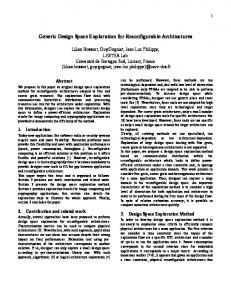
Proceedings of the 38th European Microwave Conference
Design of a Broadband MEMS-based reconfigurable coupler in Ku-band Luca Marcaccioli#1, Paola Farinelli#2, Manos M.Tentzeris*3, John Papapolymerou*4, Roberto Sorrentino**5 #
RF Microtech s.r.l., Via G. Duranti, 93, 06125, Italy
{1marcaccioli, 2farinelli}@rfmicrotech.com *
GEDC, School of ECE, Georgia Institute of Technology, Atlanta, GA 30332-250, U.S.A 3
4
{ etentze, papapol}@ece.gatech.edu **
University of Perugia, Dept. of Electronic and Information Engineering, Via G. Duranti, 93, 06125, Italy 5
[email protected]
Abstract — A broadband reconfigurable coupler has been realized at Ku band making use of RF-MEMS switches. The coupler is directly printed on the same Silicon substrate on which the MEMS are built. The device works at 16-20 GHz, and it is designed to provide two different coupling levels of -10dB and -17dB, maintaining good matching and isolation in both states. Performance significantly matches the simulations, verifying how close the MEMS switches perform to the predicted behavior. This also demonstrates that the MEMS fabrication process is repeatable and predictable.
I. INTRODUCTION Nowadays reconfigurable devices play a very important role in communication systems as they enable the possibility to add functionalities and improve the performance of many apparatus while lowering the equipment costs. In particular the emerging technology of RF-MEMS will have a key role in the near future, since it can facilitate the fabrication of highperformance reconfigurable devices that can be used up to mm-wave frequencies without any increment on complexity of the manufacturing process. Also, RF-MEMS devices are today approaching a certain degree of technological maturity: although still being affected to a certain extent by reliability issues, these devices present excellent performance in terms of loss and linearity, and overall maintaining low fabrication costs. In this paper we present for the first time a MEMS-based reconfigurable coupler. The circuit is based on a novel architecture presented in [1]. Specifically, these types of device can provide two or more coupling levels while maintaining good matching and isolation in all states. In the past, many devices with similar functionalities have been presented, although nearly none of them making use of MEMS. Reconfigurable couplers have been proposed in waveguide technology [3]-[4], while in [5]-[7] two versions of planar analogue reconfigurable couplers employing varactors have been presented. In [8]-[12] several schemes of reconfigurable power divider/combiners have been also introduced. The only example of reconfigurable power divider/combiner using MEMS has been presented in [2]. In that case, the circuit is made by two hybrid couplers and a phase-shifter, this resulting in a pretty large architecture with
978-2-87487-006-4 © 2008 EuMA
high loss. In comparison, our MEMS-based coupler has very low-loss and approximately the same size of a conventional quarter-wavelength coupler. Applications range from AGC (Automatic Gain Control) devices to measurement tools, from variable attenuators to dual-state amplifier schemes, as well as RF modulators and reconfigurable feeding networks. As stated before, in [1] the first demonstrator of reconfigurable coupler has been fabricated and measured; in that case PIN diodes were used for demonstration purposes, and the device worked at 5 GHz. In this paper a new device based on RF-MEMS and working at 18 GHz with 20% fractional bandwidth has been fabricated and tested. The circuit shows good performance and above all the measurements show an excellent repeatability and predictability. In addition, results show that the fabrication process employed is now mature. In Sec. II, the design of the coupler is briefly described; in Sec. III, the technology used for MEMS is discussed. Sec. IV reports the measurements of the device, along with the difficulties encountered while Sec. V draws some conclusions and illustrates thoughts for future work. II. COUPLER DESIGN The design is based on the properties of three coupled lines of unequal impedance, whose total length is a quarter of a wavelength; with reference to Fig.1, the coupler has four ports located at the extremities of two side lines (line 1 and 3). The circuit is symmetrical, i.e. port 1-2 are the same of ports 3-4. When both switches are disconnected (ideally providing an open circuit), line 3 and line 1 are weakly coupled, since their mutual capacitance is the series of C12 (mutual capacitance between line 1 and 2) and C23 (mutual capacitance between line 2 and 3). On the other hand, when both switches are connected (ideally a short circuit), the coupling between line 1 and 3 is only given by C12 and it is therefore stronger. An ideal reconfigurable coupler would have in both states a perfect matching and an infinite directivity. Once the two levels of wanted coupling are specified, this is obtained by optimizing the geometry of the coupler: the widths of the three lines (i.e. their impedance), the two input admittances Ga and Gb, and the
595
October 2008, Amsterdam, The Netherlands
Authorized licensed use limited to: Georgia Institute of Technology. Downloaded on November 30, 2009 at 00:31 from IEEE Xplore. Restrictions apply.
gap width among line 1-2 and 2-3. The formulas given in [1] are to be used to such purpose. However, we found that a physical solution to this problem exists only if a finite directivity and a reasonable mismatching can be accepted. In other words, the proposed reconfigurable coupler cannot in principle exhibit an ideal behaviour that is, anyhow, not required in most practical cases. Once optimized, the reconfigurable coupler can provide two distinct coupling levels yet maintaining a good matching and directivity in both states. Also more than two states can be obtained, by cascading more sections similar to the one described, and maintaining an overall length of a quarter of a wavelength (or odd multiples).
3 1 4 a)
2 Simulations 0 Coupling state 2 (switches ON): -8 dB -10 Coupling state 1 (switches OFF): -16 dB -20 -30 -40 16
b)
Reflection coefficient 1 and 3 (worst case )
17
18
19
20
Frequency (GHz)
Fig. 2a) Layout (Agilent ADS) of the microstrip coupler employing RF MEMS switches and operating at 18 GHz. 2b) Simulations, coupling levels obtained with the switches both in the ON and OFF state. Reflection coefficient refers to the worst case of the two simulations.
Fig. 1. Scheme of the 1-bit reconfigurable coupler employing two switches
This approach has been followed to design a 1-bit coupler working at 18 GHz, using two MEMS switches as tuning elements. The switches are similar to the ohmic contact cantilever beams presented in [13] and better illustrated in the next section. The entire circuit was entirely manufactured on HR (High resistive) Silicon at FBK-RST (Trento, Italy). Fig. 2a shows a sketch of the device. In this prototype we have chosen not to vary the impedances of the four ports, that have been set to 50 Ohm. The coupler has been therefore optimized for a good input reflection loss at port 1 (and 3), whereas lesser weight has been given to the reflection loss of port 2 (and 4). In many practical applications in fact the input matching at the coupled line (i.e. port 2 and 3) is not a critical parameter, for instance if the coupler is used in a preferred direction (e.g. in receiving-only or transmission-only circuits) or when used in combination with amplifiers. Fig. 2b shows the simulations obtained with ADS Momentum. The two chosen coupling states are -8 dB and -15 dB. The matching obtained at the input of line 1 is better than -20 dB. Isolation and return loss at port 2 (and 4), not shown in the figure, are in both states better than 15 dB and 8 dB, respectively. The simulations have been performed including MEMS switches and biasing lines in the circuit. It shall be observed however that the biasing lines have been realized in high-resistive poly-silicon; their effect at RF is therefore negligible.
III. MANUFACTURING AND SWITCH CHARACTERIZATION The coupler has been manufactured on 525 μm thick HR silicon substrate by using the FBK-irst MEMS process described in [13]. The MEMS switches consist of a 1.8 μm thick cantilever gold beam (110 μm wide and 190 μm long) anchored at line 3 of the coupler (see Fig. 2a). The switch actuation is obtained by applying a voltage difference between line 3, and the actuation pads placed below the MEMS bridge. The electrical contact with line 2 is provided by the beam flexion on seven bumps placed in the contact area, which consist of small poly-silicon pillars placed underneath. The dimples have been covered with a gold cupping in order to obtain a low resistance gold-to-gold contact between the beam and the line. In addition the beam has been reinforced with 4 μm thicker gold in its central part so that the applied force can be better controlled by bending of the cantilever tip. In order to test the performance of the single MEMS switch, it has been designed and fabricated in series of a 1.3 mm long 50 CPW line and measured on wafer. Figs 4 shows the measured and simulated S-parameters of the switch, the latter being obtained by equivalent circuit simulations of the ideal switch (no contact resistance and bias lines are considered).
596 Authorized licensed use limited to: Georgia Institute of Technology. Downloaded on November 30, 2009 at 00:31 from IEEE Xplore. Restrictions apply.
IV. MEASUREMENTS
Fig 3 MEMS cantilever switch
0.0 -0.5
-20
-1.0
-30
-1.5
-40
-2.0
-50
-2.5
-60
Insertion Loss [dB]
Return Loss [dB]
0 -10
-3.0 0
5
10
15
20
25
30
20
25
30
freq, GHz
Isolation [dB]
0 -20 -40 -60 -80 0
5
10
15 freq, GHz
Fig.4. Comparison between measured (red curve) and simulated (blue curve) performance of the MEMS cantilever switch. (a) switch in on-state; (b) switch in off state.
Excellent and extremely wideband performance has been obtained in the tested frequency band 0-30 GHz. The comparison with the simulated ideal switch allows estimating a switch contact resistance of less than 1 Ohm, resulting in a switch insertion loss better than 0.2 dB @ 20 GHz. The line loss contribution was about 0.1 dB at this frequency. Isolation better than 20 dB has been measured in the 0-20 GHz frequency band, corresponding to an off-state capacitance of about 8 fF. Actuation and de-actuation voltages of about 50 V and 40V have been recorded. These values are slightly higher than the computed ones. Optical profile inspections showed indeed that the cantilever tip is 2 μm upward bended due to residual stress of the double layer gold beam. This explains the higher actuation voltage but do not prevent the switch from realizing a very good ohmic contact when activated. The measured actuation time is 40 μs for 50V applied voltage.
Figs. 5-7 show a picture of the fabricated device, with the proper text-fixture for measurements. Fig. 7 depicts the measurements (solid line): the S11 at port 1 and 3 is below -10 dB within the considered frequency band. The obtained coupling is -10 dB in one state and -17 dB in the other one. Isolation is -13 dB and matching of port 2 and 4 is 6 dB (not shown in the figure). As illustrated in the previous section, the actuation voltage of the switches is around 50 V for both of them. The differences with simulations of Fig. 2b can be ascribed to two main reasons, hereafter described. The measurements have been taken by using a bulky ad-hoc text-fixture, holding four SMA connectors that are directly laid over the microstrip lines (Fig. 6). This transition, within the band of interest, introduces parasitic (series inductance and shunt capacitance, mainly) whose effect has been later modelled with CST Microwave Studio. Secondly, the dielectric constant was slightly lower than the expected value, being the dielectric permittivity 10.8 instead of 11.9. By considering these two effects in subsequent simulations, it is possible to observe that the result fairly matches the simulations (dotted line in Fig. 7). Additional slight deviations are due to a minor radiation effect interacting with text fixtures. These issues can be resolved of course by re-designing the structure with the correct dielectric constant and also by using a different coaxial to microstrip transition. This can be obtained, for instance, by compensating the SMA parasitics with microstrip stubs in the circuit. The packaging of the whole structure would eventually avoid the additional radiation effects. It must be pointed out however that the results are very good also concerning the loss, around 0.5 dB as derived from measurements. By compensating the loss contribution of the feeding lines, each 0.4 cm long, the coupler itself has 0.3 dB of loss. This is well above the results obtained in [2], for example, and the structure is also very compact with respect to other solutions proposed. Since the structure is planar however, there are limitations on the maximum achievable coupling level. This can be overcome only if a multilayer structure, like the one proposed in [14], is adopted.
DC ground, 0V
DC biasing of MEMS 1
DC biasing of MEMS 2 Fig. 5. Picture of the device, with zoom on the coupler. The sixe of the coupler is 1.4X1.2mm, without feeding lines
597 Authorized licensed use limited to: Georgia Institute of Technology. Downloaded on November 30, 2009 at 00:31 from IEEE Xplore. Restrictions apply.
ACKNOWLEDGMENT The authors wish to acknowledge Benno Marghesin and Flavio Giacomozzi of FBK-IRST who fabricated the circuit; the NoE AMICOM (Advance MEMS for MIllimeter wave COMmunications) for the support. REFERENCES [1]
[2]
Fig. 6. Picture of the device under measurements
[3]
Measurements
[4]
0
Coupling state 2 (switches ON): -10 dB
[5]
-10 Coupling state 1 (sw, OFF): -17 dB
[6]
-20 [7] -30 -40
Return loss port 1-3 (worst case of both states) 16
17
18
19
[8] 20 [9]
Frequency (GHz) Fig. 7. Measurements (dotted line) and simulations obtained including the effect of the SMA connector and setting the dielectric constant of the Silicon HR to 10.8
[10]
[11]
V. CONCLUSIONS In this paper a broadband reconfigurable coupler working at 16-20 GHz has been demonstrated. Reconfigurability is obtained using RF-MEMS ohmic switches. The device has been fabricated in HR Silicon, and measurements show an excellent predictability. Advantages of this structure are especially the compactness and the low loss performance. Moreover this circuit can be easily integrated in a package. Future activities will focus on this latter aspect, and on the study and realization of multilayer configurations for coupling enhancement.
[12]
[13]
[14]
Marcaccioli, L.; Lugo, C.; Tentzeris, M.M.; Papapolymerou, J.; Sorrentino, R.; “A novel reconfigurable coupler for intelligent SOP RF front-ends”, European Microwave Conference, 4-6 Oct. 2005 Ocera, A.; Farinelli, P.; Cherubini, F.; Mezzanotte, P.; Sorrentino, R.; Margesin, B.; Giacomozzi, F.; , “A MEMS-Reconfigurable Power Divider on High Resistivity Silicon Substrate”, Microwave Symposium, IEEE/MTT-S International, 3-8 June 2007 Tanaka, I.; Ohshita, M., “A Variable Directional Coupler Using InSb Thin Films (Short Papers)”, Microwave Theory and Techniques, IEEE Transactions on, Volume: 24, Issue: 10, Oct 1976 Brodwin, M.E.; Ramaswamy, V.; “Continuously Variable Directional Couplers in Rectangular Waveguide”, Microwave Theory and Techniques, IEEE Transactions on , Volume: 11, Issue: 2 , Mar 1963 Toyoda, S. “Variable Coupling Directional Couplers Using Varactor Diodes”, Microwave Symposium Digest, MTT-S International, Vol. 82, Issue 1, Jun 1982 Chul-Soo Kim et al., “A design of the novel varactor tuned directional coupler”, Microwave Symposium Digest, IEEE MTT-S International, Vol. 4, 13-19 June 1999. Ferrero, F.; Jacquemod, G.; “A tunable quasi-lumped microstrip coupler and RF applications”, Microwave Symposium, 2007. IEEE/MTT-S International, 3-8 June 2007 Unlu, M. et al. “RF MEMS adjustable impedance matching network and adjustable power divider”, International AP-S 2002. IEEE, Vol.: 2. June 2002 Chung, Y.; Song, R.; Kim, K.T.; Ahn, D.; Itoh, T.; “Power routing scheme with dual operating modes: two-way Wilkinson divider and one-way signal path”, Electronics Letters, Vol. 40, Issue: 2, 22 Jan. 2004 Ki Tae Kim; Younkyu Chung; Jung Hoon Kang; Tatsuo Itoh; Dal Ahn, “Reconfigurable power divider and combiner with variable power ratio”, in Microwave Symposium Digest, IEEE MTT-S International, Vol. 1 6-11 June 2004 Fardin, E.A.; Holland, A.S.; Ghorbani, K.; “Electronically tunable lumped element 90/spl deg/ hybrid coupler” Electronics Letters, Vol. 42, Issue 6, 16 March 2006 Gatti, R. Vincenti; Ocera, A.; Bastioli, S.; Marcaccioli, L.; Sorrentino, R.; “A Novel Compact Dual Band Reconfigurable Power Divider for Smart Antenna Systems”, Microwave Symposium, 2007. IEEE/MTT-S International, 3-8 June 2007 Ocera, A.; Farinelli, P.; Cherubini, F.; Mezzanotte, P.; Sorrentino, R.; Margesin, B.; Giacomozzi, F.; , “A MEMS-Reconfigurable Power Divider on High Resistivity Silicon Substrate”, Microwave Symposium, 2007 IEEE/MTT-S International, 3-8 June 2007 J. H. Lee, L. Marcaccioli, G. DeJean, C. Lugo, S. Pinel, J. Papapolymerou, J. Laskar, R. Sorrentino and M. M. Tentzeris, "Advanced System-on-Package (SOP) Front-End Passive Solutions for RF and Millimeter-Wave Wireless Systems", European Microwave Association Magazine, Vol. 1, No. 2, June 2005.
598 Authorized licensed use limited to: Georgia Institute of Technology. Downloaded on November 30, 2009 at 00:31 from IEEE Xplore. Restrictions apply.