8 R. Jain, K. Kukukcakar, M. Mlinar, A. Parker, Ex- perience with The Adam Synthesis System," DAC-89,. 1989. 9 B. Koenemann, J. Mucha, G. Zwieho , Built-In ...
An Improved Method for RTL Synthesis with Testability Tradeo�s
y
Haidar Harmanani and Christos A. Papachristou Department of Computer Engineering Case Western Reserve University Cleveland, Ohio 44106
Abstract
A method for high-level synthesis with testability is presented with the objective to generate self-testable RTL datapath structures. We base our approach on a new improved testability model that generates various testable design styles while reducing the circuit sequential depth from controllable to observable registers. We follow the allocation method with an automatic test point selection algorithm and with an interactive tradeo� scheme which trades design area and delay with test quality. The method has been implemented and design comparisons are reported.
1 Introduction
The complexity of VLSI circuitry has complicated the design and test process. It has been generally recognized that in order to have a good design quality there should be tight coordination between both processes. The eld of highlevel synthesis has made signi cant progress in addressing the needs of synthesis methods at the register-transfer level (RTL) [5, 13, 8, 16]. However, most high-level synthesis research has neglected the investigation of synthesis methods with test considerations. Recently, a new trend in high-level synthesis has emerged, with researchers being aware of the importance of testability at the system level. Abadir and Breuer [1] presented an expert system (TDES) for designing testable circuits by modifying or adding new structures. TDES was used as a backend tool in the ADAM system [8]. Gebotys [6] suggested an allocation method with a back-end module to convert the resulting RTL structure into a testable one for the scan methodology. The disadvantage of the above approaches is that they perform post-synthesis test embedding, which may reveal serious problems too late | problems with area and delay that the system could have avoided if testability were considered at a higher level. Using the Built-In-SelfTesting (BIST) methodology, these authors [17] rst proposed a combined register and ALU allocation method generating self-testable designs without self-loops. Also, Avra [11] proposed a register allocation method generating selftestable designs using BIST, aiming at minimizing the number of self-adjacent registers in the datapath. This method assumes that the ALU binding is given; thus, does not allow much coordination between the register allocator and the module and multiplexer binder. Majumdar et al. [14] proposed an allocation method for testable designs based on the scan methodology. Lee et al. [12] suggested a method for \easy testability" that reduces the sequential depth and allocates test registers to primary inputs or outputs.
1.1 Problem Description and Signi cance
We present in this paper an improved model and method to solve the following problem: given a behavioral level description of a circuit represented in the form of a scheduled data ow graph (DFG), a technology library and a set of y This work is supported in part by the Semiconductor Research Corporation (SRC) under contract 92-DJ-147.
constraints, generate a self-testable RTL datapath structure such that: 1) the datapath conforms to all the user constraints; 2) the overhead of test registers in the datapath is minimized1 . What distinguishes our approach from other high-level synthesis systems is the consideration of testing cost in addition to the conventional constraints during the design process. The approach is based on a synthesis for testability model that addresses the shortcomings of previous works, in particular [11, 17]. The ultimate goal is to explore the tradeo�s that exist between the design and test processes. Our method has the following contributions: A new improved model for the testable synthesis of RTL datapath structures driven by a technology library and based on the BIST methodology. The exibility during the allocation phase to handle various testability design styles. A test point selection scheme which provides the capability to tradeo� design area and delay with test quality (fault coverage). In section 2 we describe the test methodology and model. Section 3 discusses the testable allocator, while section 4 describes the test point selection. Section 5 illustrates the test tradeo� scheme by an example. Results are in section 6.
2 Design and Test Methodology 2.1 Background
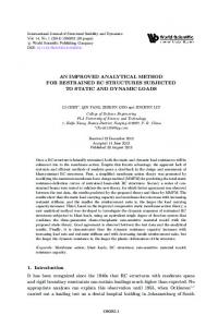
Design for Testability (DFT) has two main aspects, controllability and observability; the control and observation of a circuit are central to implementing its test procedures. We base our method on pseudorandom BIST where the test patterns are generated using Test Pattern Generation Registers (TPGRs), based on autonomous Linear Feedback Shift Register (LFSR) design. The test responses are evaluated using Multiple Input Signature Registers (MISR) [2]. We determine the fault coverage using logic level fault simulation and select the test length (number of test patterns) so as to achieve an acceptable level of fault coverage. One of the di�culties in implementing BIST techniques is the register self-adjacency problem. A register is selfadjacent if an output of that register feeds through combinational logic and back into itself. This situation is depicted in Figure 1(a). In this circuit, a Built-In Logic Block Observer (BILBO) is a register that, in addition to its normal operation mode, operates during test mode as an MISR or as a TPGR [9]. However, it is not possible to assign the output register as both a pattern generator and a signature analyzer, at the same time [7]. This problem can be recti ed using a concurrent built-in logic-block observation (CBILBO) register [2] which can operate simultaneously as an MISR and a TPGR. The disadvantage of the CBILBO is that it is very costly in area (about 1.75 times the size 1 Test overhead refers here to the additional area required to convert normal registers to test, i.e. BIST registers.
TPGR
TPGR
TPGR
TPGR
T=2
ALU
ALU
*
*
m0 +
MISR
Normal
*
a0
(b)
*
m2
m3
Level 2
a0
m2
m3
ALU
...
T=4
Normal
MISR
TPGR T=5
(a)
m1
m1
T=3
BILBO
m0
Level 1 T=1
+ a1 a2 a3
Level 3
a1
Level 4
a2
Level 5
a3
+ +
(c)
Figure 1: (a) Non-Observable ALU due to Self-Adjacency, (b) Extended Testable Functional Block, (c) Self Testable ALU with Self-Adjacent register of a BILBO [11]) and induces more delay during normal operation mode.
2.2 Improved Model for Synthesis with Testability
We base our allocation model on the notion of structural testability at the RT level. The key element of structural testability is the Testable Functional Block (TFB) that we introduced in [17]. The DFG operations are mapped to the ALU of the TFB, while the variables are mapped to the register at the TFB output. The disadvantage of this model is the inability to map operations whose variables life spans overlap to the same TFB; thus, the nal design may use more TFBs than necessary. We now introduce a new improved model for structural testability based on the notion of Extended Testable Functional Blocks (XTFBs), shown in Figure 1(b). An XTFB consists of an ALU and a set of input and output registers. The two registers at the input ports are con gured as TPGRs during test mode. The output port of an XTFB is connected to a set of registers, one of which is con gured as an MISR in test mode. The number of registers at the XTFB output port is optimized during the synthesis process. Although a basic XTFB contains only three BIST registers, namely two TPGRs and one MISR, it should be noted that these BIST registers may be shared by other XTFBs in the datapath. This means that some of these registers may have to be con gured as BILBO registers. Furthermore, some other non-BIST registers at the XTFB output port may have to be con gured as TPGRs only if they control the input port of other XTFBs. The main advantage of the model is that it avoids the dislocation of variable instances from their corresponding operations, keeping them close together during the entire allocation process. This proximity is preserved topologically in the generated data path and it contributes to its structural testability. Con icting variables are mapped to di�erent registers at the output layer of the XTFB. The resulting datapath is guaranteed to be self-testable by construction. Another advantage of our method is its ability to control the sequential depth in the circuit, which we de ne informally as the maximum depth from a controllable to an observable register for a given module.2 Since we always observe the faults at the output port of the ALU, we guarantee a sequential depth of one from the TPGRs to the MISR. However, this depth can be relaxed by the system, or interactively by the designer, using the notion of functional bypassing to perform design and test tradeo�s (sections 4 and 5). 2 Note that this de nition is di�erent from the one in [12, 3] who are not using the BIST methodology.
(a)
(b)
Figure 2: Biquad: (a) DFG, (b) Module Allocation graph (dotted edges correspond to incompatibilities due to library considerations).
3 Testable Datapath Allocation
Our testable datapath allocation starts with a scheduled DFG, generated by any scheduling method reported in the literature. Several key elements characterize our allocation technique: 1) A levelized compatibility graph; 2) a technology library of components; 3) a cost function. In what follows, we describe our method in reference to the simple biquad lter DFG, shown in Figure 2(a).
3.1 Requirement Analysis
Based on our model, two XTFBs are compatible if there is no resource con ict between the operations of the DFG nodes; that is, the nodes are assigned to di�erent time steps in the schedule. However, in addition to the above restriction, we impose two further merging constraints expressed in the following two rules: Rule 1: Do not merge XTFBs if such merging will result in a module which does not exist in the technology library. For example, if the resulting ALU has an operation set such as f+,*,/g which is not in the library, such merging can not take place from the technology library standpoint. Rule 2: Allow self-adjacent registers only if the resulting structure is testable. We do not generate designs such as the ones depicted in Fig. 1(a), while designs as in Fig. 1(c) are testable and thus acceptable. Rule 2 in our model is responsible for the structural testability of our RTL datapath designs.
3.2 System Library
Minimizing the number of components is not su�cient to guarantee a good design since some components may be more expensive than others under a given technology. We use a technology library as an input to our allocation method. The technology library provides information about the layout area of every individual component (width height and break points) along with the delay propagation. The library components, based on an NCR [15] library, are parametrized by their bit length and some may come in di�erent implementation styles, for example, a slow but area e�cient multiplier versus a fast but area expensive multiplier. Furthermore, each component is associated with a set of test metrics which we obtained by fault simulation. These include the fault coverage of individual ALUs along with the module randomness and transparency, detailed in [4].
3.3 Module Allocation Graph
In order to illustrate the compatibility relations among the DFG nodes, we use a special graph, the module allocation
graph (MAG). This is a levelized directed acyclic graph with nodes and levels corresponding to the ones of the scheduled DFG, respectively. An edge from node A to node B of the MAG indicates that these nodes are compatible; however, node A is scheduled before node B . A given path in the MAG corresponds to a list of XTFBs that can share resources. The motivation for the MAG is twofold. First, by having directed edges, a top-bottom optimization process is possible by considering two levels at a time, pruning the number of paths in the MAG. Second, we associate a local cost (gain) function with every path in the MAG. The cost function guides the algorithm in order to select the best merging possibility at every iteration. The MAG is technology dependent and driven by the system library (Rule 1). Thus, for di�erent libraries, we have di�erent MAGs, and consequently di�erent bindings. The construction of the MAG is quite simple: we assign each node in the MAG to the level at which it was scheduled. We add directed edges between the compatible nodes using a top-bottom fashion by considering two levels at a time, k and k + 1. The reason, as stated above, is to prune the number of paths in the MAG and thus reduce the number of edges in the graph. For example, in Figure 2(b), path m0 a1 is redundant since it is covered by path m0 a0 a1. Edges are added to the MAG as long as they do not cause resource con icts. The module allocation graph for the DFG in Figure 2(a) is shown in Figure 2(b) with dotted edges corresponding to incompatibilities due to library considerations.
3.4 Resources Allocation with Testability Consideration
The ultimate goal of the allocation phase is to optimize the cost of the datapath. We accomplish this by merging operations, variables and interconnects, simultaneously. Thus, we construct an initial datapath structure which corresponds to an initial design point. Guided by local cost functions, we improve the design through incremental merging of XTFBs. The local cost functions are associated with every path in the MAG. We de ne the local cost gain of the datapath resulting from merging XTFBs A and B into a third XTFB C as follows: glocal (C ) = gALU + gMux + gReg where gALU ; gMux ; gReg are described shortly in sections 3.4.1, 3.4.2, and 3.4.3. We de ne next the local cost function f associated with a directed edge from A to B in the MAG as: f = glocal (x) + glocal (y) , glocal where x and y are all the nodes connected to A and B , respectively, and glocal is the local cost function associated with merging A and B: The optimization algorithm starts with the nodes in the rst two levels of the MAG and nds the level with the fewest outgoing edges. Obviously, at this level, the nodes with the fewest number of outgoing edges are more restricted than the others. Among these restricted nodes, we choose the nodes with a minimum cost f . The local gain functions glocal can be used to break any ties. After exhausting all the nodes at the level under consideration, we proceed to the following level and update the local cost functions so as to re ect the new structure in the datapath. We repeat this process until all nodes in the MAG have been processed.
P
P
3.4.1 Module Allocation
Every time we merge two ALUs we are reducing the data path cost by the cost of one ALU. Assuming that the combined operation set, ALU 1 [ ALU 2, already exists in the library, we de ne the local cost gain function as:
gALU = Cost(ALU1 ) + Cost(ALU2 ) - Cost(ALU1 [ALU2 )
3.4.2 Mux Allocation
When mapping a commutative operation to an XTFB, there exist two possible con gurations to assign the input ports to the XTFB, left or right mux. For non-commutative operations such as subtraction, the con guration is unique. When considering two XTFBs for merging, we assign the non-commutative operations to the multiplexers at the input ports of the resulting XTFB rst. The remaining assignment is done so as to reduce the number of multiplexer inputs, right or left, through incremental register alignment. If Cost(MUX1) and Cost(MUX2 ) are the multiplexer cost of the original XTFBs, and Cost(MUX ) is the multiplexer cost, then the local cost gain function is de ned as: gMux = Cost(MUX1 ) + Cost(MUX2 ) , Cost(MUX )
3.4.3 Registers Allocation
The register cost gain function estimates the registers cost resulting from merging two XTFBs. The idea is to simply estimate the cost of registers at the output port of the XTFB. We apply locally the Left Edge Algorithm [10] incrementally at the output ports of the resulting XTFB. The restriction is that we do not merge registers that may create some type of self-adjacent registers (Rule 2). Thus, we guarantee the datapath self-testability. The Left-Edge running time is very fast since we are looking at a small list of registers corresponding to only two XTFBs at a time. The register cost function chooses controllable registers (TPGRs) at the resulting XTFB input ports and an observable register (MISR) at the output port. Let n be the number of registers at the output port of the XTFB (Figure 1(b)), and let l be the number of TPGRs. Then, we estimate the cost of registers by: Costreg = Obs Cost + l � TPGR Cost + (n , l , 1) � Normal Cost where Obs Cost is the cost of either an MISR or a BILBO, depending on whether the register needs to control another port in the datapath. Merging two XTFB sets implies merging their output registers as well. We apply the Left Edge Algorithm to the register sets of both XTFBs. If Costreg1 and Costreg2 are the register cost of the two initial XTFBs, and Costreg is the register cost of the resulting one, then the local register cost function is de ned as: gReg = Costreg1 + Costreg2 , Costreg
4 Test Point Selection
Our allocation method guarantees self-testability while keeping the controllable and the observable registers \close" to their individual modules and resulting in a sequential depth of one. To reduce further the test overhead, we perform test point (register) selection while keeping the fault coverage at an acceptable level. The selection is done in two phases. In the initial phase, described shortly, some TPGRs which are not necessary to test the datapath ALUs are eliminated. In the second phase, illustrated by an example in section 5, the system provides the ability to interactively remove/inject BIST registers to explore the design cost, test overhead and fault coverage. As a result of both reduction phases, the datapath area decreases signi cantly. Let n be the number of ALUs in the data path. Let m = 2n be the number of distinct input ports, assuming that every ALU has a Left and Right input port. Let l be the number of registers connected to the m input ports. The test point selection problem then reduces to one of covering every ALU port with a TPGR. However, we do not cover two input ports of an ALU with a single register to avoid adverse fault coverage e�ects (Equation 3). Formally:
Constraints:
X Lefti;j � Xi � 1
j = 1; 2; :::m
(1)
X Righti;j � Xi � 1
j = 1; 2; :::m
(2)
l
i=1 l
i=1
Xl (Righti;j � Lefti;j ) � Xi = 0 i=1
Where
n Lefti;j = 10 n1
Righti;j =
j = 1; 2; :::m (3)
Xi = 0 or 1
(4)
if Reg i covers left port j otherwise if Reg i covers right port j 0 otherwise
Cost function to minimize C=
Xl Xj j=1
(5)
We note that an ILP solution to the above problem is very e�cient and very fast due to the small size of the problem. For our running example of Figure 2(a), the initial phase reduced the number of TPGRs by 6, a reduction of 61.53% of the original number of controllable registers.
5 Test Tradeo�s Illustration Using an Example
The test point selection described above reduces the number of TPGRs in the datapath. However, we can further reduce the number of BIST registers (TPGRS and MISRs) using the test metrics introduced by [4]. The idea is to remove an observable register at the output port of a XTFB if the faults can be sensitized through intermediate modules [4]. Of course, this will increase the sequential depth in the circuit. To illustrate our tradeo� scheme, we use the TRIGO example which computes the Taylor series for the trigonometric functions sin(t=T ) and cos(t=T ). All the operations for this example exist in our library (f+g,f*g,f/g). The test hardware overhead was signi cantly reduced (by 17.96 %) after applying our test point selection. We have experimented with the fault coverage of several design styles for the trigo example versus the number of test patterns as shown in Figure 3. We notice that there is a measurable di�erence in fault coverage quality between the BILBO and the test point selection option, in favor of the BILBO. This di�erence is about 2% but it should be measured against the area increase required by the BILBO designs when making tradeo� decisions. We also note another interesting tradeo� measure that exists between test area overhead and test time or fault coverage. To be speci c, our tradeo� scheme has the capability to \inject" observable points (MISRs) during the design process for the bene t of increasing the fault coverage (or reducing the number of test patterns). Thus, we can generate designs between the BILBO and the test point selection options by performing tradeo�s between test area overhead and fault coverage. By injecting an observable register we can \break" a chain in the circuit, used to bypass test patterns from a controllable point to an observable point. Breaking such chains improves the fault coverage of the circuit at the expense
of increasing the circuit overhead; however, this increase is not very large. These tradeo�s are depicted in Figure 3 which illustrates three fault coverage/test pattern curves corresponding to one, two and three test registers injected. The data points in each curve were derived by injecting a test register from one data point to the next one. Going back to our running example (Figure 2(a)), we have the following comments: The tradeo� scheme reduced the number of observable points by 2. The rst design, based on no test point selection, has the highest fault coverage at the expense of larger area. The second and third designs present a good tradeo� or balance between area and test quality (fault coverage).
6 Results
We implemented the improved allocation and tradeo� scheme on a Sun SPARCstation IPC. The method is very fast and all reported results are produced in at most 12 CPU seconds (wave lter) including scheduling time. We validate our methods using two sets of data. In the rst set we use two examples, a di�erential equation from HAL [18] and an example from FACET [19]. Results are shown in Table 2 and Table 3, respectively. We compare with [11, 16, 19, 18] based on RALLOC [11] cost model. We note that the designs generated by [16, 18, 19] were modi ed by Avra [11] using CBILBOs in order to make them testable. As the results clearly show, the designs generated by our method, while fully testable, have a better cost. The data path cost in this case was de ned [11] as: Cost = 20 � BILBOs + 35 � CBILBOS + MuxIn + Control Signals + Interconnect: We account for two more factors in the above cost formula, the cost of TPGR's and MISR's de ned respectively as: 14 � TPGR + 16 � MISR. These cost factors are dependent upon the technology and implementation used. The second set of data consists of two relatively large benchmark examples, the fth order elliptical wave lter and the AR lter. For the wave lter, rst introduced by [18], we derive four testable designs based on four di�erent schedules, i.e. 17, 19, 21 and 28 time steps. We assume multicyle operations in case of the multiplication while we assume additions take just one cycle. We show the detailed results for this example in terms of components, number and types of test registers, and the overall area of the datapath in Table 4. Table 1 shows the overhead using BILBO designs, and the overhead after applying our tradeo� scheme. The overhead was computed with respect to the overall area of the datapath which includes the area of ALUs, registers (normal and test registers) and multiplexers. In the case of 17 time steps, we notice a substantial overhead reduction, from 23.22 % to 2.18 %. The sequential depth was one in the case of BILBO option as well after the initial selection, while it increased to two after the nal selection. The fault coverage versus the number of random patterns is shown in Fig. 4.
Design example
AR Filter, T = 8 AR Filter, T = 10 Wave Filter, T = 17 Wave Filter, T = 19 Wave Filter, T = 21 Wave Filter, T = 28
Initial Final Overhead Overhead 20.21 % 25.23 % 22.13 % 23.22 % 27.88 % 44.90 %
5.63 % 6.08 % 3.94 % 2.18 % 6.74 % 9.26 %
Table 1: Test overhead before and after tradeo�s
[1] M. Abadir, M. Breuer, \A Knowledge-Based System for Designing Testable VLSI Chips," IEEE Design & Test, Aug. 1985. [2] M. Abramovici, M. Breuer, A. Friedman, Digital Systems Testing and Testable Designs, Computer Science Press, 1990. [3] K. Cheng, V. Agrawal,"Synthesis of Testable Finite State Machines," ISCAS-90, 1990. [4] S. Chiu, C. Papachristou, \A DFT Scheme with Applications to Data Path Synthesis," DAC-91, 1991. [5] G. De Micheli et al., \The Olympus Synthesis System for Digital Design," Tech. Report, Stanford University. [6] C. Gebotys, M. Elmasri, \VLSI Design Synthesis with Testability," DAC-88, 1988. [7] C.L. Hudson, G. Peterson, \Parallel Self-Test With Pseudo-Random Test Patterns," ITC-87, 1987. [8] R. Jain, K. Kukukcakar, M. Mlinar, A. Parker, \Experience with The Adam Synthesis System," DAC-89, 1989. [9] B. Koenemann, J. Mucha, G. Zwieho�, \Built-In Logic Block Observation Techniques," ITC-79, 1979. [10] F. Kurdahi, A. Parker, \REAL: A Program for Register Allocation," DAC-87, 1987. [11] LaNae Avra, \Allocation and Assignment in HighLevel Synthesis for Self-Testable Data Paths," ITC-91, 1991. [12] T. Lee, W. Wolf, N. Jha, J. Acken, \Behavioral Synthesis for Easy Testability in Data Path Allocation," ICCD-92, 1992. [13] J. Lis, D. Gajski, \Synthesis from VHDL," ICCD-88, 1988. [14] A. Majumdar, K. Saluja, R. Jain, \Incorporating Testability Considerations in High-Level Synthesis," FTCS-92, 1992. [15] The NCR ASIC Data Book, 1989. [16] B. Pangrle, \Splicer: A Heuristic Approach to Connectivity Binding," DAC-88, 1988. [17] C. Papachristou, S. Chiu, H. Harmanani, \A Data Path Synthesis Method for Self-Testable Designs," DAC-91, 1991. [18] P. Paulin, J. Knight, \Force-Directed Scheduling for the Behavioral Synthesis of ASIC's", IEEE Trans. CAD, Vol 8, 1989. [19] C. Tseng, D. P. Siewiorek, \Automated Synthesis of Data Paths in Digital Systems," IEEE Trans. CAD, 1986. [20] H. Harmanani, C. Papachristou, S. Chiu and M. Nourani, \SYNTEST: An Environment for SystemLevel Design for Test," EURO-DAC 92, Sept. 1992.
Bilbo Bist Select One (*+) Chain Two (*+) Chain Three (*+) Chain
60000
Number of Test patterns
50000
40000
30000
20000
10000
0 92
93
94
95 Fault Coverage (%)
96
97
98
Figure 3: Fault coverage for the trigo example after injecting one, two, and three additional test points
25000 Time Step 17 Time Step 19 Time Step 21 20000 Number of Test patterns
References
70000
15000
10000
5000
93.5
94
94.5
95
95.5 96 Fault Coverage (%)
96.5
97
97.5
98
Figure 4: Fault coverage for the wave lter example
20000 Time Step 8 Time Step 10
18000 16000 Number of Test patterns
The AR Filter was used initially by [8]. We derived two schedules using time steps 8 and 10 assuming that all operations execute in one cycle. We show detailed results for this example in Table 5. Table 1 illustrates the overhead using BILBO designs, then the overhead after applying our tradeo�s. We note that the sequential depth was one in case of the BILBO option and initial selection, but increased to two after the nal selection. The fault coverage for this example versus the number of patterns is shown in Fig. 5. To conclude, we have integrated all the software of our presented method into SYNTEST, a high level synthesis for testability system that we have developed at CWRU, whose details are reported in [20].
14000 12000 10000 8000 6000 4000 2000 93
94
95 96 Fault Coverage (%)
97
Figure 5: Fault coverage for the AR lter example
98
System
ALUs
Splicer HAL RALLOC Ours
(*)(*)(+)(-)(>) (*)(*)(+)(-)(>) (*)(*) (-) (+) (+*)(*->) (*+)
BILBO CBILBO TPGR MISR Mux Inter- Control Cost In Connect Signals 1 1 4 0
5 4 1 0
0 0 0 4
0 0 0 1
17 19 22 15
34 35 38 28
23 24 27 21
269 238 202 136
Table 2: Designs Comparisons for the HAL Di�erential Equation example
System
ALUs
Facet Splicer HAL RALLOC Ours
(/)(-&+)(*j+) (/)(-&+)(*j+) (/)(-&+) (*j+) (+/j)(-&+) (*+) (+/)(-&+) (*j+)
BILBO CBILBO TPGR MISR Mux Inter- Control Cost In Connect Signals 3 4 4 4 0
5 3 1 1 0
0 0 0 0 3
0 0 0 0 1
15 11 13 16 10
31 26 23 29 21
23 18 17 21 16
Table 3: Designs Comparison for the FACET Example
C Step 17
19 21 28
Mode Normal BILBO Initial Selection Final Selection Normal BILBO Initial Selection Final Selection Normal BILBO Initial Selection Final Selection Normal BILBO Initial Selection Final Selection
ALUs
3 (*), 3 (+) 3 (*), 3 (+) 3 (*), 3 (+) 3 (*), 3 (+) 2 (*), 2 (+) 2 (*), 2 (+) 2 (*), 2 (+) 2 (*), 2 (+) (*), 2 (+) (*), 2 (+) (*), 2 (+) (*), 2 (+) (*), (+) (*), (+) (*), (+) (*), (+)
BILBO TPGR MISR # Reg Mux In Area (�2 ) 0 6 2 2 0 4 1 1 0 3 1 1 0 5 0 0
0 3 3 3 0 5 2 2 0 3 2 2 0 2 2 2
0 0 4 2 0 0 3 1 0 0 4 2 0 0 2 2
15 15 15 15 14 14 14 14 11 11 11 11 17 17 17 17
32 32 32 32 29 29 29 29 31 31 31 31 32 32 32 32
101,500 127,480 110,964 105,500 76,760 98,100 83,904 78,440 65,260 87,668 72,396 69,664 60,246 87,302 65,830 65,830
Table 4: Results Summary from the wave lter
C Step 8
10
Mode Normal BILBO Initial Selection Final Selection Normal BILBO Initial Selection Final Selection
ALUs
3 (*), 3 (+) 3 (*), 3 (+) 3 (*), 3 (+) 3 (*), 3 (+) 2 (*), 2 (+) 2 (*), 2 (+) 2 (*), 2 (+) 2 (*), 2 (+)
BILBO TPGR MISR # Reg Mux In Area (�2 ) 0 6 2 0 0 4 2 1
0 8 2 4 0 5 1 2
0 0 4 4 0 0 2 2
16 16 16 16 14 14 14 14
Table 5: Results Summary from the AR Filter
31 31 31 31 28 28 28 28
103,292 125,568 114,356 109,116 70,540 91,152 77,564 74,832
304 240 168 181 105