gyroscopes are fabricated in parallel with the folded structure on the same substrate, and are electrically and mechanically interfaced through integrated flexible ...
Chip-Scale IMU Using Folded-MEMS Approach Sergei A. Zotov, Montgomery C. Rivers, Alexander A. Trusov, Andrei M. Shkel MicroSystems Lab, Department of Mechanical and Aerospace Engineering University of California at Irvine, Irvine, CA, USA Email: {szotov, mrivers, atrusov, ashkel}@uci.edu Abstract—This paper reports a new approach to design and fabrication of chip-level inertial measurement units (IMUs). The folded-chip method utilizes a 3-D foldable silicon-oninsulator (SOI) backbone suitable for high-aspect ratio sensor fabrication. Assembly is done on the wafer level forming a compact rigid 6-axis system of sensors. Accelerometers and gyroscopes are fabricated in parallel with the folded structure on the same substrate, and are electrically and mechanically interfaced through integrated flexible polyimide film hinges and interlocking silicon latches. To demonstrate feasibility of the approach, folded IMUs are fabricated containing resonant capacitive accelerometers and gyroscopes. The value of the scale factor of the accelerometers is tunable over a range from 1.75 Hz/g to 3.7 Hz/g. Driving the gyroscope on the pyramid sidewall with 1.5 kHz operational frequency, the rotation rate is characterized in air to demonstrate operation with a scale factor of 0.43 mV/(deg/sec). Structural rigidity was verified by subjecting the IMU to oscillations from 50 Hz – 3.5 kHz over an amplitude range of 5 – 25 g. The results confirm feasibility of the proposed folded MEMS IMU approach, and may enable new integrated architectures for other multi-axis dynamic sensors, such as 3-D microphones, hydrophones, and ultrasonic transducers.
I.
INTRODUCTION
Inertial sensing is used in a wide variety of applications including navigation, defense, exploration, automotive and robotics [1]. For complete detection of motion, rotation and acceleration must be measured along three axes, creating a 6axis Inertial Measurement Unit (IMU). Due to the increasing number of applications that require position and navigation information, miniaturization of IMUs is essential. One main challenge in development of a compact IMU is combining multiple high-performance sensors capable of detecting motion along independent sensitive axes with minimal crossaxis sensitivity and mechanical and electrical coupling. Current methods for creating miniature IMUs typically rely on either assemblies of separate printed circuit board (PCB) modules containing individual single-axis sensors [2], or consist of multi-axis sensors which utilize multiple degrees of freedom of a single proof mass [3,4]. While the PCB level approach allows for the use of optimized, high-performance single-axis sensors, its further miniaturization is limited. In contrast, integration of multi-axis sensors on the same substrate provides small form factor but suffers from more complex fabrication, compromises in sensor design and
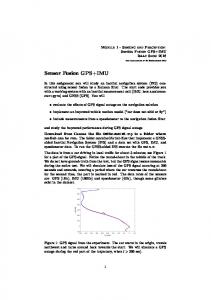
Electrical Interconnects
Gyroscope
Interlocking Latches
Accelerometer Gyroscope
8m m
10
Accelerometer
m
m
Flexible Hinges
Figure 1. Assembled IMU cube and pyramid with operational sensors.
performance, and crosstalk between the sensitive axes. This leads to a tradeoff between size and performance, leaving no clear path toward a high-performance chip-level IMU utilizing existing techniques. II.
APPROACH
To overcome the challenges faced by existing techniques used for creating compact IMUs, a novel approach has been explored using a folded-chip structure with inertial sensors located on each surface. Independent sensors are fabricated on a foldable backbone that is assembled to provide a package volume less than 1 cm3. Flexible hinges allow the dies to fold together, and interlocking latches are provided to lock the panels into place. Electrical interconnects travel from each sidewall to the base of the structure to allow for flip-chip packaging. With this method, single-axis sensors are implemented in a 3-D spatial configuration along independent axes to create a compact high-performance IMU with minimal cross-talk and cross-axis sensitivity [5]. Fig. 1 shows a fabricated IMU cube and pyramid structure with operational inertial sensors. Several design challenges are involved with developing an IMU with the proposed approach such as structural rigidity, durability, sensor alignment, and packaging. Design features to accommodate desired functionality have been included to minimize each issue, Fig. 2. An interlocking latch design is used along each edge that provides rigidity and alignment of the folded structure. Compliant hinges are provided to allow for folding the sidewalls into place. Significant flexibility is required for assembly, as well as durability, the capability of carrying electrical signals, and adhesion to the silicon and metal interconnects. Polyimide has many of these
This work was supported by the DARPA Microsystems Technology Office under Grant No. W31P4Q-08-1-0008.
978-1-4244-8168-2/10/$26.00 ©2010 IEEE
1043
IEEE SENSORS 2010 Conference
Interlocking Latches
Flat Structure
Hinge Fingers Minimize lateral movement between sidewalls
Metal Traces
Polyimide Weldable Edges Hinge Gap
Sensors Allows for bend in polyimide
Assembled IMU
Electrical Interconnects
Figure 3. Approach for fabrication of folded IMU structures.
Figure 2. Design features of a folded IMU cube.
characteristics, and is identified as an optimal material for this purpose. Hinge fingers are included at the base of each sidewall to reduce lateral movement of one sidewall with respect to another. Gap width of the hinges determines the bending radius and stress induced on the polyimide. The design shown allows for a 500 µm radius, which creates minimal stress in the polyimide. For packaging purposes, electrical interconnects terminate on the bottom of the cube enabling flip-chip bonding. Traces are designed to minimize impedance by optimizing the width, thickness, and pitch. Fabrication of the folded IMU structures involves creating the sensors, patterning a flexible material around the sensors to function as hinges, and deposition of metal interconnects on top of the hinge material, Fig. 3. To release the foldable structures, the backside of the wafer is etched through using deep reactive ion etching (DRIE). Assembly is done by folding the panels together into a 3-D configuration. For an IMU, an ideal structure is that of a cube with individual sensors on each sidewall, however pyramidal structures are also being explored. Structurally, a pyramid is more rigid than a cube, and therefore provides a preferred platform for inertial sensing. Other types of structures also can be created for various applications using the same fabrication process developed for the cube and pyramid designs. III.
FABRICATION
A fabrication process has been developed for manufacturing folded IMU structures. Sensors are made using Silicon-On-Insulator (SOI) technology, enabling high-aspect ratio devices for excellent overall performance. By utilizing SOI fabrication, there is great flexibility in the type of designs used for both accelerometers and gyroscopes. Therefore the folded MEMS approach is very modular and can be used for many inertial measurement applications.
The polyimide used in this process is HD-4110, which has a nominal thickness of 20 μm after curing, and contains a negative photosensitive resist that allows for direct lithographic patterning. One concern is the ability to maintain adhesion of polyimide to silicon and metal. Bulk polyimide shows resilience to most solvents and a wide variety of acids and bases. However, the adhesion layer is more susceptible to damage, and can cause delamination. For optimal adhesion properties, the recipe parameters in Table 1 were used for polyimide deposition. Metal is deposited on top of the cured polyimide and patterned using lift-off. The photoresist used is AZ nLoF 2035, which is specifically designed for lift-off processes. Using electron beam evaporation, a 500 Å layer of chrome is first applied for adhesion, followed by 5000 Å of gold. Impedance of the traces is minimal with this procedure, creating interconnects with a maximum measured resistance of 3.8 Ω, which is acceptable for the folded IMU. Sensors are defined using a photoresist mask, and etching is performed with DRIE for 50 μm to reach the buried oxide, as shown in Fig. 4b. For backside processing, a blanket coating of photoresist, as well as dicing tape is used to protect the existing front-side features from physical damage. After processing, the sample is soaked in acetone which removes the tape and photoresist. Backside etching then ensues by patterning a double-layer of AZ P4620 photoresist. DRIE is used to etch the silicon layers; however a different technique must be employed to etch the buried oxide layer. For the process step shown in Fig. 4c, buffered oxide etch (BOE) is used because of its compatibility with the photoresist mask.
Processing is done utilizing the fabrication steps shown in Fig. 4. Initially, polyimide is deposited and patterned onto the device layer (top) of the substrate (Fig. 4a). For durability purposes, it is desired to have a thick polyimide that can withstand dynamic loading over an extended period of time.
1044
TABLE I.
POLYIMIDE DEPOSITION RECIPE PARAMETERS Recipe Parameter
Specification
Spin Rate
1500 rpm
Soft Bake
12 min @ 120°C 2
Exposure Time (@ 10 mW/cm ) Post Exposure Bake (PEB)
60 sec 5 min @ 120°C
Metal Polyimide
20
Scale Factor (Hz/g)
SOI wafer a. Metal and polyimide deposition and patterning
Natural Frequency 1120 Hz Proof Mass 0.75e-6 kg Nominal Capacitance 1.2 pF
15 10 1.75 Hz/g
4.08 Hz/g
5
b. Definition of sensors using photolithography and DRIE 0
10
40 30 Applied DC Voltage (V)
50
60
Figure 5. Accelerometer used on the folded IMU (upper left) and the corresponding tunable scale factor for 0-60 V bias.
c. Backside through etch using DRIE
V. Sensor d. Release of SOI sensors using HF etching
EXPERIMENTAL RESULTS
This section reports experimental characterization of accelerometers and gyroscopes on the folded structures. The devices were fabricated utilizing the fabrication sequence shown in Fig. 4.
Figure 4. Process for creating folded structures with in-situ fabrication of sensors, flexible hinges, and metal interconnects.
After the backside etch is complete, the foldable IMU structures are removed from the wafer and cleaned of any residue. The underlying oxide is etched with hydrofluoric acid (HF) or BOE to release the inertial sensors and finish fabrication (Fig. 4d). Assembly and packaging of the folded structures are then done to create a complete chip-scale IMU. Both cubic and pyramidic IMUs have been fabricated with operational inertial sensors and a footprint of less than 1 cm2. IV.
20
STRUCTURAL RIGIDITY
One major concern with the IMUs fabricated using the approach is rigidity of the enveloping structure and stability of inertial axes orientation. After initial calibration, misalignments from impact or high acceleration loads will cause bias errors in the output signals. To initially test structural rigidity, vibration testing has been conducted on samples using an electrostatic shaker unit. Oscillations were induced from 50 Hz – 3.5 kHz over a range of 5 – 25 g, resulting in no damage to the structure. While this shows that the interlocking latches provide rigidity, more stringent testing is required for many applications. For high shock and acceleration loads, it is desired to bond the sidewalls together to enhance structural rigidity. Silicon-to-silicon welding is being explored to provide a method for increasing maximum rigidity by creating permanent homogeneous joints along the sidewall edges. Advantages of this approach are the lack of variation in material thermal properties, as well as overall rigidity of the folded structure. Resistive welding is a common technique used for bulk materials, using a DC current to melt the weld joint. Feasibility of resistive welding of silicon has been successfully demonstrated on a 50 µm SOI device. To apply this technique to the folded structure, a similar process is being developed for welding of the interlocking latches to provide a stable, rigid platform for inertial sensing.
A. Characterization of Accelerometer The design of the accelerometer consists of a proof mass suspended by folded springs to fixed anchors, parallel plate sense electrodes, and electrostatic comb drives. For the folded IMU, resonant detection of acceleration is chosen to provide high dynamic range and direct digital output [1]. This method is also resilient to noise induced by parasitic capacitance because it utilizes tracking of a resonance peak at a much higher gain than the noise level. Acceleration is detected by monitoring the changes in resonant frequency due to electrostatic tuning while undergoing inertial input. For small deflections of the proof mass and small amplitude of oscillation, the natural frequency can be expressed as
ωN =
k ξ AV 2 − m m(d 0 − ma / k ) 3
,
(1)
where m is the proof mass, a is the applied acceleration, k is the spring stiffness, V is the bias voltage, d0 is the initial gap in the sense plates, and A is the overall area of capacitors [6]. From the equation it is seen that the natural frequency is dependent on the change in applied acceleration. An additional advantage of this detection method is that the sensitivity of the device can be actively tuned during operation. Using one set of parallel plates on the device, a DC voltage is applied to displace the proof mass. This displacement modifies the initial capacitive gap, d0, and thus the overall sensitivity is changed. Fig. 5 shows a plot of the scale factor calculated with (1) over a range of 0-60 VDC bias voltage with the parameters of the accelerometer. Acceleration is tested is by measuring response to gravity at different angles on a tilt stage. Vertical angles can be applied in increments of five degrees to apply a range of acceleration from 0-1 g. At each position, the resonant
1045
3.5
Proof Mass
3
Drive and Sense Electrodes
Drive and Sense Electrodes 50
SF 3.7 Hz/g
Output (mV)
-3
Df/f ( 10 )
2.5 2
1.5
SF 0.43 mV/( /s)
0
SF 1.8 Hz/g
1
-50
0.5
0
Proof Mass
100
Measured data (20V) Measured data (30V) 0.4 0.6 Acceleration (g)
0.2
Measured data Linear fit
Linear fit Linear fit 0.8
-100 1
-250 -200 -150 -100
Figure 6. Measured acceleration response of a resonant accelerometer on a folded IMU pyramid showing normalized shift in resonant frequency.
frequency is measured to determine the shift caused by acceleration input, and the results are plotted in Fig. 6. Using a DC bias voltage of 20 V, the sensitivity is determined to be 1.8 Hz/g. When 30 V bias is used, the scale factor is increased to 3.7 Hz/g. Comparing these values to the plot in Fig. 5, the calculated sensitivities are 1.75 Hz/g and 4.08 Hz/g, respectively. Because measured and calculated values agree well, this indicates that that (1) is an accurate analytical model for determining the scale factor of resonant accelerometers. B. Characterization of Gyroscope Angular rate performance of the gyroscope fabricated on the sidewall of a pyramid is experimentally characterized in air. To test rotation response, the pyramid structure is mounted to a computer controlled Ideal Aerosmith 1291BR rate table. The drive mode of the gyroscope is excited at resonance using a combination of 30 VDC bias and 5 VAC driving signal applied to the anchored drive-mode electrodes. Separation of the useful signal from the feed-through signal is accomplished using electromechanical amplitude modulation (EAM), where a carrier voltage of 3.5 Vrms at 52 kHz is applied to the proof mass resulting in the amplitude modulation of the motional signal. Two demodulations, first at the carrier frequency and then at the drive frequency, are used to extract the motional signal from the total EAM pickup signal. Fig. 7 shows the detected rate response of the gyroscope [7] fabricated on the folded IMU pyramid with a scale factor of 0.43 mV/(deg/sec) over an input range of ±250 deg/s, confirming suitability of the approach. VI.
A new approach for creating a chip-scale IMU has been described using foldable MEMS structures. A wafer-scale fabrication process is illustrated for manufacturing IMUs with SOI sensors, and several challenges have been identified. Cubic and pyramid IMU configurations have been investigated. Rigidity of the structure has been analyzed, showing the micromachined latches to be a feasible method for supporting an inertial platform. Acceleration and rate response on the IMU cubes and pyramids have been tested,
150
200
250
Figure 7. Measured rotation rate response of a gyroscope on a folded IMU pyramid over a range of -250 to 250 deg/s.
indicating that the described process is compatible with fabrication of SOI sensors. The results confirm feasibility of the proposed folded MEMS IMU approach, and may enable new integrated architectures for other multi-axis dynamic sensors, such as 3-D microphones, hydrophones, and ultrasonic transducers. ACKNOWLEDGMENT This work was supported by the Microsystems Technology Office of DARPA contract W31P4Q-08-1-0008. The authors would like to acknowledge University of California, Irvine Integrated Nanosystems Research Facility (INRF) for assistance with the fabrication of prototypes, the Zeiss Center of Excellence for providing the microscopes necessary for SEM imaging, Roger Young at FAST Semiconductor for assistance in packaging, and Igor Prikhodko for discussions on testing. The folded IMU structures were designed and characterized at the MicroSystems Laboratory, University of California, Irvine. REFERENCES [1] [2] [3]
[4]
CONCLUSION
0 -50 50 100 Input Angular Rate (°/s)
[5]
[6]
[7]
1046
Liu, Kai, et al., “The development of micro-gyroscope technology,” Journal of Micromechanics and Microengineering, vol.19, no.11, 2009. W. Geiger, et al., “MEMS IMU for AHRS applications,” Position, Location and Navigation Symposium, 2008, pp.225-231, May 2008. S. Habibi, S.J. Cooper, J.M. Stauffer, B. Dutoit, “Gun hard inertial measurement unit based on MEMS capacitive accelerometer and rate sensor,” PLANS, 2008, pp.232-237, May 2008. M. Meng, Z. Wu, Y. Yu, Y. Ge, Y. Ge, “Design and Characterization of a Six-axis Accelerometer,” IEEE Conference on Robotics and Automation, pp. 2356- 2361, April 2005. M. C. Rivers, A. A. Trusov, S. A. Zotov, A. M. Shkel, “Micro IMU Utilizing Folded Cube Approach,” IMAPS Device Packaging Conference, Mar. 2010. S. Sung, J.G. Lee, T. Kang, J.W. Song, “Development of a tunable resonant accelerometer with self-sustained oscillation loop,” National Aerospace and Electronics Conference, Proceedings of the IEEE, pp.354-361, 2000. M. S. Kranz and G. K. Fedder, “Micromechanical Vibratory Rate Gyroscopes Fabricated in Conventional CMOS,” Symposium Gyro Technology 1997, Stuttgart, Germany, 9/16–17/97, (1997), pp. 3.0–3.8.