IEEE TRANSACTIONS ON CIRCUITS AND SYSTEMS—I: REGULAR PAPERS, VOL. 61, NO. 2, FEBRUARY 2014
443
Synchronous Non-Volatile Logic Gate Design Based on Resistive Switching Memories Weisheng Zhao, Member, IEEE, Mathieu Moreau, Erya Deng, Yue Zhang, Member, IEEE, Jean-Michel Portal, Jacques-Olivier Klein, Member, IEEE, Marc Bocquet, Hassen Aziza, Damien Deleruyelle, Christophe Muller, Damien Querlioz, Member, IEEE, Nesrine Ben Romdhane, Dafiné Ravelosona, and Claude Chappert, Member, IEEE
Abstract—Emerging non-volatile memories (NVM) based on resistive switching mechanism (RS) such as STT-MRAM, OxRRAM and CBRAM etc., are under intense R&D investigation by both academics and industries. They provide high write/read speed, low power and good endurance (e.g., ) beyond mainstream NVMs, which allow them to be embedded directly with logic units for computing purpose. This integration could increase significantly the power/die area efficiency, and then overcome definitively the power/speed bottlenecks of modern VLSIs. This paper presents firstly a theoretical investigation of synchronous NV logic gates based on RS memories (RS-NVL). Special design techniques and strategies are proposed to optimize the structure according to different resistive characteristics of NVMs. To validate this study, we simulated a non-volatile full-adder (NVFA) with two types of NVMs: STT-MRAM and OxRRAM by using CMOS 40 nm design kit and compact models, which includes related physics and experimental parameters. They show interesting power, speed and area gain compared with synchronized CMOS FA while keeping good reliability. Index Terms—Complementary cells, low-power design, non-volatile memory, resistive switching, synchronous logic gate.
I. INTRODUCTION
M
ODERN computing systems suffer from rising power dissipation including both static and dynamic parts [1], [2]. The static power is driven by the high leakage currents, which increase exponentially with the minimization of fabrication node. The dynamic power is induced mainly by the data transfer between memory chip and logic units, which requires more power (i.e., 1 pJ/mm/bit) than the transistor switching (e.g., 1 fJ/bit), and then imposes the speed bottleneck to adapt the current cooling systems [2]. Lots of research, from the device to the system level, is under intense investigation to find a
Manuscript received October 23, 2012; revised February 21, 2013, April 19, 2013; accepted June 10, 2013. Date of publication August 23, 2013; date of current version January 24, 2014. This work was supported in part by the French national projects NANOINNOV SPIN, CNRS-PEPS NVCPU, ANR-DIPMEM, ANR-MARS and European project FP7 MAGWIRE. This paper was recommended by Associate Editor M. Anis. W.S. Zhao, E. Deng, Y. Zhang, J.-O. Klein, D. Querlioz, N. Ben Romdhane, D. Ravelosona and C. Chappert are with are with IEF, Univ. Paris-Sud and UMR8622, CNRS, Orsay 91405, France (e-mail:
[email protected]). M. Moreau, J.-M. Portal, M. Bocquet, H. Aziza, D. Deleruyelle, and C. Muller are with Aix-Marseille University, IM2NP-UMR CNRS 7334, Marseille, France. Color versions of one or more of the figures in this paper are available online at http://ieeexplore.ieee.org. Digital Object Identifier 10.1109/TCSI.2013.2278332
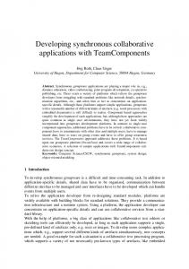
Fig. 1. (a) 2D structure of CMOS logic and memory connection (b) 3D structure of hybrid RS-NVM/CMOS logic, the distance between logic and memory can be greatly reduced. This accelerates the computing speed and economizes the data traffic power.
revolutionary solution to overcome definitively the bottlenecks [3]–[17]. Integrating the resistive switching non-volatile memories (RS-NVMs) such as spin transfer torque magnetic RAM (STT-MRAM) [3], oxide resistive RAM (OxRRAM) [4] and conductive-bridge RAM (CBRAM) [5], is widely considered as a promising approach thanks to their fast write/read speed, low switching/sensing power and good endurance (e.g., ) [6]–[9]. They are classified also to memristor devices [10], [11]. Firstly, their non-volatility allows the system to be powered off completely in “idle” state. This cuts down significantly the static power, particularly for the normally-off electronics such as mobile phones and notebooks [8]. The 3-D integration at the back-end CMOS process of these NVMs shortens greatly the distance between the memory chip and logic units from millimeters to micrometers (see Fig. 1). This lowers the dynamic power dedicated to data transfer and accelerates the access speed compared with conventional systems. Even though these emerging RS-NVMs are derived from different physics, they hold many common features. For instance, they are two-terminal nanoscale devices and their resistances vary to present ‘0’ and ‘1’ NV states. Benefiting from these features, a number of innovative hybrid RS-NVM/CMOS circuit have been designed in the last few years such as NV look-uptable (NV-LUT) [12], NV Flip-Flop (NVFF) [13]–[15] and NV Full Adder (NVFA) [16]–[19]. They show interesting performance in terms of power, area and speed. However there is no general design rule so far for these hybrid circuits and it is difficult to extend them for all types of RS-NVMs. Moreover, most of these circuits suffer from critical limits. For instance, [16]–[18] use magnetic fields or capacitance, which cannot be used in deep submicron ICs. In this context, this paper presents a theoretical design investigation of RS-NVMs based synchronous NV logic gates (RS-NVL). Special techniques and strategies are studied to optimize the circuit area while being compliant with different re-
1549-8328 © 2013 IEEE. Personal use is permitted, but republication/redistribution requires IEEE permission. See http://www.ieee.org/publications_standards/publications/rights/index.html for more information.
444
IEEE TRANSACTIONS ON CIRCUITS AND SYSTEMS—I: REGULAR PAPERS, VOL. 61, NO. 2, FEBRUARY 2014
sistive characteristics of RS-NVMs. The “AND” and “XOR” logic gates are given as examples to illustrate this resistance configuration dependence of RS-NVL design. In order to validate this study, we simulated a NVFA with two types of NVMs: STT-MRAM and OxRRAM by using CMOS 40 nm design kit and compact models [20], [21]. The rest of the paper is organized as follows. In the next section, we introduce briefly two RS-NVM technologies: STTMRAM and OxRRAM. In Section III, the general circuit design of RS-NVL is shown, and its optimization for different RS-NVM is described. Section IV is dedicated to the transient simulation and performance comparison of NVFAs on 40 nm node. Finally, we discuss the implications of our results and conclude in Section V. II. EMERGING RESISTIVE SWITCHING NON-VOLATILE MEMORIES (RS-NVMS) STT-MRAM and OxRRAM are studied as RS-NVMs in the proposed RS-NVL structure. In the following, we introduce briefly these two technologies and their compact models used for electrical and statistical simulation. These compact models rely on physical models and are in good agreement with experimental measurements. A. STT-MRAM Technology Principle and Compact Model MRAM cells integrate a magnetic tunnel junction (MTJ) consisting of a thin insulating barrier (i.e., MgO) separating two ferromagnetic (FM) layers (Fig. 2(a)). Thanks to the tunnel magneto-resistance (TMR) effect [22], its resistance, or , depends on the relative orientation, Parallel (P) or Anti-Parallel (AP), of magnetizations in the two FM layers. STT is a promising switching mechanism that gathers high power efficiency and fast speed [3]. This basic physical mechanism enables profoundly simplifying CMOS circuitry compared with conventional magnetic field switching, as only a bipolar current is required (Fig. 2(b)). MTJ switches as the passing current exceeds a given critical current noted . Recent progress demonstrates that perpendicular magnetic anisotropy (PMA) in CoFeB/MgO structures [23], [24] provides a high-energy barrier to face the thermal instability of in-plane anisotropy. It also presents the advantages of lower threshold current, higher speed operation than in-plane MTJ while keeping a high TMR ratio (e.g., 200%). The experimentally-validated CoFeB/MgO/CoFeB STT-MTJ compact model from [20], taking into account related static, dynamic and stochastic behaviors was used to perform the transient simulation of NVL with CMOS circuits [22]–[24]. Table I shows the critical parameters used in the model. Free layer thickness, oxide barrier thickness and TMR ratio have been used as critical parameters for PVT variation simulation. Thanks to the recent progress on thin film deposition, 1% variation of these parameters can be achieved. This leads to % variation for the electrical characteristics [25]. This model is programmed in spice-compatible Verilog-a language [20] and the following transient simulations were performed on the Spectre simulator of Cadence.
Fig. 2. (a) Vertical structure of an MTJ nanopillar composed of CoFeB (1.3)/ MgO(0.85)/CoFeB(2) thin films. (b) Spin transfer torque switching mechanism: the MTJ state changes from parallel (P) to anti-parallel (AP) as the positive , on the contrast, its state will return as electron flow direction . the negative electron flow direction
TABLE I PARAMETERS AND VARIABLES PRESENT IN THE FITTING FUNCTIONS
B. OxRRAM Technology Principle and Compact Model In its simplest form, an OxRRAM memory element relies on a Metal/Insulator/Metal (MIM) stack (see Fig. 3(a)). The MIM structure is generally composed of metallic electrodes sandwiching an active layer, usually an oxygen-deficient oxide. A large number of resistive switching oxides, like HfO , Ta O , NiO, TiO or Cu O, have been reported in the literature [26], [27]. After an initial electroforming process, the memory element may be switched reversibly between a High Resistance State , and a Low Resistance State . In the case of bipolar switching addressed in this paper, bipolar voltage sweeps, over specific threshold voltage ( and ), are required to switch the memory cell (see Fig. 3(b)). Even if OxRRAM technology is still in its infancy, it is broadly accepted that the field-assisted motion of oxygen
ZHAO et al.: SYNCHRONOUS NON-VOLATILE LOGIC GATE DESIGN
445
Fig. 4. Logic gates composed of PCSA, MOS logic tree and RS-NVMs.
Fig. 3. (a) OxRRAM memory element stack and (b) typical current-voltage characteristic of a bipolar OxRRAM memory device.
TABLE II CELL OPERATION PARAMETERS. POWER SUPPLY IS 1.2 V
vacancies often plays a predominant role in bipolar resistance switching [28]. The proposed OxRRAM modeling approach, deriving from a unipolar model [29], relies on electric field-induced migration of oxygen vacancies within the switching layer. This model enables continuously accounting for both set and reset operations into a single master equation and demonstrates its flexibility to match static (switching voltages, current levels) and dynamic behaviors of the most aggressive component from literature [32]–[34]. Tables II summarizes the cell operation parameters for short programming pulse used for the OxRRAM-based NVFA transient simulations. This model is programmed in GUDM language [21] and the following transient simulations were performed on the Eldo simulator of Mentor Graphics. Even though these RS-NVMs hold the common features, their resistive characteristics are quite different. For STT-MRAM, its low resistance is often some k and the TMR ratio is from 100% to % [22], which limits the high resistance up to k [23]. For OxRRAM, its could be larger than k and its / ratio achieves up a high value [26], [27]. The RS-NVL
Fig. 5. (a) Schematic of Pre-Charge Sense Amplifier (PCSA) (b) Schematic of writing circuit for RS-NVMs.
should be designed carefully to adapt this intrinsic difference of RS-NVMs. III. RESISTIVE SWITCHING NON-VOLATILE LOGIC (RS-NVL) STRUCTURES AND OPTIMIZATIONS A. General Synchronous RS-NVL Structure This general structure or algorithm of synchronous logic gate based on STT-MRAM was initialized in [16] and named “logic-in-memory” architecture. It allows a novel combination between logic unit and memory cell beyond Von-Neumann
446
IEEE TRANSACTIONS ON CIRCUITS AND SYSTEMS—I: REGULAR PAPERS, VOL. 61, NO. 2, FEBRUARY 2014
TABLE III TRUTH TABLE OF THE OPTIMIZED AND LOGIC STRUCTURE-1
TABLE IV RESITANCE CONDITION FOR THE OPTIMIZED STRUCTURE-1 (SEE FIG. 6(C))
Fig. 6. (a) General structure for AND logic gate. (b) One sub-branch RB0 can be deleted from the structure without any impact. (c) The optimized structure 1 for “AND” logic (d) The optimized structure 2 for “AND” logic.
architecture. The data movement distance becomes much shorter, and this promises lower power and faster speed. In this paper, we extend this structure from STT-MRAM to universal RS-NVMs. According to their different resistance characteristics, a detailed theoretical analysis will be introduced for structure optimization. The general structure is mainly composed of three parts: a fast speed dynamical-mode sense amplifier (SA), volatile or fragile logic data and non-volatile or secure analog data as shown in Fig. 4. In order to perform the logic function, a SA is firstly required as the RS-NVM cell with analog data is integrated directly with the logic circuit. This SA should be fast, robust and consume low power to ensure the computing purpose of this structure. Different from the SA for memory chip, it is impossible to embed error correction circuits (ECC) and to share the circuit for multi-cells. Thereby we use here the pre-charge sense amplifier (PCSA) [33], which showed high performance in terms of reliability, power and speed. There is no capacitance in this structure, which allows better minimization in advanced fabrication node than [17]. As shown in Fig. 5(a), a PCSA consists of a pre-charge subcircuit (MP2-3), a discharge sub-circuit (MN2) and a pair of inverters (MN0-1 and MP0-1), which act as an amplifier. It operates in 2 phases. During the first phase, “CLK” is ‘0’ and the outputs (“Qm” and “ ”) are pulled-up to “ ” or logic ‘1’ through MP2-3 while MN2 remains off. During the second phase, “CLK” becomes ‘1’, MP2-3 are turned off and MN2 on. As RS-NVM0 and RS-NVM1 are in complementary states (one is set to and the other to ), discharge currents are different in the two branches. The lower resistance branch will be pulled-down to reach the threshold voltage of transistor (MP1 or MP2) more quickly, at the same time, the other branch will
Fig. 7. Transient simulation for optimized “AND” logic structure-1 by using CMOS 40 nm design kit and STT-MRAM compact model. “CLK” drives the synchronization of output data (see also Fig. 5(a)).
be pulled up to or logic ‘1’ and this low-resistance branch will continue to drop to Gnd or logic ‘0’. The volatile input data is injected in the structure through a MOS tree (i.e., series connection of NMOS transistors). The logic data control the gate of the NMOS transistor setting their states to or . Resistance value of NMOS transistors contributes then like that of the RS-NVMs to the overall branch resistance. The non-volatile input data are stored in a pair of RS-NVM cells always in opposite state to ensure the necessary sensing speed and reliability (e.g., 100 ps) [33]. Thanks to the proximate position of the complementary RS-NVMs, this structure suffers from low mismatch variation, which is one of the most important limitations for large capacity RS-NVM chips in advanced technology node [34].
ZHAO et al.: SYNCHRONOUS NON-VOLATILE LOGIC GATE DESIGN
447
TABLE V TRUTH TABLE OF THE AND LOGIC STRUCTURE-2 (SEE FIG. 6(D))
TABLE VI RESITANCE CONDITION FOR THE AND LOGIC STRUCTURE-2
The RS-NVM cells are serially connected with a common central point. To program them, bi-directional write circuit is required (see Fig. 5(b)). It is composed of pass transistors, which are connected respectively to the bottom electrode (BE) and the top electrode (TE) of RS-NVM cells and to the common point. When one of the control signals “Input1” or “Input2” is activated, both RS-NVMs are programmed always from one complementary state to the other. This structure allows the same storage state cases for the RS-NVM cells to be avoided, and then provides hardness against programming errors. It is important to note that the control signals should not be activated at the same time. The control of these signals can be optimized further to improve the power efficiency and reliability of RS-NVL. For instance, “self-enable” write circuits for RS-NVMs were presented recently, which detect the state difference between input data and stored data before the writing enable operation [35]. Different from many emerging logic solutions based on RS-NVMs [36], RS-NVL can implement all basic logic functions. This advantage allows a relatively complex function such as full-adder to be built up easily. The following subsection introduces the design rules for different resistive characteristics of RS-NVMs, which allow the designers to find the optimal solution regarding RS-NVM features.
Fig. 8. Transient simulation for the optimized “AND” logic structure-2 by using CMOS 40 nm design kit and STT-MRAM compact model. An error appears as the input data “ ” and “ ” is respectively ‘1’ and ‘1’.
B. Design Consideration and Theoretical Analysis As mentioned above, outputs “Qm” and “ ” detect the logic result through the discharging currents of PCSA. These currents depend on the volatile data in the MOS logic tree and on the NV data stored in the complementary RS-NVMs. The resistance configuration of both types of data plays then a significant role to ensure the correct operation of RS-NVLs. In the following, we will give two examples, a 2-input “AND” and a 2-input “XOR” logic gates, to analyze the impact of the resistance configuration on logic operations. 1) “and” Logic Gate: Equation (1) and (2) illustrate the arithmetic form of “AND” logic through RS-NVL structure. We get the logic result “Qm” and “ ” after the discharging of PCSA to ‘0’ on the active output. That implies to complement the logic function to have a direct link between equation and logic gate structure. (1) (2) Fig. 6(a) shows the RS-NVL structure designed directly from (1) and (2). In order to highlight the organization of MOS tree and RS-NVM cells, we ignore the PCSA for the following circuit schematics. All of them are integrated with SA according to
Fig. 9. Transient simulation for the optimized “AND” logic structure-2 by using CMOS 40 nm design kit and OxRRAM compact model. The logic operation is correct for any case.
the structure shown in Fig. 4. The left branch (LB) represents the output “ ” (see also Fig. 5(a)) through a series connection of one NMOS transistor and one RS-NVM cell. The right branch of PCSA represents the output “Qm” through three parallel subbranches (RB0-RB2) or “OR” logic. This design strategy of RS-NVL is similar to that of CMOS logic. For this structure, any resistive level of RS-NVMs allows correct “AND” function. However the numerous NMOS transistors and RS-NVMs lead to large die area. In particular, it needs at least two writing circuits for complementary data storage shown in Fig. 5(b). In order to optimize the design, we can benefit from the resistance configuration of MOS and RS-NVM. For the advanced MOS technology [37], k and G . Thereby the is much larger than of RS-NVMs and it determines directly the whole resistance of series connection. If “A” “0’, RB0 or RB1 dominate the resistance of the right
448
IEEE TRANSACTIONS ON CIRCUITS AND SYSTEMS—I: REGULAR PAPERS, VOL. 61, NO. 2, FEBRUARY 2014
Fig. 10. (a) General structure for “XOR” logic (b) The optimized structure for “XOR” logic with only a pair of RS-NVM cells.
branch and the impact of RB2 can be neglected. If `` '' ` ', RB2 dominates the resistance of the right branch and the impact of RB0 and RB1 can be neglected. Thereby RB2 is critical, but one of the two sub-branches RB0 or RB1 can be deleted from the structure. We keep RB1 to make RS-NVM cells of the right branch complementary to that of the left branch (see Fig. 6(b)). The structure can be further optimized to one RS-NVM for the right branch (see Fig. 6(c)) with the condition that is much larger than , and it meets the “logic-in-memory” architecture in Fig. 4. Whatever the logic value of “ ”, only one RS-NVM is useful to change “Qm”. We call this structure “optimized structure-1”. Table III exhibits the truth table of optimized structure shown in Fig. 6(c) and the resistance configuration to allow correct “AND” logic function. and present data ‘0’ for NMOS transistor and RS-NVM, on the contrary, and present data ‘1’. and are respectively the resistance of the left and right branches of PCSA. When , the output `` '' ` '; on the contrary, `` '' ` '. We can find that there are two uncertain cases. Depending on the values of and , the relationship between and is different, driving the result to get correct values or not. Table IV illustrates resistance conditions to identify the uncertain cases for the structure. It demonstrates that the difference between and should be in the range to ensure “AND” logic function. This range is approximately ,10 G for advanced MOS nodes, which is so tremendous that it is adapted to nearly all the RS-NVM cells as the general structure shown in Fig. 6(a). Transient simulations have been performed to confirm this conclusion by using compact models of RS-NVM and CMOS 40 nm design-kit. Fig. 7 shows that of STT-MRAM ( in the k range). The circuit performs correctly the “AND” logic whatever the input data of “ ” and “ ”. Additionally, the parallel NMOS transistors driven by respectively data “ ” and “ ” (see Fig. 6(c)) can be deleted considering the logic design strategy according to (3). (3) From analog point of view, whatever the value of “ ”, the resistance of the right branch will always be the same. We can then obtain an ultra-compact structure shown in Fig. 6(d),
TABLE VII TRUTH TABLE OF “XOR” LOGIC GATE
Fig. 11. Transient simulation for the optimized “XOR” logic by using CMOS 40 nm design kit and STT-MRAM compact model. The operation is correct for any case.
where there is only one transistor for the MOS tree. We call this structure “optimized structure-2”. However the resistance of the right branch changes after this ultimate optimization, we need to re-check the resistance configuration (see Table V). We can find that there are also two uncertain cases. Table VI illustrates resistance conditions to identify the uncertain cases for this structure. It is important to note that the resistance condition is very different between the two optimized structures 1 and 2. should vary in the range to ensure the “AND” logic for the structure-2, which is much more rigorous than the first one. This makes it unsuitable for all the RS-NVMs. As mentioned above, we performed transient simulations to validate the optimized structure-2 by using two RS-NVMs. We find that there is error for STT-MRAM as the data “ ” and “ ” is respectively ‘1’ and ‘1’ (see Fig. 8). This is caused by the low value of STT-MRAM, which is out of the
ZHAO et al.: SYNCHRONOUS NON-VOLATILE LOGIC GATE DESIGN
449
Fig. 12. NVFA architecture based on RS-NVMs: it is composed of two sub-circuits for respectively SUM (left) and output carry CO (right) operations. As shown in Fig. 4, this NVFA includes PCSA (Blue solid line), MOS tree (Purple dash dotted line) and RS-NVM cells (Orange dotted line).
acceptable range for the structure-2. However, similar simulations with 40 nm CMOS and OxRRAM compact model demonstrated that it operates correctly (see Fig. 9). The simulation results agree well with the prediction from theoretical study shown in Table VI. The schematics shown in Fig. 6(c&d) are the most compact “AND” logic structures for respectively STT-MRAM and OxRRAM. Designers of other RS-NVMs (e.g., CBRAM) can find the most suitable solutions following the analysis and strategies presented in this sub-section. 2) “XOR” Logic Gate: According to (4) and (5), we now design the general “XOR” logic based on the “logic-in-memory” architecture (see Fig. 10(a)), which is suitable for any resistance configurations, but possesses too many RS-NVM cells.
The simulation shown in Fig. 11 confirms its “XOR” logic operation by using CMOS 40 nm design kit [37] and our STTMRAM compact model. Simulations with our OxRRAM compact model also showed correct operation.
(4)
Based on the design of fundamental “AND” and “XOR” logic gates with RS-NVMs, one more complex logic gate, 1 bit nonvolatile full-adder (RS-NVFA), has been investigated. The logic functions can be given by (10)–(13). Noted that active value is also set here to ‘0’:
(5) Table VII exhibits the truth table and the resistance configuration of “XOR” logic. As the output, “Qm” and “ ” are exclusive and complemented, and considering the input “ ” as a selector, “Qm” and “ ” will never access simultaneously the same RS-NVM cell whatever the value of “ ”. This observation leads to the use of only two complementary RS-NVMs (see Fig. 10(b)), which meets the general architecture shown in Fig. 4. The NMOS transistors connected in series between the pair of RS-NVMs are driven respectively by “ ” and “ ”, which eliminate the possible bypassing currents between the two branches. Only one of the two transistors (e.g., MN0 and MN1) can pass the sensing current from PCSA. The resistance difference between the two branches can be described by (6), where the factor is a very complex expression (see (7)–(9)) obtained by the Kirchhoff’s current law. It is always a positive value. This means that the optimized structure is suitable for any type of RS-NVMs.
(6) (7) (8) (9) C. Full Adder Architecture
(10) (11) (12) (13) The architecture is shown in Fig. 12, the inputs are “ ”, “ ” and “ ”, and the outputs are “SUM” and “ ”. “ ” is volatile and can be changed with the high frequency of computation; on the contrary, “ ” is non-volatile and could change with a relatively low frequency. “CLK” synchronizes the results of this computing unit. As it equals to ‘0’, “SUM” and “Co” are precharged to “Vdd” or logic ‘1’, then the evaluation will occur when it is set to ‘1’.
450
IEEE TRANSACTIONS ON CIRCUITS AND SYSTEMS—I: REGULAR PAPERS, VOL. 61, NO. 2, FEBRUARY 2014
TABLE VIII TRUTH TABLE OF “CO” LOGIC GATE
Fig. 14. Transient simulation of RS-NVFA with OxRRAM cells and the same conditions shown in Fig. 13. TABLE IX MC SIMULATION RESULTS OF OXRRAM-BASED NFVA
Fig. 13. Transient simulation of RS-NVFA with STT-MRAM. Outputs are precharged when CLK is set to ‘0’ and they are evaluated to obtain logic values when CLK is set to ‘1’.
It is an optimized design based on the strategies previously shown. For instance, according to (12) the right branch of the general structure to perform “/ ” logic includes three parallel sub-branches: AB, and . In the other side, there are also three parallel sub-branches according to (13). Table VIII exhibits the truth table and the resistance configurations. We can find that whatever the value of “ ” and “ ”, the sub-branches and have no impact on the output. If “ ” and “ ” are different, the resistance of the two sub-branches is exactly the same. If they are the same, their comparison corresponds to that of and . This allows the two sub-branches to be deleted from the structure without any impact. As shown in Figs. 6&10, the two sub-branches AB and can be combined to B, which is its optimized structure for “ ” logic gate (see Fig. 12). It is important to note that there is neither capacitance for the data sensing and nor magnetic field for data programming in this ultimate RS-NVFA structure. This is advantageous compared to the previous structures [13]–[15] allowing this design suitable for advanced technological nodes below 65 nm and efficient area minimization. Electrical simulations with the STT-MRAM and OxRRAM technologies (see Fig. 13&14) confirm that behaviors of “SUM” and “Co” agree with the addition logic function for the whole truth table. They have been performed respectively with Spectre and Eldo simulators. For instance, as `` '' ` ' `` '' ` ' `` '' ` ', the result will be ‘1’ and no carry yields; in another
Fig. 15. Example of an OxRRAM resistance distribution obtained during a NVFA Monte-Carlo simulation (Run 3, see Table IX).
case, `` '' ` ' `` '' ` ' `` '' and the carry “Co” becomes ‘1’.
` ', “
” will be ‘0’
D. PVT Variation Analysis and Layout Implementation Emerging NVM technologies suffer from important process variation due to the nanoscale fabrication (i.e., thin film deposition, shape lithography). We performed Monte-Carlo (MC) simulations with STT-MRAM and OxRRAM technologies to verify the NVFA design robustness. Table IX summarizes the MC simulation results of OxRRAM NVFA by increasing the standard deviation. There are 200 simulations for each
ZHAO et al.: SYNCHRONOUS NON-VOLATILE LOGIC GATE DESIGN
451
Fig. 16. (a) Layout implementation of the NVFA circuit shown in Fig. 12, the layout of complementary MTJ cells are symmetric to avoid the parasitic capacitance impact on the circuit operations. (b) Magnetic Design Kit used for the layout implementation. (c) The standard cell of complementary MTJs.
run. There is no error as the resistance variation is lower than % (Run 1), which is an expected parameter for the industrial fabrication. Error appears as the variation becomes higher than 20%. Note that all the transistors in the data sensing are in minimum size, which can be designed to reduce the error rate [33], [34]. High failure rate appears only as extreme variations on and (Run 5 and 6) are applied. These simulations demonstrate a good robustness of RS-NVL to process variation. The reason of this good result is the intrinsic high reliability of PCSA and also high / ratio [33], [34]. The latter one makes OxRRAM more reliable than STT-MRAM to realize RS-NVL circuits. It is important to underline that these simulations show just a general idea of the hardness to process variation. We did not perform thousands of MC simulations due to the lack of precise parameters from mature RS-NVM process. Fig. 15 shows an example of and value distribution obtained during 200 Monte-Carlo simulation of the NVFA. We developed special process design kits (PDK) for the physical implementation of NVFA, which incorporate experimental parameters of RS-NVM back-end integration. Fig. 16(a) shows an example of layout for NVFA based on STT-MRAM. The back-end process includes a contact between Metal level 3 (M3) and MTJ bottom electrode, MTJ nanopillar and M4 for CMOS circuit connection with MTJ top electrode. Thanks to the complementary cells for one logic bit, the layout of RS-NVM is symmetric, which eliminates the impact of parasite capacitance for NVLG sensing. The size of this layout is m 4.05 m, which can be optimized down to 18 m per NVFA for multi-bits addition. E. Performance Comparison We summarize the performance comparison in Table X. The parameters for simulation are shown in Tables I and II. The delay time and dynamic power of RS-NVFA are comparable
TABLE X COMPARISON OF 1-BIT RS-NVFA WITH CMOS-ONLY FA@40 NM
to synchronous CMOS FA powered also by 1.2 V supply. Different resistance characteristics of RS-NVMs can slightly affect on the speed and power performance, however the power-delay product (PDP) keeps the same value. The delay time is slightly higher for NVFA; this is due to the additional resistance in the discharge (DC) current path from to Gnd, described by (14). (14) and are where the whole resistance of discharge branch (see also Fig. 4). This can explain also the decreasing of dynamic power@500 MHz even though the PDP exceeds that of a CMOS full-adder by %. It is advantageous in the terms of standby power, with an appropriate system designed based on this circuit, they can be powered off completely during “idle” state. The similar comparison of was shown in [39], which concludes limited dynamic power gain of RS-NVFA over CMOS-only FA due to the switching power of in-plane shape anisotropy MTJ. However the current research focus of STT-MRAM is PMAMTJ, which provides much lower power and faster speed than
452
IEEE TRANSACTIONS ON CIRCUITS AND SYSTEMS—I: REGULAR PAPERS, VOL. 61, NO. 2, FEBRUARY 2014
in-plane MTJ [20]–[24]. It allows the RS-NVFA to provide advantageous whole power performance. Thanks to the 3-D integration technology, the die area of our design is slightly more compact than the conventional CMOS Full-adder, % as the RS-NVMs are on top of CMOS circuits. We used the CMOS Full-adder in the commercial library of STMicroelectronics, which is composed of 46 CMOS transistors [37]: (28 CMOS for asynchronous full-adder + 18 CMOS for synchronization). This integration allows also the elimination of dynamic power dedicated for data transfer between logic units and memory array. The data transfer distance becomes some m instead of some mm in conventional CMOS computing systems. IV. CONCLUSION AND PERSPECTIVE This paper described the generic concept of RS-NVL architecture based on complementary RS-NVMs. Based on the design strategies and theoretical analysis for optimization, compact structures can be obtained. They can be easily extended to different RS-NVM or memristor technologies [2]–[5] and allow the designers to better understand the “logic-in-memory” architecture. By using compact models of STT-MRAM and OxRRAM, RS-NVL circuits have been simulated successfully to validate their functionality. We also run Monte-Carlo simulations to test the NVFA design robustness and we show that the failure rate can be low even if and values distribution is large until . We finally simulated two RS-NVFAs and compared their performance with CMOS FA. The results confirm that RS-NVL is an efficient solution to reduce the whole power and improve logic density benefiting from the 3-D integration of RS-NVM. Demonstrator of these RS-NVL gates is under development by our groups with STMicroelectronics. REFERENCES [1] N. S. Kim et al., “Leakage current: Moore’s law meets the static power,” Computer, vol. 36, pp. 68–75, 2003. [2] “International roadmap for semiconductor (ITRS),” 2011, ERD Update. [3] C. Chappert, A. Fert, and F. Nguyen Van Dau, “The emergence of spin electronics in data storage,” Nat. Mater., vol. 6, pp. 813–823, 2007. [4] I. G. Baek et al., “Multi-layer cross-point binary oxide resistive memory (OxRRAM) for post-NAND storage application,” IEDM Tech. Dig., pp. 750–753, Dec. 2005. [5] M. Kund et al., “Conductive bridging RAM (CBRAM): An emerging non-volatile memory technology scalable to sub 20 nm,” IEDM Tech. Dig., pp. 754–757, Dec. 2005. [6] C. J. Lin et al., “45 nm low power CMOS logic compatible embedded STT MRAM utilizing a reverse-connection 1T/1MTJ cell,” in Proc. IEDM, 2009, pp. 279–282. [7] K. Tsuchida et al., “A 64 Mb MRAM with clamped-reference and adequate-reference schemes,” in Proc. ISSCC, 2010, pp. 258–259. [8] W. S. Zhao, E. Belhaire, C. Chappert, and P. Mazoyer, “Spin transfer torque (STT)-MRAM based run time reconfiguration FPGA circuit,” ACM Trans. Embedded Computing Systems, vol. 9, 2009, art. 14. [9] S. Chung et al., “Fully integrated 54 nm STT-RAM with the smallest bit cell dimension,” in Proc. IEDM, 2010, pp. 304–307. [10] L. O. Chua, “Memristor-The missing circuit element,” IEEE Trans. Circuit Theory, vol. CT-18, no. 5, pp. 507–519, 1971. [11] L. O. Chua, “Resistance switching memories are memristors,” Appl. Phys. A, vol. 102, pp. 765–783, 2011.
[12] G. Prenat et al., “CMOS/magnetic hybrid architectures,” in Proc. IEEE-ICECS, Morocco, 2007, pp. 190–193. [13] W. S. Zhao, E. Belhaire, C. Chappert, F. Jacquet, and P. Mazoyer, “New non-volatile logic based on spin-MTJ,” Phys. Stat. Sol. A, vol. 6, pp. 1373–1377, 2008. [14] J. M. Portal, M. Bocquet, D. Deleruyelle, and C. Muller, “Non-volatile flip-flop based on unipolar ReRAM for power-down applications,” J. Low Power Electron., vol. 8, pp. 1–10, 2012. [15] S. Onkaraiah et al., “Bipolar ReRAM based non-volatile flip-flops for low-power architectures,” in Proc. NEWCAS, 2012, pp. 417–420. [16] S. Matsunaga, J. Hayakawa, S. Ikeda, K. Miura, H. Hasegawa, T. Endoh, H. Ohno, and T. Hanyu, “Fabrication of a nonvolatile full adder based on logic-in-memory architecture using magnetic tunnel junctions,” Appl. Phys. Exp. (APEX), vol. 1, p. 091301, 2008. [17] Y. Gang, W. S. Zhao, J.-O. Klein, C. Chappert, and P. Mazoyer, “A high-reliability, low-power magnetic full adder,” IEEE Trans. Magn., vol. 47, no. 11, pp. 4611–4616, 2011. [18] E. Deng et al., “Low power magnetic full-adder based on spin transfer torque MRAM,” IEEE Trans. Magn., 2013, Doi: 10.1109/TMAG.2013.2245911, to be published. [19] H.-P. Trinh et al., “Magnetic adder based on racetrack memory,” IEEE Trans. Circuits Syst. I, Reg. Papers, vol. 60, pp. 1469–1477, 2012. [20] Y. Zhang et al., “Compact modeling of perpendicular-anisotropy CoFeB/MgO magnetic tunnel junctions,” IEEE Trans. Electron Devices, vol. 59, no. 3, pp. 819–826, 2012. [21] H. Aziza, M. Bocquet, J.-M. Portal, and C. Muller, “Evaluation of OxRAM cell variability impact on memory performances through electrical simulations,” in Proc. Non-Volatile Memory Technology Symp. (NVMTS), 2011, pp. 1–5. [22] S. Yuasa, T. Nagahama, A. Fukushima, Y. Suzuki, and K. Ando, “Giant room-temperature magnetoresistance in single-crystal Fe/MgO/Fe magnetic tunnel junctions,” Nat. Mater, vol. 3, pp. 868–871, 2004. [23] S. Ikeda et al., “A perpendicular-anisotropy CoFeB-MgO magnetic tunnel junction,” Nat. Mater., vol. 9, pp. 721–724, 2010. [24] D. C. Worledge et al., “Spin torque switching of perpendicular Ta CoFeB MgO-based magnetic tunnel junctions,” Appl. Phys. Lett., vol. 98, p. 022501, 2011. [25] Y. Zhang et al., “Electrical modeling of stochastic spin transfer torque writing in magnetic tunnel junctions for memory and logic applications,” IEEE Trans. Magnetics, vol. 49, no. 7, pp. 4375–4378, 2013. [26] R. Waser and M. Aono, “Nanoionics-based resistive switching memories,” Nature Mater., vol. 6, p. 833, 2007. [27] W. G. Kim et al., “Dependence of the switching characteristics of resistance random access memory on the type of transition metal oxide,” in Proc. ESSDERC, 2010, pp. 400–403. [28] H. Y. Lee et al., “Low power and high speed bipolar switching with a thin reactive ti buffer layer in robust HfO based RRAM,” in Proc. IEEE Int. Electron Devices Meeting, 2008, pp. 1–4. [29] H. Y. Lee et al., “Low-power and nanosecond switching in robust hafnium oxide resistive memory with a thin Ti cap,” IEEE Electron Device Lett., vol. 31, pp. 44–46, Jan. 2010. [30] H. S. Ahn et al., “Pairing of cation vacancies and gap-state creation in TiO and HfO ,” Appl. Phys. Lett., vol. 90, p. 252908, 2007. [31] H. Aziza, M. Bocquet, J.-M. Portal, and C. Muller, “Bipolar OxRRAM memory array reliability evaluation based on fault injection,” in Proc. Design Test Workshop (IDT), 2011, pp. 78–81. [32] C. Cagli et al., “Experimental and theoretical study of electrode effects in HfO based RRAM,” in Proc. IEDM, 2011, pp. 28.7.1–28.7.4. [33] W. S. Zhao, C. Chappert, V. Javerliac, and J.-P. Noziere, “High speed, high stability and low power sensing amplifier for MTJ/CMOS hybrid logic circuits,” IEEE Trans. Magn., vol. 45, pp. 3784–3787, 2009. [34] W. S. Zhao et al., “Failure and reliability analysis of STT-MRAM,” Microelectron. Reliab., vol. 52, pp. 1848–1852, 2012. [35] Y. Lakys et al., “Self-Enabled “Error-Free” switching circuit for spin transfer torque MRAM and logic,” IEEE Trans. Magn., vol. 48, pp. 2403–2406, 2012. [36] S. Sufahara and J. Nitta, “Spin-transistor electronics: An overview and outlook,” Proc. IEEE, vol. 98, pp. 2124–2154, 2010. [37] “CMOS40 design rule manual,” STMicroelectronics, 2012. [38] M. Duranton, “New computing architectures for green ICT,” in Chist-Era Conference, 2011. [39] F. Ren and D. Markovic, “True energy performance analysis of the MTJ-based logic in memory architecture (1-bit full adder),” IEEE Trans. Electron Devices, vol. 5, pp. 1023–1028, 2010.
ZHAO et al.: SYNCHRONOUS NON-VOLATILE LOGIC GATE DESIGN
Weisheng Zhao (M’06) received the Ph.D. degree in physics from the Univ. Paris-Sud, France, in 2007. From 2004 to 2008, he investigated Spintronic devices based logic circuits and designed a prototype for hybrid Spintronic/CMOS (90 nm) chip in cooperation with STMicroelectronics. Since 2009, he joined the CNRS as a tenured research scientist and his interest includes the hybrid integration of nanodevices with CMOS circuit and new non-volatile memory (40 nm technology node and below) like MRAM circuit and architecture design. Weisheng has authored or co-authored more than 80 scientific papers (e.g., Advanced Material, Nature Communications, IEEE TRANSACTIONS etc.); he is also the principal inventor of 4 international patents. Since 2013, he has been Ph.D. supervisor for Intel.
Mathieu Moreau received the Ph.D. degrees in micro and nanoelectronics from Aix-Marseille University, France, in 2010. His doctoral research at the Institute of Materials Microelectronics and Nanosciences of Provence (IM2NP) covered numerical simulation and compact modeling of advanced nano-devices, like FinFET, based on new materials (high-k and III-V semiconductors). From 2010 to 2011, he was teaching assistant at polytech’Marseille and work on compact modeling of organic thin film transistors (OTFT). Since 2012, he has been Associate Professor at Aix-Marseille University and conducts the research in circuit design based on emerging non-volatile memories.
Erya Deng received the B.S. degree in optoelectronics from Huazhong University of Science and Technology, Wuhan, China, in 2011. She received the M.S. degree in electronic systems for integrated sensors and engineer diploma in electronic and embedded systems from Univ. Paris-Sud, France, in 2013. She is currently working in a research project of Design and Development of new logic circuits based on based on spin-transfer torque magnetic memories (STT-MRAM) at IEF, Univ. Paris-Sud.
Yue Zhang received the B.S. degree in optoelectronics from Huazhong University of Science and Technology, Wuhan, China, in 2009, the M.S. degree in electronic systems for integrated sensors from University of Paris-Sud 11, France, in 2011. He is currently working in a research project of electrical modeling of nano-spintronic components and evaluation of new integrated architectures of integrated circuits at the IEF, University of Paris-Sud.
Jean-Michel Portal received the Ph.D. degree in 1999 from University of Montpellier 2, France. From 1999 to 2000, he was temporary researcher at University of Montpellier 2 in the field of FPGA design and test. From 2000 to 2008, he was assistant professor at the Univ. of Provence, Polytech’ Marseille and conducted research activities in L2MP in the field of Memory testing and diagnosis, test structure design and design for manufacturing. In this position he participates to industrial project on non-volatile memory testing and diagnosis with
453
ST-Microelectronics. In 2008, he became Full Professor at Aix-Marseille Univ. and since 2009 he heads the “Memories Team” of the IM2NP. His research fields covers design for manufacturing and memory design, test and reliability. He is co-author of more than 60 papers in international conferences and journals, including ITC, DATE, ESSDERC, ISCAS and is co-inventor of 3 patents.
Jacques-Olivier Klein (M’90) was born in France in 1967. He received the Ph.D. degree and the Habilitation in electronic engineering from the University Paris-Sud, France, in 1995 and 2009, respectively. He is currently Professor at University Paris-Sud, where he leads the nano-computing research group focusing on the architecture of circuits and systems based on emerging nanodevices in the field of nano-magnetism and bio-inspired nano-electronics. He is author of 70 technical papers including 7 invited communications. Dr. Klein served on the conference program Committee like DTIS and GLSVLSI, and he served as reviewer for IEEE TransMag, Solid State Electronics and conferences. He coordinated the project PANINI fund by the French Research Agency and he leads, the topic “Emerging Technologies” of the Research Group dedicated to system on Chip and System in Package at CNRS.
Marc Bocqet received the M.S. in electrical engineering degree in 2006 and the Ph.D. degree in electrical engineering in 2009, both from the University of Grenoble, France. He is currently Associate professor in the Institute of Materials, Microelectronics and Nano-sciences of Provence, IM2NP - University of Provence, France. His research interests include memory model, memory design, characterization and reliability.
Hassen Aziza received the Ph.D. degree in electrical engineering) in 2004 from the University of Marseille, France. I n 2005, he joined the Institut Matériaux Microélectronique Nanosciences de Provence (IM2NP), Marseille, France, where he is currently associate professor. His research fields cover design, test and reliability of conventional non-volatile memories (Flash & EEPROM) as well as emerging memories. He is co-author of more than 50 papers in international conferences and journals, including ITC, DATE, ESSDERC, ISCAS and is co-inventor of 2 patents.
Damien Deleruyelle received the Ph.D. in electrical engineering in 2004, both from the University of Grenoble, France. He is currently Associate Professor in the Institute of Materials, Microelectronics and Nano-sciences of Provence (IM2NP), University of Provence, France. His research interests include emerging memories model, and physical and electrical characterizations.
454
IEEE TRANSACTIONS ON CIRCUITS AND SYSTEMS—I: REGULAR PAPERS, VOL. 61, NO. 2, FEBRUARY 2014
Christophe Muller received the Ph.D. degree in 1996, from the University Joseph Fourier, Grenoble, France. His Ph.D. thesis was focused on fast oxygen ion conductors for application in gas sensors and solid oxide fuel cells. In 1997, he joined L2MP at the University of South Toulon Var (France) for developing studies on phase transitions in ferroelectrics and field-induced reorientation of ferroelectric domains. He managed the ferroelectrics group in L2MP during several years and initiated research activities on integrated ferroelectric thin films for memory applications (FRAM) in a close industrial partnership. He was nominated as Full Professor in 2003 and joined the University of Provence, Marseille, France, in September 2007. In the last five years, he contributed to several European projects focused on emerging non-volatile memory technologies (FRAM, MRAM, RRAM ) with a specific interest on programming physical mechanisms and reliability performances.
Damien Querlioz received the Ph.D. degree from the University of Paris-Sud, Orsay, France, in 2008. He is a CNRS Research Scientist with the University of Paris-Sud. He develops new concepts in nanoelectronics relying on bio-inspiration.
Nesrine Ben Romdhane received the electronic engineering diploma from engineers national school of Tunisia (ENIT) in 2007. From 2007 to 2011, she worked in STMicroelectronics of Tunis as a Non Volatile Memories designer engineer. Then, she went back to her studies and she received the M.S degree in electronic systems and computer science systems from Pierre Marie Curie University, France, in 2012. She is currently working in a research project to demonstrate advantages brought by emerging non-volatile memories integration with logic blocks in embedded processor for healthcare and smart grids applications, at Univ. Paris-Sud.
Dafiné Ravelosona received the Ph.D. degree in solid states physics in 1995 from CNM , Madrid, Spain, where he then held a postdoctoral fellowship. He is an experimentalist physicist and he is currently the head of the “Nanoelectronics” group at IEF, France. After he became a permanent research member of CNRS in 1998 at University of Paris-Sud. From 2004 to 2005, he joined as an invited scientist the research center of Hitachi Global Storage Technology, San José, CA, USA. He has over 15 years of experience of magnetic thin-films growth, ion irradiation of magnetic films, nanodevices development, nanomagnetism and magnetotransport phenomena. His work has mainly focused on transport phenomena in nanostructures with perpendicular anisotropy for applications to logic and memories. He is presently coordinator of a FP7 STREP European project in charge of developing a domain wall based memory prototype integrated with CMOS. He also coordinates a USA-France “Materials World Network” project on spintronics devices. He was awarded the prize 2010 of innovation at University of Paris Sud.
Claude Chappert received the “Docteur d’Etat” Diploma in 1985 from University of Paris-Sud, France, after graduating from the “Ecole Normale Supérieure de Saint Cloud”, France. He is now Research Director at CNRS, with over 30 years experience in research on magnetic ultrathin films and nanostructures, and their applications to ultrahigh density recording. One year was spent as visiting scientist at the IBM Almaden Research Center, San José, CA, USA. He then started a research group on “Nanospintronics” within Institut d’Electronique Fondamentale of Univ. Paris-Sud and CNRS. His major interests have been on perpendicular interface anisotropy materials, oscillating interlayer interaction, magnetization reversal in ultrathin films and dot arrays, ion irradiation patterning of magnetic materials, and now spin transfer induced GHz magnetization dynamics of MRAM cells and magnetic logic circuits. He has co-authored more than 250 papers and co-holds 6 patents. Dr. Chappert was awarded in 2000 the Silver Medal of CNRS for his research achievements. After being director of IEF in 2010-2011, he is now executive manager of the foundation that is in charge of the Paris-Saclay Excellence Initiative.