Filipp Akopyan, Carlos Tadeo Ortega Otero, David Fang, Sandra J. Jackson and Rajit ... temperature, and demonstrate the effect of heat pipes on circuit.
To appear, CICC 2008. Do not distribute.
Variability in 3-D Integrated Circuits Filipp Akopyan, Carlos Tadeo Ortega Otero, David Fang, Sandra J. Jackson and Rajit Manohar Computer Systems Laboratory Cornell University, Ithaca, NY 14853 Email: {filipp, cto3, fang, rajit}@csl.cornell.edu
Abstract—In recent years, there has been a trend among digital and analog circuit designers towards three-dimensional integration. There has been some debate regarding the applicability of 3-D technology to general logic circuits, especially with regard to thermal issues. We examine process variations on the same layer, across layers, and cross-chip variations. We show how the performance of each layer of the 3-D chip varies with temperature, and demonstrate the effect of heat pipes on circuit performance.
I. I NTRODUCTION The constant trend toward increased logic density and higher complexity of integrated circuits faces challenges due to interconnect limitations. The constraint of mapping complicated devices and their interconnections onto a single device plane can result in artificial increases in wire length and delay, leading to degrading performance. Three-dimensional (3-D) integration has been proposed to remove the planar constraint from IC design [4], [8], [10], [13], [17]. The prospect of being able to place subcircuits physically closer to each other is an attractive option to shorten interconnect wires, and improve performance and density. Currently deployed technologies for 3-D integration include: wire bonding, microbump, contactless, and through-vias that connect separately manufactured device layers (die stacking) [6], [7], [13], [15]. Structures that are likely to benefit from shortening wires (as a result of 3-D integration) are those that are sensitive to interconnect-latency, such as memory arrays, and FPGA interconnects [3], [10], [12]. Die stacking also allows designs to integrate Systems on Chip (SoC) using different process technologies (e.g. RF CMOS, SiGe) [5]. However, to exploit these benefits, designers must confront new challenges from 3-D integration: reduced yield, increased heat density (compounded with inferior thermal dissipation), and intra-chip process variations. Poor thermal properties threaten to increase local temperatures, which can degrade performance and increase leakage of transistors [1], [9], [11], [13], [17], [19]. Proposed solutions to reduce chip temperature include: better heat sinks, packaging solutions [19], and intertier vias to reduce inter-tier thermal resistance [1], [11], [14]. Process variation is a major threat to the viability of diestacked integration [2]. Since device layers are manufactured separately and then assembled, variation is compounded. Variation can result in yield loss when a fault on a single layer breaks a design, and can result in performance loss when catering to worst case delays or in requiring generous timing margins. Thermal properties and performance mismatch
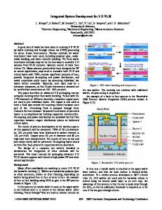
between tiers makes designing 3-D synchronous circuits even more challenging. Circuit designers may resort to designing more conservatively, or employing multiple clock domains to isolate the impact of variation. Self-timed or asynchronous circuits can tolerate drastic variations, and may help pioneer large-scale, 3-D integrated designs even if the process has not been well-characterized [16]. We designed a 3-D test chip to study the impact of process variations in 3-D integration on performance mismatch between different locations on the same tier, across different tiers, and across different assembled chips. We measure how performance of various circuits respond to temperature, and profile how heat dissipates laterally within a tier and vertically through tiers. We also demonstrate how strategic placement of heat pipes (through-vias) improves local thermal conductivity (and hence, performance) at crucial locations within the chip. Although our experiments are based on one particular process, we believe that the qualitative observations we make are relevant for similar technologies. II. E XPERIMENTAL S ETUP Process. The MIT-LL 3-D through-via process [15] was used for our design. This process offers three die stacks (tiers) and three metal layers per tier. MIT-LL 3-D features 180nm devices on a fully depleted silicon-on-insulator (FDSOI) technology, with 1.5µm tungsten-filled through-vias. During the fabrication, three 150-mm FDSOI wafers are integrated. Wafers are labeled as tiers A, B and C; with tier A being the base wafer. Handle substrates of tiers B and C are removed. Tier B is inverted, aligned and bonded to tier A using a low-temperature wafer-wafer oxide. 3-D vias are etched through the oxides, filled with tungsten and planarized using chemical-mechanical polishing. Tier C is deposited onto the structure using a similar process. During post-fabrication, bond pads and heat sink cuts are created. Circuits. Our test structures were placed on all three-tiers of the process. All of the tiers have identical circuitry for comparison purposes. Each tier was divided into a 3x3 array of identical tiles (sites), and labeled as shown in Fig. 1(a). In order to demonstrate performance degradation due to heating and to illustrate process variations of the 3-D design, we have chosen to use asynchronous (self-timed) circuits. Asynchronous circuits operate without a clock and use handshakes to communicate data. Asynchronous circuits have the capability of operating correctly at maximum local throughput
To appear, CICC 2008. Do not distribute.
(a) Fig. 1.
(b) (a) Floorplan; (b) Multiplier/divider chain
Fig. 3.
External Cooling/Heating
III. R ESULTS AND D ISCUSSION
Fig. 2. Layout of Tier C, sites s[0][2], s[1][2] and s[2][2] contain extra heat pipes; Die size is 3.2mm x 3.2mm, site size is 1mm2 approximately
in presence of continuous changes in delays through the digital logic. As opposed to synchronous designs, asynchronous circuits allow us to directly measure the maximum local throughput of each part of the circuit without making any modifications to them. Sources of delay differences include temperature, supply voltage, and process variations. Each test site consists of a valid data (token) generator connected to several frequency multipliers to attain a reasonable internal frequency. The output of the last multiplier is connected to frequency dividers, as shown in Fig. 1(b). Dividers are used to reduce the switching rate of output signals. The output of the last divider indirectly measures the frequency of the multiplier-divider junction. We can calculate the maximum throughput by monitoring the output of the last divider and multiplying by a value based on the number of the divider stages. Even though the multiplier-divider circuit occupies some area, the junction point is most sensitive to temperature variation, since that signal switches much more often than the rest of the multiplier-divider signals. The highfrequency junction is site-centered for uniform heating. At each site, a large number of wide nFET transistors surrounds the digital circuitry. These structures can act as local heat generators. Gate terminals of these heating transistors are controlled using Vthermal bias signal. Drain terminals are connected to Vthermal vdd signal. Both, Vthermal bias and Vthermal vdd , are exposed to the pins and are controlled externally. Sources of all heating transistors are tied to ground. Global signals are connected as a 3-D mesh using inter-tier vias. Sites s[0][2], s[1][2] and s[2][2] are provided with extra inter-tier vias (heat dissipation pipes) as shown in Fig. 1(a) and 2. These additional heat pipes create a temperature gradient when the circuit is generating large amount of heat.
Calibration. Prior to testing the presented structure using onchip heating transistors, the circuits were calibrated. To have a better approximation of the behavior-governing curve, we calibrated the circuit on a wide range of temperatures. The lowest temperature in our experiments was -196◦ C (77K), which is the boiling temperature of liquid nitrogen. We then slowly raised the circuit temperature to room temperature, while recording throughput of each tier at different chip temperatures. Throughput measurements were taken approximately every 20◦ C. After reaching room temperature, we placed the chip into an oven and continued taking temperature measurements and corresponding throughputs until all of the tiers on the chip stopped operating, which happened at approximately 150◦ C, as shown in Fig. 3. Before recording each data point, the chip was left in the cryogenic chamber or the oven for some time to achieve uniform temperature. Fig. 3 demonstrates that tiers A and C behave almost identically, however, the throughput of tier B is lower on the entire range of temperatures. This emphasizes the wafer-towafer process variations, since all tiers were manufactured on different wafers. All three tiers have an almost linear throughput to temperature dependence. However, for higher accuracy, we have used polynomial approximations of these curves, while performing local heating experiments as described in the next subsection. As seen in Fig. 3, circuits on tiers A and B operate correctly up to 150◦ C, however, tier C structures stop working when temperature reaches approximately 85◦ C. To demonstrate the correct operation of self-timed circuits in the presence of voltage supply variations, we performed voltage sweeps (all tiers) of the chip at -196◦ C (77K) and at room temperature, as shown in Fig. 4.
Fig. 4. V-Supply Sweeps at -196◦ C (77K) and at 21◦ C (294K) respectively
These two graphs confirm the previous observation that the throughput of tier B is less than the throughputs of the
To appear, CICC 2008. Do not distribute.
other two tiers throughout the range of tested supply voltages. The performance values of tiers A and C are almost identical during the voltage supply sweeps. Process Variation. The standard deviation of the cycle time as a percentage of the mean for a single tier was found to be 2.2% (tier A), 3.5% (tier B), and 3.7% (tier C), with the overall variation within a single chip at 10.0%. The process variation for the s[1][1] site across chips was found to be 8.2% (tier A), 11.3% (tier B), and 7.6% (tier C), with the overall variation across tiers and chips at 10.9%. For our batch of chips, the tierto-tier variations were similar to the chip-to-chip variations. Local Heat Generation. We used the calibrated chip to perform local heating experiments. For this purpose, heating transistors were utilized. In the following experiments, at each heating scenario (setting), we measured throughput of the multiplier-divider structure on all sites. This corresponds to 9 measurements per tier (3x3 sites), and 27 total measurements per chip (3 tiers) for every setting. Circuit throughput measurements at the sites enable us to calculate the temperatures of each individual site on all tiers using the three calibration curves in Fig. 3. In all of the experiments, the digital part was powered by a separate constant 1.8V supply. During the experiments, the drains (Vthermal vdd ) of all heating transistors were varied simultaneously, as well as the gates (Vthermal bias ). Each measurement was taken after the throughput of all sites settled to some steady-state value. The first setting we used was with all of the heating transistors turned off (Vthermal vdd = 0V , Vthermal bias = 0V ). This is equivalent to a self-heating setting of our structures (all 27 sites contribute to self-heating), as shown in Fig. 5(a). The site layout and heat pipe locations in this figure match the floorplan of Fig. 1(a), except all tiers are plotted in one plane. For the next heating setting, Vthermal vdd was raised. As the drain voltage increased (with transistors still off, Vthermal bias = 0V ), the leakage current through heating transistors amplified severely. This setting increased the chip temperature, which decreased the throughputs of test structures on all sites, as shown in the first several columns of Fig. 6.
tings. Grey columns, labeled norm T , represent normalized site temperatures. Site temperatures were computed by taking the throughput of test structure on the site and obtaining the corresponding temperature using the curves in Fig. 3 (separate curves were used for each tier). Temperatures for all sites under all heating settings were then normalized to site s[0][0] on tier A at Vthermal vdd = 0V , Vthermal bias = 0V (which has the value of 1 after normalization) on the Kelvin temperature scale. This normalization allows us to easily observe temperature trends across all tiers at a given setting (table columns), and also as chip temperature rises due to voltage increase on Vthermal vdd and Vthermal bias (table rows). It is important to observe that cross-tier circuit throughput difference does not necessarily translate to proportional temperature difference between the two corresponding sites. The three tiers were manufactured on different wafers and initially had a substantial throughput mismatch.
Fig. 6.
(a)
(b)
Fig. 5. (a) Self - Heating: Vthermal vdd = 0V , Vthermal bias = 0V ; (b) Temperature Increase: Vthermal vdd = 1.8V , Vthermal bias = 0.9V
Fig. 6 is organized in the following manner. The leftmost column is a sequential list of sites for tiers A, B and C (corresponding to Fig. 1(a), 5(a) and 5(b)); sites with heat pipes are shaded. The rest of the white columns, labeled f (M Hz), represent throughputs of test structures on corresponding sites at various Vthermal vdd and Vthermal bias set-
Circuit Temperature Variation Using Heating Transistors
Besides varying the drain voltages of the heating transistors, we also varied the gate voltages, which allowed direct current flow from Vthermal vdd to ground. A snapshot of the chip with Vthermal vdd = 1.8V , Vthermal bias = 0.9V is presented in Fig. 5(b). The next setting that we used was Vthermal vdd = 1.8V , Vthermal bias = 1.8V . At this setting two sites on tier A stopped working correctly due to overheating. These sites are represented by ’∼’ on the table. Our last setting was Vthermal vdd = 2.0V , Vthermal bias = 2.2V ; at this setting almost all of the sites on tier A stopped working as well as some sites on tiers B and C (also represented by ’∼’). Throughput values for each site at various settings of the heating transistors are presented in Fig. 6. As expected, temperature increases as we raise Vthermal vdd and Vthermal bias . Also, temperature decreases towards the
To appear, CICC 2008. Do not distribute.
sites with more heat pipes, since they have lower effective thermal resistance to the heat sink. The test structures’ throughputs on tiers A, B, and C are quite different, since the tiers were manufactured on separate wafers. However, on tiers A and B there is a trend that shows increasing throughput from regions without heat pipes towards the regions with heat pipes (from left to right on Fig. 5(a) and 5(b)). Tier C does not follow this trend; we attribute this difference to the fact that tier C was the top-most tier and had an additional heat escape path through the package. Some of the chips that we have tested actually had the same throughput (and temperature) variation trend on tier C as on tiers A and B. The lids on those chips, however, were sealed with epoxy (unlike the tested chip) and there was no extra escape path for heat. Nonetheless, since all of those chips had some sites that were inoperable due to manufacturing and packaging issues, we do not report detailed results from those chips. As for chip-to-chip variations, we have measured the throughput and power consumption on seven chips manufactured in the same process technology. The circuit throughput measurements for site s[1][1] (center site) with heating transistors off (Vthermal vdd = 0V , Vthermal bias = 0V ) on each tier of each chip are presented in Fig. 7 and show a large variation between the chips. All earlier presented data was obtained using Chip2. The power consumption measurements for the entire digital circuitry (all 27 sites) for all seven chips with heating transistors off (Vthermal vdd = 0V , Vthermal bias = 0V ) were normalized to the mean power and are shown in Fig. 7. The power consumption was rather consistent on five of the tested chips; however on the other two chips it was more than two times larger. Since some of the sites on the tested chips were not operational, they could have had undesired behavior that led to increased power consumption. Presented measurements and results emphasize the issues of process variation and yield in this 3-D process technology.
Fig. 7. Cross Chip Throughput Variation and Cross Chip Power Variation w/ Vthermal vdd = 0V , Vthermal bias = 0V for the s[1][1] site
IV. C ONCLUSION In this paper, we examined the variations present in 3-D circuits. Thermal dissipation and process variations on-tier, between tiers and between chips were studied. Designers have to be aware of performance and reliability issues that may arise as a result of increased heat density on different tiers. We have also verified the effectiveness of inserting through-vias as heat dissipating pipes for managing the on-chip temperature. We have demonstrated that intra-chip process variations, that
are considered minor in 2-D designs at 180nm, are much more crucial in 3-D because designers have to deal not only with intra-die variations, but also with wafer-to-wafer variations. Having different tiers of the same chip running at different frequencies presents a complication in circuit design especially when 3-D is used to partition logic circuits on multiple tiers. Asynchronous circuits offer an appealing alternative to battle the substantial process mismatch between different tiers. Several chips manufactured in the described process technology had various faults due to defects. Due to lower yields of 3-D chips, fault tolerant circuits and repetitive structures could be used to increase effective yield. Designs have to be optimized not only for performance and power consumption but also for manufacturability. Acknowledgments. We would like to thank DARPA and MIT Lincoln Labs for the opportunity to fabricate this project. We would also like to thank Christopher C. LaFrieda. R EFERENCES [1] J. Cong and Y. Zhang. Thermal-driven multilevel routing for 3d ics. In Design Automation Conference, pages 121–126. ASP-DAC, 2005. [2] C. Ferri et al. Strategies for improving the parametric yield and profits of 3d ics. In ICCAD ’07, pages 220–226, Piscataway, NJ, USA, 2007. [3] D. Fang et al. A three-tier asynchronous FPGA. In International VLSI/ULSI Multilevel Interconnection Conference, 2006. [4] K. Banerjee et al. 3-D ICs: a novel chip design for improving deepsubmicrometer interconnect performance and systems-on-chip integration. In Proceedings of the IEEE, 2001. [5] L. Xue et al. Three-Dimensional Integration: Technology, Use, and Issues for Mixed-Signal Applications. In IEEE Transactions on Electron Devices, 2003. [6] R.J. Drost et al. Proximity communication. Solid-State Circuits, IEEE Journal of, 39(9):1529–1535, Sept. 2004. [7] R.M. Lea et al. A 3-d stacked chip packaging solution for miniaturized massively parallel processing. IEEE Transactions on Advanced Packaging, 22(3):424–432, Aug 1999. [8] S. Das et al. Technology, performance, and computer-aided design of three-dimensional integrated circuits. In ISPD ’04, pages 108–115, New York, NY, USA, 2004. ACM. [9] S. Das et al. Timing, Energy, and Thermal Performance of ThreeDimensional Integrated Circuits. In ACM Great Lakes symposium on VLSI, 2004. [10] T. Kgil et al. PicoServer: Using 3d stacking technology to enable a compact energy efficient chip multiprocessor. In ASPLOS, 2006. [11] T. Y. Chiang et al. Thermal Analysis of Heterogeneous 3-D ICs with Various Integration Scenarios. In IEEE Int. Electron Devices Meeting, 2001. [12] V. Suntharalingam et al. Megapixel CMOS image sensor fabricated in three-dimensional integrated circuit technology. In IEEE Solid-State Circuits Conference, volume 1, pages 356–357, 2005. [13] W. R. Davis et al. Demistifying 3D ICs: The Pros and Cons of Going Vertical. In IEEE Design and Test of Computers, 2005. [14] B. Goplen and S. Sapatnekar. Thermal via placement in 3d ics. In ISPD ’05, pages 167–174, New York, NY, USA, 2005. ACM. [15] MIT Lincoln Labs. MITLL Low-Power FDSOI CMOS Process: Designer Guide. MIT, Cambridge,MA, 2006. [16] A. J. Martin. The limitations to delay-insensitivity in asynchronous circuits. In ARVLSI, pages 263–278. MIT, 1990. [17] K. Puttaswamy and G. H. Loh. Thermal Analysis of a 3D Die-Stacked High-Performance Microprocessor. In Great Lakes Symp. on VLSI, 2006. [18] A. Rahman and R. Reif. System-Level Performance Evaluation of Three-Dimensional Integrated Circuits. In IEEE Transactioons on VLSI Systems, 2000. [19] A. Rahman and R. Reif. Thermal Analysis of Three-Dimensional (3-D) Integrated Circuits (ICs). In IEEE Int’l Interconnect Technology Conf., IEEE Press, 2001.