Dynamically Reconfigurable SIR Filter Using Rectenna and Active Booster Abdul Quddious, Muhammad Ali Babar Abbasi, Aqeela Saghir, Salman Arain, Marco A. Antoniades, Alexis Polycarpou, Photos Vryonides and Symeon Nikolaou Published in: IEEE Transactions on Microwave Theory and Techniques Document Version: Peer reviewed version Digital Object Identifier DOI: 10.1109/TMTT.2019.2891524 Citation for published version (APA): A. Quddious et al., "Dynamically Reconfigurable SIR Filter Using Rectenna and Active Booster," in IEEE Transactions on Microwave Theory and Techniques. doi: 10.1109/TMTT.2019.2891524 Publisher rights: © 2018 IEEE. This work is made available online in accordance with the publisher’s policies. Please refer to any applicable terms of use of the publisher. General rights The authors and/or other copyright owners retain copyright and moral rights for the publications made accessible in the public portal and it is a condition of accessing publications that users recognize and abide by the legal requirements associated with these rights. • Personal use of this material is permitted. Permission from the copyright owner of the published version of this document must be obtained (e.g., IEEE) for all other uses, in current or future media, including distribution of the material or use for any profit-making activity or for advertising/promotional purposes, creating new collective works, or reuse of any copyrighted component of this work in other works. • You may freely distribute the URL/DOI identifying the publication in the public portal. Policy to take down free access If you believe that this document breaches copyright please contact us at
[email protected] providing details, and we will remove access to the work immediately and investigate your claim.
> REPLACE THIS LINE WITH YOUR PAPER IDENTIFICATION NUMBER (DOUBLE-CLICK HERE TO EDIT)
-13 dBm) is received by the RF triggered PMU’s antenna.
DC-to-DC Power Booster
PDC
PRx
PIN Diodes
Frequency Reconfigurable filter
PDC
(a)
(b)
Index Terms— Microwave filter, reconfigurable, rectenna wireless power transfer.
I.
INTRODUCTION
T
HERE has been an increasing demand for switchable and reconfigurable microwave devices, such as filters for wireless communication systems, where several different wireless devices co-exist and share the same frequency spectrum. Band pass filters (BPFs) with multi-frequency response and high stopband rejection are widely used, therefore reconfigurable BPFs can be utilized for controlling either standalone signals or combinations of information signals, with different frequency spectrum characteristics [1], [2]. In [1] a This work was supported in part by the European Union through the Erasmus Mundus INTACT Doctorate Level Mobility program. A. Quddious, A. Saghir, S. Arain, A.Polycarpou are with the Department of Electrical Engineering, Frederick University, 7, Y. Frederickou Str. Pallouriotisa, Nicosia 1036 Cyprus (e-mail:
[email protected]). M. Ali Babar Abbasi is with The Centre for Wireless Innovation (CWI), The Institute of Electronics, Communications and Information Technology (ECIT), School of Electronics, Electrical Engineering and Computer Science (EEECS), Queen's University Belfast, Belfast BT3 9DT, United Kingdom (email:
[email protected]). M.A Antoniades is with the Electrical and Computer Engineering Department, University of Cyprus, Kallipoleos 75, Nicosia 1678, Cyprus (email:
[email protected]). P. Vryonides and S. Nikolaou are with the Frederick University, and Frederick Research Center (FRC) 7, Y. Frederickou Str. Pallouriotisa, Nicosia 1036 Cyprus (e-mail:
[email protected]).
(c)
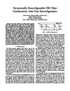
(d) Fig. 1. (a) Schematic diagram of the dynamically reconfigurable filter, (b) constituent elements of the dual-layer module (c) Layer 1-layout of the reconfigurable single-band to dual-band BPF and (d) Layer 2-RF triggered PMU (antenna + rectifier + dc-to-dc power booster).
> REPLACE THIS LINE WITH YOUR PAPER IDENTIFICATION NUMBER (DOUBLE-CLICK HERE TO EDIT)
REPLACE THIS LINE WITH YOUR PAPER IDENTIFICATION NUMBER (DOUBLE-CLICK HERE TO EDIT) < to convert the single-band SIR filter into a dual-band filter (see Fig. 1(a)). The coupled-line SIR filter operates at 2.45 GHz and in the presence of a low power (as low as -13 dBm) external RF signal at 1.6 GHz, received by an inverted-F antenna on the back side of the module, the filter behaves as a dual-band filter with an additional passband around 1.6 GHz. Both the reconfigurable filter with the full dc biasing network, and the rectenna with the cascaded dc-to-dc power booster are presented in Fig. 1(b)-(d), with the relevant geometrical dimensions shown in Table I. A. Single-Band BPF The initial layout configuration of the proposed reconfigurable BPF is shown in Fig. 2(a). It consists of four pairs of coupled-line sections and four connecting stepped impedance transmission lines. The one end of each coupled-line section is left open-ended, and the other end is connected to the transmission line with characteristic impedance Z2. The corresponding electrical lengths and characteristic impedances of the elements used, are referred to as, θ1, θ2, Ze, Zo, and Z2, as depicted in Fig. 2(a). Ze, and Zo, are the even- and odd- mode impedances of the coupled-line sections, and Z2 is the characteristic impedance of the microstrip line with width wf1 (see Fig. 1(c)). The proposed structure is symmetrical along both the vertical and horizontal axes so even- and odd-mode analysis is used to analyze the resonating modes. The even- and odd-mode equivalent circuits are shown in Fig 2(b)-(e) and the corresponding input impedance expressions are presented in (1)-(4) below. Under even-even mode excitation, the circuit is bisected firstly along the vertical axis and subsequently along the horizontal axis and the ends are terminated with an open circuit, resulting in the equivalent circuit of Fig. 2(b), and an input impedance given by: Z Z tan1tan 2 ( Z 22 Z e2 ) Z e Z 2tan 21 (1) Z in ,ee jZ e e 2 2 Z 2 Z e tan1 Z e2 tan 2 Z 22 tan 21tan 2 Under odd-odd mode excitation, the equivalent circuit in Fig. 2(c) uses Zo in both ends, however, it is terminated with an open circuit as well (instead of a short circuit) because of the physical constraint of the open-ended coupled-lines. The equivalent impedance is given by: Z Z tan1tan 2 ( Z 22 Z o2 ) Z o Z 2 tan 21 (2) Z in , oo jZ o o 2 2Z 2 Z o tan1 Z o2 tan 2 Z 22 tan 21tan 2 Similarly, the even-odd, and odd-even input impedances can be expressed as: Z o Z 2 tan1tan 2 ( Z 22 Z e Z o ) Z e Z 2tan 21 (3) Z in ,eo jZ e ( Z e Z 2 Z o Z 2 )tan1 Z e Z o tan 2 Z 22tan 21tan 2 Z in ,oe jZ o
Z e Z 2 tan1tan 2 ( Z 22 Z e Z o ) Z o Z 2tan 21 ( Z e Z 2 Z o Z 2 )tan1 Z e Z otan 2 Z 22tan 21tan 2
(4)
The resonating modes of the structure can be calculated, by setting the denominator of each equivalent impedance, equal to zero. Evidently, Zin,eo and Zin,oe have identical denominators and thus the two modes feo and foe coincide. Consequently, three distinct resonating modes, fee, foo and feo=foe exist within the passband, having the relation foo REPLACE THIS LINE WITH YOUR PAPER IDENTIFICATION NUMBER (DOUBLE-CLICK HERE TO EDIT)
REPLACE THIS LINE WITH YOUR PAPER IDENTIFICATION NUMBER (DOUBLE-CLICK HERE TO EDIT) < efficiency using a compact (44.7×33.9 mm2) substrate area. The ground shortening [31] of the PIFA antenna section allowed the antenna to be electrically small, hence a resonance frequency of 1.6 GHz was achieved with an electrically small radiator (~0.15λ). The feeding point of the antenna was selected keeping in mind that it needs to be connected directly to the rectifier. To test the stand-alone antenna, a 50 Ω transmission line was designed and it was extended to the one end of the substrate board, where an SMA connector was mounted for the Sparameter measurements of the antenna in order to verify its reliable performance before it was used as a part of the system. Fig. 8 shows the picture of the fabricated PIFA along with the simulated and measured |S11|, where the agreement between the simulation and measurement can be observed. The |S11| < -10 dB bandwidth of the antenna, lies within the range of 1.55-1.64 GHz. IV.
Fig. 9. Simulated rectifier efficiency (curve fitting) versus output load for multiple power input levels at 1.6 GHz.
RECTIFIER
The design of the rectifier had to accommodate a number of restrictions originating from the preceding PIFA, the nonconstant input impedance of the subsequent dc-to-dc power booster and the limited available space. A voltage doubler topology was preferred in an attempt to maintain low cost and a compact size at the expense of efficiency [33]. The desired characteristics of the rectifier included the highest possible RFto-dc efficiency for a wide range of RF input power levels (–25 dBm to 0 dBm), good matching at the same input power range and compact design. The RF-to-dc efficiency which has a nonlinear dependence on the termination load, was optimized for a fixed load of RL = 5.1 KΩ derived from the data sheet of the subsequent dc-to-dc power booster. The rectifier was designed at 1.6 GHz keeping in mind the lower passband of the dual-band reconfigurable filter. Keysight –ADS was used to design the microstrip traces of the rectifier. S-parameter models were imported into the ADS library in order to accurately model the required lumped components and their associated parasitics. The same RO4003C substrate that was used for the filter in Section II and for the antenna in Section III was used. Large scale signal analysis in ADS and harmonic balance simulations were used. A linear power sweep was applied from -50 dBm to 0 dBm considering the possible range of power levels of the RF scavenged signal. The rectifier should be well matched with the 50 Ω input impedance of the receiver antenna according to (9), and at the same time, it should perform with a high RF-to-dc efficiency at the available power range, according to (10), for a varying load RL. Z 50 in (9) Zin 50
Vdc2
Pout RL (10) Pin Pin Here, Zin is the impedance at the input terminal of the rectifier, Pin and Pout are the input and output power levels respectively, and Vdc is the voltage across the load resistance RL which is the input impedance of the cascaded power booster, which in turn
6
Fig. 10. Measured reflection coefficient of the rectifier at different power levels. The standalone fabricated prototype of the rectifier is shown in the inset.
depends on the biasing conditions. The efficiency of the rectifier is non-linearly dependent on the termination load, the resistance RL. On the other hand, as it will be elaborated in the subsequent Section V, the impedance of the power booster is dependent on both the enabling voltage VEN and the VCC biasing voltage. Before cascading the rectifier with the power booster, the effect on the rectifier efficiency when RL changed has to be investigated. An analysis was carried out, in which RL was varied from 100 Ω to 1 MΩ. Fig. 9 shows the plots of the simulated efficiency for multiple input power levels vs load RL. A logarithmic scale is used for the RL values. Fig. 9 indicates that within the range from 4205 - 6700 Ω which is the actual range for the measured RL values on the dc-to-dc active power booster, the rectifier operates close to its maximum efficiency region for various input power levels. For the rectifier design, initially, a standard voltage doubler was designed along a 50 Ω microstrip line at 1.6 GHz. Two problems were encountered: a) the bandwidth of the rectifier was very narrow and as a result good matching within the entire input power range could not be maintained, and b) as a result of the relatively low operation frequency of the rectifier, the physical size of the rectifier features (especially lt, ls1 and ls2) was too large to fit in the available space. To overcome the first problem, a radial stub was introduced instead of linear open stub. As shown in Fig. 1(d), the rectifier circuit begins from the end of the receiver antenna, and a curved transmission line section hosts the shorted stub and a radial stub
> REPLACE THIS LINE WITH YOUR PAPER IDENTIFICATION NUMBER (DOUBLE-CLICK HERE TO EDIT) < placed at the point where sufficient area was available. This rectifier shape and dimensions were dictated based on the results of a multivariable optimization in ADS. A quasi-Newton algorithm was used with two output goals: a) |S11| < -15 dB at 1.6 GHz, and b) maximum possible RF-to-dc efficiency. Subsequently and for the given rectifier traces, capacitances C01 and C02 were re-optimized considering the available lumped component values from the Murata component library [34]. In addition to this, during every optimization step, the |S11| of the rectifier at discrete input power levels (-25 to -10 dBm) was carefully observed to ensure acceptable matching within the targeted power range. The final values of the capacitors used, were: C01 = 139 pF and C02 = 150 pF. The photograph of the rectifier is presented in the inset of Fig. 10 and the fabricated set of feature values is summarized in Table I. The rectifier was designed and tested separately as a stand-alone device before using as part of the entire RF triggered PMU. Fig. 10 shows that the |S11| is below -10 dB from 1.57 to 1.61 GHz, giving a measured bandwidth of 40 MHz. The measured efficiency of the rectifier was calculated by measuring the dc voltage across RL while changing the input power level Pin from a signal generator (Rohde & Schwarz SMF100A) at 1.6 GHz. The waveform used in this experiment was an unmodulated sine wave. The power level was varied from -25 dBm to 0 dBm with a step size of 2.5 dBm. The simulated and measured output voltage across RL = 5.1 KΩ is shown in Fig. 11. Equation (10) was used to calculate the measured efficiency of the rectifier, presented in Fig. 11 vs the Pin. It is important to point out that the efficiency of the rectifier depends not only on the performance of voltage doubler circuit, but also on the quality of impedance matching at the input terminal of the rectifier. The final parameters presented in Table I ensure an optimized matching condition as well as maximum achievable efficiency of the rectifier at a given Pin. The design strategy for the matching network takes into consideration both the timedependent nature of the power booster’s switching operation, and the time-varying RF actuation signal received by the PIFA. To describe this, let us look at the rectifier performance at a static Pin condition. Fig. 12(a) shows the dependence of Vrect, and Irect on the optimal Prect at the varying load RL at Pin = 31.6 μW (-15 dBm). The operation of the device resides where V and I combination is ~0.31V and ~60 µA respectively, which is very close to the ideal power condition of any Vrect, Irect combination. Fig. 12(b) shows the simulated efficiency as a two-variable function, depending at any time from Pin and RL non-linearly. An in-depth discussion on this is presented in Section VI. The measured and simulated results are in good agreement. From Fig. 12, it can be seen that the efficiency of the rectifier increases from 20% to 49% when the input power level increases from -25 dBm to -10 dBm. For the critical -13 dBm input power required for the p-i-n diode biasing, the
7
Fig. 11. Simulated and measured rectifier output voltage and the efficiency across the 5.1 KΩ load at 1.6 GHz versus the input power.
(a)
(b)
Fig. 12 (a) Load current consumption versus Vrect and Prect at Pin = -15 dBm (b) Rectifier efficiency for combined Pin and RL variations. Both results are based on simulations. TABLE II RF-TO-DC CONVERSION EFFICIENCY VERSUS FREQUENCY AND INPUT POWER Ref. This work [12] [13] [14] [15] [16] [18] [24] [25] [35] [36]
Freq. (GHz) 1.60 0.85 0.85 1.85 2.45 0.47 – 0.77 2.45 0.90, 1.75 0.90 0.86 2.45
Pin (dBm) -25, -10 -20, -10 -20, -10 -20 -20 -40, -20 25 -8.77, -16.27 -10 -25, -10 -17.2
Efficiency 16.5%, 49.0% 20%, 37% 20.5%, 35.3% 15.0% 15.0% 0.4%, 18.2% 65.0% 44.5%, 34.5% 33.0% 17%, 44.0% 50.0%
efficiency is 47% and the output voltage 0.43 V. The rectifier has been tested using a single tone signal at 1.6 GHz to ensure fair comparison with the referenced rectifier designs summarized in Table II. It can be observed that the proposed rectifier compares favorably with other recently reported designs. V.
DC-TO-DC POWER BOOSTER
The proposed dynamically reconfigurable dual-band filter requires four p-i-n diodes to achieve the desired reconfigurability. To actuate a single p-i-n diode (Skyworks SMP1345), a minimum power of 9 mW is required, since around a 0.89 V voltage and 10 mA current are needed for each diode. The four p-i-n diodes are simultaneously set in the “ON” state, therefore a total of 36 mW (15.6 dBm) of dc power is required. For realistic wirelessly received RF power levels, the amount of harvested dc power from the rectifier output is not sufficient to directly actuate the p-i-n diodes, therefore an active
> REPLACE THIS LINE WITH YOUR PAPER IDENTIFICATION NUMBER (DOUBLE-CLICK HERE TO EDIT) < C1F 1μF
C2F 1μF
7 2 4 8 2 x IN INPUT C1- C1+ C2- C2+ 5 OUTPUT Max 40 mA 0.9 V to 1.8 V 3 OUT1 + VCC C(OUT1) VCC + CIN + 1μF 1μF Not TPS60301 6 OUT2 Connected + C(OUT2) 1 1μF 10 VEN EN PG GND OFF/ON 9
Fig. 13. Schematic of the dc-to-dc active power booster designed using the charge pump IC model: TPS60301.
dc-to-dc power booster is introduced. The device is able to convert dc voltage from a lower level to a higher level, when an enabling voltage signal is above a threshold. A charge pump Integrated Circuit (IC) model: TPS60301 [37] with dual output, from Texas Instruments is used, as is shown in Fig. 13. The charge pump requires a dc voltage supply, VCC between 0.9 V and 1.8 V. It has a logic controlled input (enabling input VEN) and delivers an output (VOUT1) dc voltage approximately two times the VCC voltage. Only one of the two available output terminals of the IC is used, while the second terminal remains unconnected. Along with this IC, five 1 µF capacitors are used. The capacitors are required to build a complete high efficiency charge pump dc-to-dc power booster (sometimes also referred to as a boost converter) as can be seen in the schematic of Fig. 13. In this schematic, C1F and C2F are used as flying capacitors, while, C(OUT1), C(OUT2) and CIN are used as filter capacitors that bypass any pulse or noise to the ground. For every combination of the varying operating conditions of the active dc-to-dc power booster, (i.e. VCC ranging from 0.9-1.8 V and VEN ranging from 0.0-1.5 V), the measured input impedance (RL termination load for the preceding rectifier) of the dc-to-dc power booster, as measured between the EN and GND terminals, remains between 4205 Ω and 6700 Ω. When VEN is “high” and OUT2 (terminal 6) is not connected, OUT1 (terminal 5) can deliver a maximum of 40 mA and approximately two times the VCC voltage. The device is enabled when VEN is set from logic “low” (< 0.5×VCC) to logic “high” (>0.5×VCC). Considering that the minimum required VCC is 0.9V, this means that a minimum of 0.45V is needed from the output of the rectifier in order to make the power at the terminal OUT1 available to the p-i-n diodes. Measurements presented in Section VII indicated that this minimum enabling voltage was actually 0.43 V. From Fig. 11, the required received RF power from the rectifier has to be higher than -13 dBm. For the rectifier’s converted voltage calculation, the power booster’s input impedance was approximated to be 5.1 KΩ. Experimentally, with the input RF power controlled from a signal generator (R&S SMF100A) directly feeding the rectifier, the diodes were successfully forward biased with as low as -13 dBm RF power. The power booster first enters a dc start-up mode during which the flying capacitor COUT1 will charge up to ~VCC. After that, the charge pump IC starts switching to boost the voltage further up to about two times VCC. When VEN goes
8
back to logic “low”, it disables all internal circuits, and consequently it reduces the output current to only 0.05 µA. The device exits the “shutdown state” once VEN is set to logic “high” again. The typical no-load, start-up time of the power booster is 400 µs. VI.
RF TRIGGERED PMU COMBINED MODULE
The inverted-F antenna from Section III is connected to the rectifier from Section IV forming a rectenna, and subsequently the rectenna is connected to the active dc-to-dc power booster that operates as a power management unit. The related theoretical analysis is thoroughly addressed in [38]-[39] and references therein. The theoretical principals of PIFA design can be found in the classical literature [40]-[41]. The combined module can be considered an RF triggered PMU since the rectified input RF signal is used to enable the delivery of the dc power to the four p-i-n diodes used for the dynamic reconfiguration of the SIR single-band/dual-band BPF presented in Section II. The power for the forward biasing of the four p-i-n diode switches is provided from the active power booster. In the previous sections, the antenna, the rectifier and the dc-to-dc power booster were discussed independently as stand-alone devices. This section discusses the combined RF triggered PMU system presented in Fig. 1(d) where the constituent components are combined into a single module. In [35] it was shown that, the variation of the input power level may affect the matching, and the -10 dB bandwidth may actually shift away from the design frequency. Therefore, it is important to ensure good impedance matching between the antenna and the rectifier for multiple power levels. The optimization conditions mentioned in Section IV and the consequent geometrical parameters met this condition. In Fig. 10, the measured |S11| plots of the rectifier are compared when the input power levels vary from -25 to -10 dBm. The rectifier operational bandwidth (|S11| < -10dB) is observed to be within 1.576 –1.628 GHz, 1.558 – 1.618 GHz and 1.550 – 1.611 GHz for input power levels of -5, -15 and -25 dBm, respectively, ensuring that the rectenna is well matched for all the related power levels. Moreover, the measured RL values (4205 - 6700 Ω) which correspond to the input impedance of the dc-to-dc power booster under the required biasing conditions are fairly close to the impedances for which the maxima of the efficiency plots are observed (Fig. 9). Consequently the implemented combined module ensures the successful operation for a broad and practically time varying range of input power levels, and for considerably varying RL values, despite the rectifier’s non-linear dependence on both Pin and RL parameters, as defined in (10). The practically available 1.6 GHz signals include both LongTerm Evolution (LTE) B24 signals and commercial Global Positioning System (GPS) signals. Any received 1.6 GHz signal is processed in baseband using a Digital Signal processor (DSP) processor. If the received signal is classified as undesired a digital “flag” control signal will be generated, “0”, and will be directed through an AND gate in the EN pin of the TPS60301 circuit. This way if the DSP controller does not classify the
> REPLACE THIS LINE WITH YOUR PAPER IDENTIFICATION NUMBER (DOUBLE-CLICK HERE TO EDIT) < signal as desired the filter will not allow the second passband. However if the signal is classified as desired the combination of the generated “1” in the AND gate will allow the passband at 1.6 GHz. Note that the power level of LTE B24 signals and GPS signals differ by orders of magnitude. While the GPS signal level is around -120 dBm (below the minimum power that can be detected or rectified by the rectifier), LTE B24 [42] (1600 L-band having 1626.5 – 1660.5 MHz uplink and 1525 – 1559 MHz downlink) with a Base Station (BS) EIRP of +31.9dBW/200KHz is practically adequate (assuming ideal free space propagation conditions) for triggering the power booster several meters away from the transmitter. Although the presented work is a proof of concept of a novel approach for dynamically reconfigurable passives, the filter was designed for the LTE B24/GPS (1.6 GHz) bands and the Wi-Fi (2.4 GHz) band and it could be exploited by any everyday device (tablet, cellphone) that uses both these applications.
(a)
9
(b)
Fig. 14. Fabricated prototype of the DUT (a) Top view showing the dynamically reconfigurable SIR BPF filter, and (b) rear view showing the RF triggered PMU.
Signal Generator
Tx Antenna
d
Rx Antenna
Spectrum Analyzer
(a)
VII.
IMPLEMENTATION AND TESTING
Photographs of the fabricated prototype of the proposed dynamically reconfigurable SIR filter are presented in Fig. 14. Fig. 14(a) shows the top view of the module where the filter is realized, and Fig. 14(b) shows the rear view where the RF triggered PMU module is built. For the fabrication, two Rogers RO4003C boards were used which were placed back to back having a common RF ground. On the first board the filter was fabricated and the p-i-n diodes and the RF choke inductors were soldered (Fig 14(a)). On the second board, the antenna, the rectifier’s microstrip traces and the dc circuit footprint for the charge pump IC and its peripherals were created using an LPKF ProtoMat H100 milling machine. Both the rectifier’s matching stubs and the PIFA were shorted to the common RF ground using vias through 0.4 mm diameter holes. The exact physical locations of the vias are presented as red dots in Fig. 1(d). Then, on both sides of the module the required lumped components were soldered. P-i-n diodes (Skyworks DSM8100-000 [43]), and RF choke inductors (Coilcraft series 0402CS-82 nH [44]) were used for the reconfigurable filter. Schottky diodes (Skyworks SMS7630-079LF [45]) and capacitors (Murata series GJM03-139 pF and 150 pF [34]) were used for the rectifier and finally a charge pump IC (Texas Instruments TPS60301) with five capacitors (Murata series GJM03-1 µF [34]) was used for the power booster implementation. The dc circuit associated to the RF triggered PMU module is shown Fig. 1(d). Metallic pads indicated in the annotations used for wire soldering corresponds to the IC pin configuration and PCB layout [37]. SMA connectors were attached in order to measure the filter’s S-parameters. Insulated wires were used to connect the OUT1 terminal of the IC to the biasing pads on the filter board side. Finally, the two boards were attached back-to-back so that the RF ground layers of both boards coincided with each other. Low loss glue was used to ensure adhesiveness between the two joint boards in order to realize a single module of the dual-layer dynamically reconfigurable single- to dual-band SIR filter with an integrated RF triggered PMU. The measurement setup, implemented in order to evaluate the performance of the device under test (DUT), is presented in Fig. 15. Initially, a signal generator was connected to a replica of the
Signal Generator
Tx Antenna d
DUT
VNA
(b) Fig. 15. Measurement process setup: (a) signal generator-transmitter PIFA and receiver PIFA-spectrum analyzer (b) signal generator- receiver antenna and DUT connected with VNA.
Fig. 16. Simulated and measured open-circuit voltage at the rectifier output terminal versus input power.
PIFA antenna and was used as a transmitter antenna. A second identical antenna was used as a receiver antenna and was connected to a spectrum analyzer (Anritsu MS2668C). Note that the transmitter PIFA in this experiment was only used because of its availability. Any antenna type with a known gain can be used to repeat the same experimental setup. The received power was measured while the distance between two antennas “d” was recorded to create a set of distances with the corresponding RF Pin levels at the input of the rectifier. Next, the receiver antenna and the spectrum analyzer were removed, and replaced with the rectenna. The open circuit voltage at the output terminal of the rectifier was measured, for the same set
> REPLACE THIS LINE WITH YOUR PAPER IDENTIFICATION NUMBER (DOUBLE-CLICK HERE TO EDIT)
-13 dBm). When the received power is high enough the output of the rectifier (VRect) is higher than 0.43V and the output of the booster (VBooster) rises to 1.8V, high enough to actuate the p-i-n diodes and cause the dual-band response. When the RF signal is blocked VRect goes to zero and VBooster drops below the 0.9V which is the minimum diode actuation voltage depicted in Fig. 18. As a result the diodes remain unbiased and the filter response remains singleband. Fig 17(b) shows that when PRx power is below -13 dBm the variations in the rectifier output voltage (VRect) do not have any effect on VBooster, since they are below the minimum required 0.43 V threshold. In order to demonstrate the dynamic response of the filter according to the power level of the external interferer in a continuous, real-time manner the rectified voltage VRect and VBooster were recorded when the distance between the transmitter and the rectenna was continuously varied. The results are presented in Fig. 18. When VRect (blue line) rises above the 0.43 V threshold VBooster (red line) rises instantly to 1.8 V and biases the diodes making the filter dual-band. However, when the distance is big enough to drop the rectified voltage VRect below 0.43 V, VBooster drops below the diode actuation voltage (0.9 V) and the filter becomes single-band. In order to verify the successful implementation and the performance of the DUT, S-parameter measurements (Fig. 6 and 7) of the dual-layer filter shown in Fig. 14 were taken in
> REPLACE THIS LINE WITH YOUR PAPER IDENTIFICATION NUMBER (DOUBLE-CLICK HERE TO EDIT) < both the absence and presence of the RF triggering signal. The setup is presented in Fig. 15(b). Test resistor in Fig. 14(b) was disconnected before the final measurements. RF signals at multiple power levels were generated by the signal generator and were used to wirelessly and dynamically actuate the p-i-n diodes and reconfigure the BPF from different distances between the transmitter and the receiver antennas. The measurement results of the DUT are summarized in Table III. It can be seen that in all cases, a received power greater than approximately -13 dBm successfully actuates the p-i-n diodes, and thus achieves the desired reconfiguration of the SIR filter from a single-band to a dual-band response. It is worth mentioning that for a power level below -13 dBm, the primary design principle for the RF triggered PMU combined module will change drastically. First, the rectifier design needs to exploit the full potential of unconventional methods to realize higher DC conversation efficiency. Secondly, as mentioned before, the PMU is optimized for peak performance with the physically achievable rectifier’s efficiency presented in section IV. An alternative approach could be a fully passive PMU with ultra-low power dc-to-dc passive converter based on voltagestepping up transformer, field effect transistor (FET) and an oscillator [46]. In addition, it has to be pointed out that the variation of VRect (as long as VRect >0.43 V) does not affect the filter’s dual-band response which remains the same as the one shown in Fig 6 The only thing that effectively affects the filter response is whether VRect is higher or lower than the 0.43 V threshold.
a single- to dual-band filter has been successfully implemented and tested. The filter operates as a single-band BPF with low insertion loss (0.84 dB) and 15% fractional bandwidth, at 2.45 GHz intended for WiFi applications while in the presence of a wireless signal as low as -13 dBm it converts into a dual-band BPF. For the additional dynamically formed passband around 1.6 GHz the insertion loss is 1.2 dB and the fractional bandwidth is 12.7%. In both single- and dual-band operation states the BPF shows a wide stopband (>3×fo) at the high frequency band with high |S21| suppression ( REPLACE THIS LINE WITH YOUR PAPER IDENTIFICATION NUMBER (DOUBLE-CLICK HERE TO EDIT) < [16]
[17]
[18]
[19]
[20]
[21]
[22]
[23]
[24]
[25]
[26]
[27]
[28]
[29]
[30]
[31] [32] [33]
[34]
[35]
[36]
[37]
C. Mikeka, H. Arai, A. Georgiadis, and A. Collado, "DTV band micropower RF energy-harvesting circuit architecture and performance analysis," in 2011 IEEE International Conference on RFIDTechnologies and Applications, Sitges, 2011, pp. 561-567. M. Piñuela, P. D. Mitcheson, and S. Lucyszyn, "Ambient RF Energy Harvesting in Urban and Semi-Urban Environments," IEEE Trans. Microw. Theory Techn., vol. 61, no. 7, pp. 2715-2726, May. 2013. J. Zbitou, M. Latrach, and S. Toutain, "Hybrid rectenna and monolithic integrated zero-bias microwave rectifier," IEEE Trans. Microw. Theory Techn., vol. 54, no. 1, pp. 147-152, Jan. 2006. J. A. Hagerty, F. B. Helmbrecht, W. H. McCalpin, R. Zane, and Z. B. Popovic, "Recycling ambient microwave energy with broad-band rectenna arrays," IEEE Trans. Microw. Theory Techn., vol. 52, no. 3, pp. 1014-1024, Mar. 2004. J. A. G. Akkermans, M. C. v. Beurden, G. J. N. Doodeman, and H. J. Visser, "Analytical models for low-power rectenna design," IEEE Antennas Wireless Propag. Lett., vol. 4, pp. 187-190, Jun. 2005. E. Falkenstein, M. Roberg, and Z. Popovic, "Low-Power Wireless Power Delivery," IEEE Trans. Microw. Theory Techn., vol. 60, no. 7, pp. 2277-2286, May. 2012. P. Ji-Yong, H. Sang-Min, and T. Itoh, "A rectenna design with harmonic-rejecting circular-sector antenna," IEEE Antennas Wireless Propag. Lett., vol. 3, no. 1, pp. 52-54, Jan. 2005. A. Dolgov, R. Zane, and Z. Popovic, "Power management system for online low power RF energy harvesting optimization," IEEE Trans. Circuits Syst. I: Regular Papers, vol. 57, no. 7, pp. 1802-1811, Jan. Jan. 2010. A. Costanzo, A. Romani, D. Masotti, N. Arbizzani, and V. Rizzoli, "RF/baseband co-design of switching receivers for multiband microwave energy harvesting," Sens. Actuator A-Phys., vol. 179, pp. 158-168, Jun. 2012. D. Masotti, A. Costanzo, P. Francia, M. Filippi, and A. Romani, "A loadmodulated rectifier for RF micropower harvesting with start-up strategies," IEEE Trans. Microw. Theory Techn., vol. 62, no. 4, pp. 9941004, Apr. 2014. R. Zhang and L. Zhu, "Design of a compact dual-band bandpass filter using coupled stepped-impedance resonators," IEEE Microw. Wireless Compon. Lett., vol. 24, no. 3, pp. 155-157, Jan. 2014. Z. Zhang, Y.-C. Jiao, X.-M. Wang, and S.-F. Cao, "Design of a compact dual-band bandpass filter using opposite hook-shaped resonator," IEEE Microw. Wireless Compon. Lett., vol. 21, no. 7, pp. 359-361, Jul. 2011. R. Zhang and L. Zhu, "Synthesis and design of wideband dual-band bandpass filters with controllable in-band ripple factor and dual-band isolation," IEEE Trans. Microw. Theory Techn., vol. 61, no. 5, pp. 18201828, May. 2013. H. Zhu and A. M. Abbosh, "Single-and Dual-Band Bandpass Filters Using Coupled Stepped-Impedance Resonators With Embedded Coupled-Lines," IEEE Microw. Wireless Compon. Lett., vol. 26, no. 9, pp. 675-677, Aug. 2016. Radio-Electronics.com. (September). WiFi Channels, Frequencies Bands and Bandwidths. [online] Available: https://www.radioelectronics.com/info/wireless/wi-fi/80211-channels-numberfrequencies-bandwidth.php Accessed on: Sep. 2018. R. C. Hansen and R. E. Collin, "Electrically small antennas: canonical types" in Small antenna handbook, Wiley-IEEE Press, 2011, pp. 93-113. K.-L. Wong, "Compact broadband microstrip antennas" in Compact and broadband microstrip antennas. John Wiley & Sons, 2004, pp. 45-79. J. C. Salmon, "Circuit topologies for single-phase voltage-doubler boost rectifiers," IEEE Trans. Power Electron., vol. 8, no. 4, pp. 521-529, Oct. 1993. M. E. N. America. (2017). Ceramic Capacitor Kit [online] Available: https://www.digikey.co.uk/product-detail/en/murata-electronics-northamerica/GJM03-KIT-TTOL-DE/490-12155-ND/5414396, Accessed on: Feb. 2016. S. D. Assimonis, S. N. Daskalakis, and A. Bletsas, "Sensitive and Efficient RF Harvesting Supply for Batteryless Backscatter Sensor Networks," IEEE Trans. Microw. Theory Techn., vol. 64, no. 4, pp. 1327-1338, Mar. 2016. H. Sun, Y. x. Guo, M. He, and Z. Zhong, "Design of a High-Efficiency 2.45-GHz Rectenna for Low-Input-Power Energy Harvesting," IEEE Antennas Wireless Propag. Lett., vol. 11, pp. 929-932, Aug. 2012. T. Instruments. (February). Texas Instruments Charge Pump IC: TPS60301. [online] Available: http://www.ti.com/product/TPS60301, Accessed on: Feb. 2016.
[38]
[39]
[40]
[41]
[42]
[43]
[44]
[45]
[46]
12
A. Boaventura, A. Collado, N. B. Carvalho and A. Georgiadis, "Optimum behavior: Wireless power transmission system design through behavioral models and efficient synthesis techniques," IEEE Microw. Mag., vol. 14, no. 2, pp. 26-35, Mar. 2013. A. Costanzo, M. Fabiani, A. Romani, D. Masotti and V. Rizzoli, "Codesign of ultra-low power RF/Microwave receivers and converters for RFID and energy harvesting applications," in Proc. IEEE MTT-S IMS, Anaheim, CA, May 2010, pp. 856-859. B. Kevin, "Radiating and balanced mode analysis of PIFA shorting pins," in Proc. IEEE ISAP, San Antonio, TX, USA, vol.4, Jun. 2002, pp. 508-511. T. Taga and K. Tsunekawa, "Performance Analysis of a Built-In Planar Inverted-F Antenna for 800 MHz Band Portable Radio Units," IEEE J. Sel. Areas Commun., vol. 5, no. 5, pp. 921-929, Jun. 1987. F. C. Commission. (September). FCC Rules ATC 25.253. [online] Available: https://www.gpo.gov/fdsys/pkg/CFR-2010-title47vol2/pdf/CFR-2010-title47-vol2-sec25-253.pdf Accessed on: Sep. 2018. S. Solutions. (February). PIN Diodes Available: http://www.skyworksinc.com/Product/251/DSM8100-000 Accessed on: Feb. 2016. Coilcraft. (February). Fixed Inductors 0402CS [online]. Available: https://eu.mouser.com/datasheet/2/597/0402cs-253326.pdf, Accessed on: Feb. 2016. S. Solutions. (February). Schottkey diode [online]. Available: http://www.skyworksinc.com/Product/511/SMS7630_Series, Accessed on: Feb. 2016. S. Adami, V. Marian, N. Degrenne, C. Vollaire, B. Allard and F. Costa, "Self-powered ultra-low power DC-DC converter for RF energy harvesting," in Proc. IEEE Faible Tension Faible Consommation, Paris, pp. 1-4, Jun. 2012.